 | –≠–ª–µ–∫—Ç—Ä–æ–Ω–Ω—ã–π –∫–æ–º–ø–æ–Ω–µ–Ω—Ç: FDS8936A | –°–∫–∞—á–∞—Ç—å:  PDF PDF  ZIP ZIP |
May 1998
FDS8936A
Dual N-Channel Enhancement Mode Field Effect Transistor
General Description Features
Absolute Maximum Ratings
T
A
= 25
o
C unless otherwise noted
Symbol
Parameter
FDS8936A
Units
V
DSS
Drain-Source Voltage
30
V
V
GSS
Gate-Source Voltage
±20
V
I
D
Drain Current - Continuous
(Note 1a)
6
A
- Pulsed
20
P
D
Power Dissipation for Dual Operation
2
W
Power Dissipation for Single Operation
(Note 1a)
1.6
(Note 1b)
1
(Note 1c)
0.9
T
J
,T
STG
Operating and Storage Temperature Range
-55 to 150
∞C
THERMAL CHARACTERISTICS
R
JA
Thermal Resistance, Junction-to-Ambient
(Note 1a)
78
∞C/W
R
JC
Thermal Resistance, Junction-to-Case
(Note 1)
40
∞C/W
FDS8936A Rev.B
6 A, 30 V. R
DS(ON)
= 0.028
@ V
GS
= 10 V,
R
DS(ON)
= 0.040
@ V
GS
= 4.5 V.
High density cell design for extremely low R
DS(ON)
.
High power and current handling capability in a widely
used surface mount package.
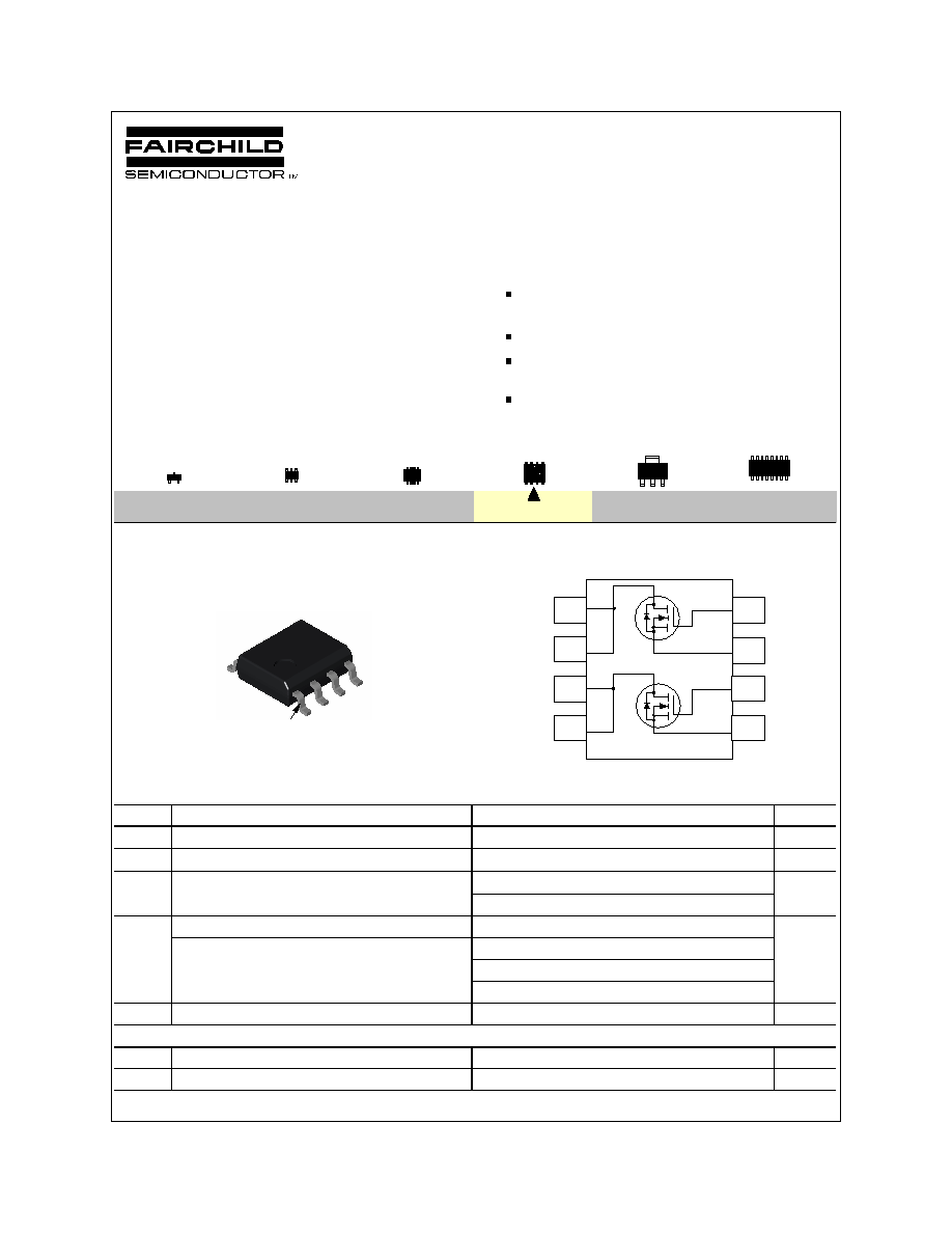
Dual MOSFET in surface mount package.
SOT-23
SuperSOT
TM
-8
SOIC-16
SO-8
SOT-223
SuperSOT
TM
-6
SO-8 N-Channel enhancement mode power field effect
transistors are produced using Fairchild's proprietary, high
cell density, DMOS technology. This very high density
process is especially tailored to minimize on-state resistance
and provide superior switching performance. These devices
are particularly suited for low voltage applications such as
notebook computer power management and other battery
powered circuits where fast switching, low in-line power loss,
and resistance to transients are needed.
1
5
7
8
2
3
4
6
S1
D1
S2
G1
SO-8
D2
D2
D1
G2
FDS
8936A
pin
1
© 1998 Fairchild Semiconductor Corporation
Electrical Characteristics (
T
A
= 25
O
C unless otherwise noted )
Symbol
Parameter
Conditions
Min
Typ
Max
Units
OFF CHARACTERISTICS
BV
DSS
Drain-Source Breakdown Voltage
V
GS
= 0 V, I
D
= 250 µA
30
V
BV
DSS
/
T
J
Breakdown Voltage Temp. Coefficient
I
D
= 250 µA, Referenced to 25
o
C
32
mV/
o
C
I
DSS
Zero Gate Voltage Drain Current
V
DS
= 24 V, V
GS
= 0 V
1
µA
T
J
= 55∞C
10
µA
I
GSSF
Gate - Body Leakage, Forward
V
GS
= 20 V, V
DS
= 0 V
100
nA
I
GSSR
Gate - Body Leakage, Reverse
V
GS
= -20 V, V
DS
= 0 V
-100
nA
ON CHARACTERISTICS
(Note 2)
V
GS(th)
Gate Threshold Voltage
V
DS
= V
GS
, I
D
= 250 µA
1
1.7
3
V
V
GS(th)
/
T
J
Gate Threshold Voltage Temp. Coefficient
I
D
= 250 µA, Referenced to 25
o
C
-4
mV/
o
C
R
DS(ON)
Static Drain-Source On-Resistance
V
GS
= 10 V, I
D
= 6 A
0.023
0.028
T
J
=125∞C
0.036
0.048
V
GS
= 4.5 V, I
D
= 4.8 A
0.034
0.004
I
D(ON)
On-State Drain Current
V
GS
= 10 V, V
DS
= 5 V
20
A
g
FS
Forward Transconductance
V
DS
= 5 V, I
D
= 6 A
19
S
DYNAMIC CH ARACTERISTICS
C
iss
Input Capacitance
V
DS
= 15 V, V
GS
= 0 V,
f = 1.0 MHz
650
pF
C
oss
Output Capacitance
345
pF
C
rss
Reverse Transfer Capacitance
95
pF
SWITCHING CHARACTERISTICS
(Note 2)
t
D(on)
Turn - On Delay Time
V
DS
= 10 V, I
D
= 1 A
8
16
ns
t
r
Turn - On Rise Time
V
GS
= 10 V , R
GEN
= 6
14
25
t
D(off)
Turn - Off Delay Time
23
37
t
f
Turn - Off Fall Time
9
18
Q
g
Total Gate Charge
V
DS
= 10 V, I
D
= 6 A,
19
27
nC
Q
gs
Gate-Source Charge
V
GS
= 10 V
3.2
Q
gd
Gate-Drain Charge
4.3
DRAIN-SOURCE DIODE CHARACTERISTICS AND MAXIMUM RATINGS
I
S
Maximum Continuous Drain-Source Diode Forward Current
1.3
A
V
SD
Drain-Source Diode Forward Voltage
V
GS
= 0 V, I
S
= 1.3 A
(Note 2)
0.7
1.2
V
Notes:
1. R
JA
is the sum of the junction-to-case and case-to-ambient thermal resistance where the case thermal reference is defined as the solder mounting surface of the drain pins. R
JC
is guaranteed by
design while R
CA
is determined by the user's board design.
Scale 1 : 1 on letter size paper
2. Pulse Test: Pulse Width < 300µs, Duty Cycle < 2.0%.
FDS8936A Rev.B
c. 135
O
C/W on a 0.003 in
2
pad of 2oz copper.
b. 125
O
C/W on a 0.02 in
2
pad of 2oz copper.
a. 78
O
C/W on a 0.5 in
2
pad of 2oz copper.
FDS8936A Rev.B
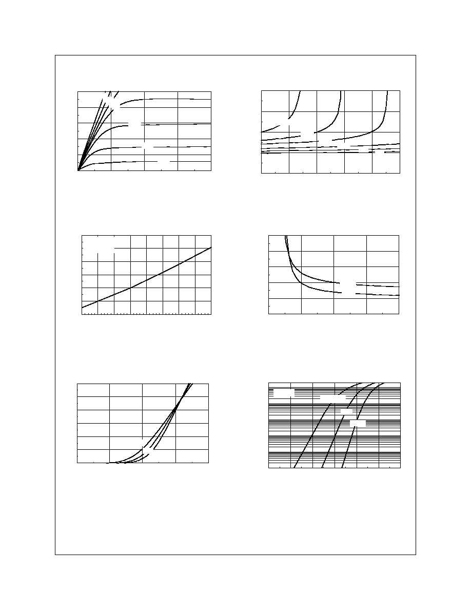
0
1
2
3
4
0
6
12
18
24
30
V , DRAIN-SOURCE VOLTAGE (V)
I , DRAIN-SOURCE CURRENT (A)
DS
D
4.0V
3.5V
V =10V
GS
4.5V
6.0V
3.0V
5.0V
0
6
12
18
24
30
0
1
2
3
4
I , DRAIN CURRENT (A)
DRAIN-SOURCE ON-RESISTANCE
D
V = 3.5V
GS
R , NORMALIZED
DS(ON)
7.0V
5.5 V
4.0 V
4.5 V
10V
Typical Electrical Characteristics
Figure 1. On-Region Characteristics.
Figure 2. On-Resistance Variation with
Drain Current and Gate Voltage.
-50
-25
0
25
50
75
100
125
150
0.6
0.8
1
1.2
1.4
1.6
1.8
T , JUNCTION TEMPERATURE (∞C)
DRAIN-SOURCE ON-RESISTANCE
J
R , NORMALIZED
DS(ON)
V = 10V
GS
I = 6A
D
Figure 3. On-Resistance Variation With
Temperature
.
1
2
3
4
5
0
5
10
15
20
25
30
V , GATE TO SOURCE VOLTAGE (V)
I , DRAIN CURRENT (A)
V = 10V
DS
GS
D
T = 125∞C
J
-55∞C
25∞C
Figure 5. Transfer Characteristics.
0
0.2
0.4
0.6
0.8
1
1.2
0.0001
0.001
0.01
0.1
1
20
V , BODY DIODE FORWARD VOLTAGE (V)
I , REVERSE DRAIN CURRENT (A)
25∞C
-55∞C
V = 0V
GS
SD
S
T = 125∞C
J
Figure 6. Body Diode Forward Voltage
Variation with Source Current
and Temperature.
2
4
6
8
10
0
0.02
0.04
0.06
0.08
0.1
V , GATE TO SOURCE VOLTAGE (V)
GS
R , ON-RESISTANCE (OHM)
DS(ON)
125∞C
25∞C
I = 3A
D
Figure 4. On-Resistance
Variation with
Gate-to-Source Voltage.
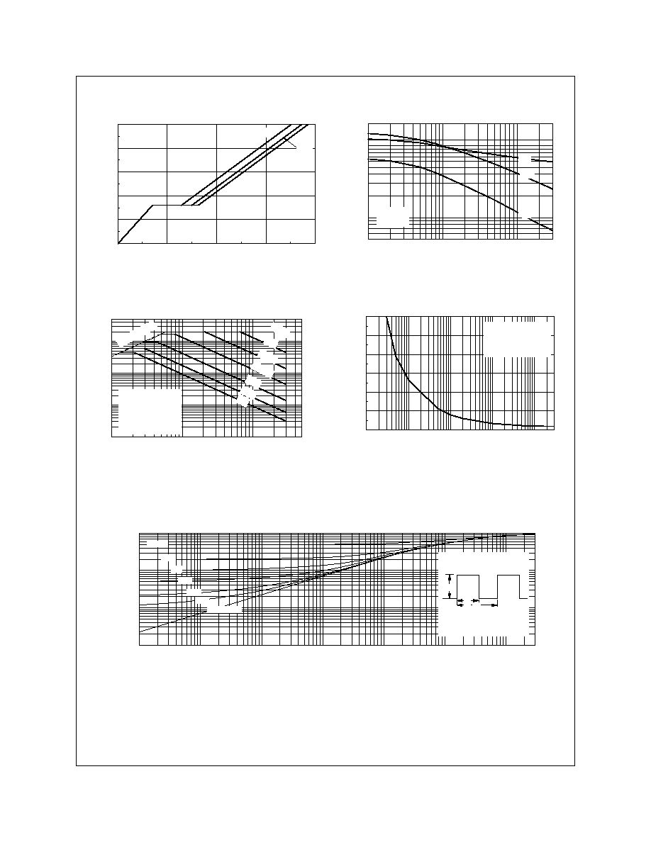
FDS8936A Rev.B
0
5
10
15
20
0
2
4
6
8
10
Q , GATE CHARGE (nC)
V , GATE-SOURCE VOLTAGE (V)
g
GS
I = 6A
D
V = 5V
DS
10V
20V
0.1
0.2
0.5
1
2
5
10
30
50
0.01
0.05
0.1
0.5
1
2
5
10
30
50
V , DRAIN-SOURCE VOLTAGE (V)
I , DRAIN CURRENT (A)
RDS(ON) LIMIT
D
A
DC
DS
1s
100ms
10ms
1ms
10s
V =10V
SINGLE PULSE
R = 135 ∞C/W
T = 25∞C
JA
GS
A
100us
0.01
0.1
0.5
1
10
50 100
300
0
5
10
15
20
25
30
SINGLE PULSE TIME (SEC)
POWER (W)
SINGLE PULSE
R =135∞ C/W
T = 25∞C
JA
A
Figure 10. Single Pulse Maximum Power
Dissipation.
0.1
0.2
0.5
1
2
5
10
30
50
100
200
400
800
1200
2000
V , DRAIN TO SOURCE VOLTAGE (V)
CAPACITANCE (pF)
DS
C
iss
f = 1 MHz
V = 0 V
GS
C
oss
C
rss
Figure 8. Capacitance Characteristics.
Figure 7. Gate Charge Characteristics.
Figure 9. Maximum Safe Operating Area
.
Typical Electrical Characteristics
(continued)
0.0001
0.001
0.01
0.1
1
10
100
300
0.001
0.002
0.005
0.01
0.02
0.05
0.1
0.2
0.5
1
t , TIME (sec)
TRANSIENT THERMAL RESISTANCE
r(t), NORMALIZED EFFECTIVE
1
Single Pulse
D = 0.5
0.1
0.05
0.02
0.01
0.2
Duty Cycle, D = t /t
1 2
R (t) = r(t) * R
R =135 ∞C/W
JA
JA
JA
T - T = P * R (t)
JA
A
J
P(pk)
t
1
t
2
Figure 11. Transient Thermal Response Curve.
Thermal characterization performed using the conditions described in Note 1c. Transient
thermal response will change depending on the circuit board design.