 | –≠–ª–µ–∫—Ç—Ä–æ–Ω–Ω—ã–π –∫–æ–º–ø–æ–Ω–µ–Ω—Ç: FDS8958A | –°–∫–∞—á–∞—Ç—å:  PDF PDF  ZIP ZIP |
Document Outline
- Main Menu
- Discrete
- MOSFETs
- SO-8
- Search
- fairchildsemi.com

January 2001
2001 Fairchild Semiconductor International
FDS8958A Rev D(W)
FDS8958A
Dual N & P-Channel PowerTrench
MOSFET
General Description
These dual N- and P-Channel enhancement mode
power field effect transistors are produced using
Fairchild Semiconductor's advanced PowerTrench
process that has been especially tailored to minimize
on-state ressitance and yet maintain superior switching
performance.
These devices are well suited for low voltage and
battery powered applications where low in-line power
loss and fast switching are required.
Features
∑
Q1:
N-Channel
7.0A,
30V
R
DS(on)
= 0.028
@ V
GS
= 10V
R
DS(on)
= 0.040
@ V
GS
= 4.5V
∑
Q2:
P-Channel
-5A,
-30V
R
DS(on)
= 0.052
@ V
GS
= -10V
R
DS(on)
= 0.080
@ V
GS
= -4.5V
∑
Fast
switching
speed
∑
High power and handling capability in a widely
used surface mount package
S
D
S
S
SO-8
D
D
D
G
D1
D1
D2
D2
S1
G1
S2
G2
Pin 1
SO-8
4
3
2
1
5
6
7
8
Q1
Q2
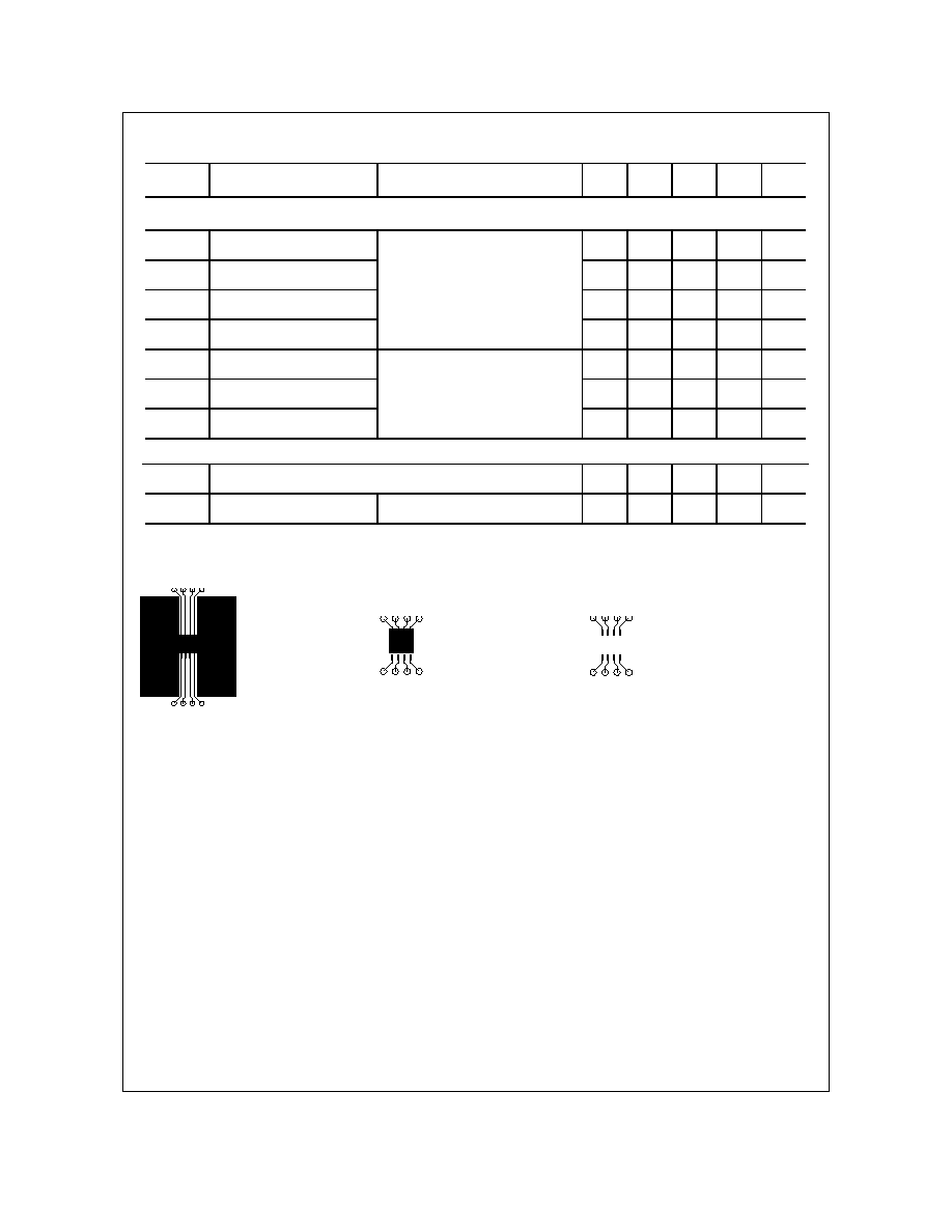
Absolute Maximum Ratings
T
A
= 25∞C unless otherwise noted
Symbol
Parameter
Q1
Q2
Units
V
DSS
Drain-Source Voltage
30
30
V
V
GSS
Gate-Source Voltage
±
20
±
20
V
I
D
Drain Current - Continuous
(Note 1a)
7
-5
A
- Pulsed
20
-20
P
D
Power Dissipation for Dual Operation
2
W
Power Dissipation for Single Operation
(Note 1a)
1.6
(Note 1b)
1
(Note 1c)
0.9
T
J
, T
STG
Operating and Storage Junction Temperature Range
-55 to +150
∞
C
Thermal Characteristics
R
JA
Thermal Resistance, Junction-to-Ambient
(Note 1a)
78
∞
C/W
R
JC
Thermal Resistance, Junction-to-Case
(Note 1)
40
∞
C/W
Package Marking and Ordering Information
Device Marking
Device
Reel Size
Tape width
Quantity
FDS8958A
FDS8958A
13"
12mm
2500 units
FDS8958
A

FDS8958A Rev D(W)
Electrical Characteristics
T
A
= 25∞C unless otherwise noted
Symbol
Parameter
Test Conditions
Type Min Typ Max Units
Off Characteristics
BV
DSS
Drain-Source Breakdown
Voltage
V
GS
= 0 V, I
D
= 250
µ
A
V
GS
= 0 V, I
D
= -250
µ
A
Q1
Q2
30
-30
V
BV
DSS
T
J
Breakdown Voltage
Temperature Coefficient
I
D
= 250
µ
A, Referenced to 25
∞
C
I
D
= -250 µA, Referenced to 25
∞
C
Q1
Q2
25
-22
mV/
∞
C
I
DSS
Zero Gate Voltage Drain
Current
V
DS
= 24 V, V
GS
= 0 V
V
DS
= -24 V, V
GS
= 0 V
Q1
Q2
1
-1
µ
A
I
GSSF
Gate-Body Leakage, Forward V
GS
= 20 V, V
DS
= 0 V
All
100
nA
I
GSSR
Gate-Body Leakage, Reverse V
GS
= -20 V, V
DS
= 0 V
All
-100
nA
On Characteristics
(Note 2)
V
GS(th)
Gate Threshold Voltage
V
DS
= V
GS
, I
D
= 250
µ
A
V
DS
= V
GS
, I
D
= -250 µA
Q1
Q2
1
-1
1.6
-1.7
3
-3
V
V
GS(th)
T
J
Gate Threshold Voltage
Temperature Coefficient
I
D
= 250
µ
A, Referenced to 25
∞
C
I
D
= -250 µA, Referenced to 25
∞
C
Q1
Q2
-4.3
4
mV/
∞
C
V
GS
= 10 V, I
D
= 7 A
V
GS
= 10 V, I
D
= 7 A, T
J
= 125
∞
C
V
GS
= 4.5 V, I
D
= 6 A
Q1
21
32
27
28
42
40
m
R
DS(on)
Static Drain-Source
On-Resistance
V
GS
= -10 V, I
D
= -5 A
V
GS
= -10 V, I
D
= -5 A, T
J
= 125
∞
C
V
GS
= -4.5 V, I
D
= -4 A
Q2
41
58
58
52
78
80
I
D(on)
On-State Drain Current
V
GS
= 10 V, V
DS
= 5 V
V
GS
= -10 V, V
DS
= -5 V
Q1
Q2
20
-20
A
g
FS
Forward Transconductance
V
DS
= 5 V, I
D
= 7 A
V
DS
= -5 V, I
D
=-5 A
Q1
Q2
19
11
S
Dynamic Characteristics
C
iss
Input Capacitance
Q1
Q2
789
690
pF
C
oss
Output Capacitance
Q1
Q2
173
306
pF
C
rss
Reverse Transfer Capacitance
Q1
V
DS
= 10 V, V
GS
= 0 V, f = 1.0 MHz
Q2
V
DS
= -10 V, V
GS
= 0 V, f = 1.0 MHz
Q1
Q2
66
77
pF
FDS8958
A
FDS8958A Rev D(W)
Electrical Characteristics
(continued)
T
A
= 25∞C unless otherwise noted
Symbol
Parameter
Test Conditions
Type Min
Typ Max Units
Switching Characteristics
(Note 2)
t
d(on)
Turn-On Delay Time
Q1
Q2
2.2
6.7
4.4
13.4
ns
t
r
Turn-On Rise Time
Q1
Q2
7.5
9.7
15
19.4
ns
t
d(off)
Turn-Off Delay Time
Q1
Q2
11.8
19.8
21.3
35.6
ns
t
f
Turn-Off Fall Time
Q1
V
DD
= 10 V, I
D
= 1 A,
V
GS
= 10V, R
GEN
= 6
Q2
V
DD
= -10 V, I
D
= -1 A,
V
GS
= -10V, R
GEN
= 6
Q1
Q2
3.7
12.3
7.4
22.2
ns
Q
g
Total Gate Charge
Q1
Q2
16
14
26
23
nC
Q
gs
Gate-Source Charge
Q1
Q2
2.5
2.4
nC
Q
gd
Gate-Drain Charge
Q1
V
DS
= 15 V, I
D
= 7 A, V
GS
= 10 V
Q2
V
DS
= -15 V, I
D
= -5 A,V
GS
= -10 V
Q1
Q2
2.6
4.8
nC
Drain≠Source Diode Characteristics and Maximum Ratings
I
S
Maximum Continuous Drain-Source Diode Forward Current
Q1
Q2
1.3
-1.3
A
V
SD
Drain-Source Diode Forward
Voltage
V
GS
= 0 V, I
S
= 1.3 A
(Note
2)
V
GS
= 0 V, I
S
= -1.3 A
(Note
2)
Q1
Q2
0.74
-0.76
1.2
-1.2
V
Notes:
1. R
JA
is the sum of the junction-to-case and case-to-ambient thermal resistance where the case thermal reference is defined as the solder mounting surface of
the drain pins. R
JC
is guaranteed by design while R
CA
is determined by the user's board design.
a) 78∞/W when
mounted on a
0.5 in
2
pad of 2 oz
copper
b) 125∞/W when
mounted on a .02 in
2
pad of 2 oz copper
c) 135∞/W when mounted on a
minimum pad.
Scale 1 : 1 on letter size paper
2. Pulse Test: Pulse Width < 300
µ
s, Duty Cycle < 2.0%

FDS8958A Rev D(W)
Typical Characteristics: Q1
0
10
20
30
0
1
2
3
4
5
V
DS
, DRAIN-SOURCE VOLTAGE (V)
4.0V
3.5V
3.0V
2.5V
V
GS
= 10V
5.0V
7.0V
4.5V
0.8
1.0
1.2
1.4
1.6
1.8
2.0
2.2
2.4
0
6
12
18
24
30
I
D
, DRAIN CURRENT (A)
V
GS
= 3.0V
5.0V
7.0V
10V
4.0V
3.5V
4.5V
6.0V
Figure 1. On-Region Characteristics.
Figure 2. On-Resistance Variation with
Drain Current and Gate Voltage.
0.4
0.7
1.0
1.3
1.6
1.9
-50
-25
0
25
50
75
100
125
150
T
J
, JUNCTION TEMPERATURE (
o
C)
I
D
= 7A
V
GS
= 10V
0.01
0.02
0.03
0.04
0.05
0.06
0.07
0.08
0.09
2
4
6
8
10
V
GS
, GATE TO SOURCE VOLTAGE (V)
I
D
= 7A
T
A
= 125
o
C
T
A
= 25
o
C
Figure 3. On-Resistance Variation with
Temperature.
Figure 4. On-Resistance Variation with
Gate-to-Source Voltage.
0
5
10
15
20
25
30
1
2
3
4
5
V
GS
, GATE TO SOURCE VOLTAGE (V)
T
A
= -55
o
C
25
o
C
125
o
C
V
DS
= 10V
0.001
0.01
0.1
1
10
100
0
0.2
0.4
0.6
0.8
1
1.2
1.4
V
SD
, BODY DIODE FORWARD VOLTAGE (V)
T
A
= 125
o
C
25
o
C
-55
o
C
V
GS
= 0V
Figure 5. Transfer Characteristics.
Figure 6. Body Diode Forward Voltage Variation
with Source Current and Temperature.
FDS8958
A

FDS8958A Rev D(W)
Typical Characteristics: Q1
0
2
4
6
8
10
0
4
8
12
16
Q
g
, GATE CHARGE (nC)
I
D
=7A
V
DS
= 5V
15V
10V
0
300
600
900
1200
0.0
5.0
10.0
15.0
20.0
V
DS
, DRAIN TO SOURCE VOLTAGE (V)
C
ISS
C
RSS
C
OSS
f = 1MHz
V
GS
= 0 V
Figure 7. Gate Charge Characteristics.
Figure 8. Capacitance Characteristics.
0.01
0.1
1
10
100
0.1
1
10
100
V
DS
, DRAIN-SOURCE VOLTAGE (V)
DC
10s
1s
100ms
100
µ
s
R
DS(ON)
LIMIT
V
GS
= 10V
SINGLE PULSE
R
JA
= 135
o
C/W
T
A
= 25
o
C
10ms
1ms
0
10
20
30
40
50
0.001
0.01
0.1
1
10
100
1000
t
1
, TIME (sec)
SINGLE PULSE
R
JA
= 135∞C/W
T
A
= 25∞C
Figure 9. Maximum Safe Operating Area.
Figure 10. Single Pulse Maximum
Power Dissipation.
FDS8958
A