 | –≠–ª–µ–∫—Ç—Ä–æ–Ω–Ω—ã–π –∫–æ–º–ø–æ–Ω–µ–Ω—Ç: FDU6030BL | –°–∫–∞—á–∞—Ç—å:  PDF PDF  ZIP ZIP |
July 2001
©
2001 Fairchild Semiconductor Corporation
FDD6030BL/FDU6030BL Rev C(W)
FDD6030BL/FDU6030BL
30V N-Channel PowerTrench
Æ
Æ
MOSFET
General Description
This N-Channel MOSFET has been designed
specifically to improve the overall efficiency of DC/DC
converters using either synchronous or conventional
switching PWM controllers. It has been optimized for
low gate charge, low R
DS( ON)
, fast switching speed and
extremely low R
DS(ON)
in a small package.
Applications
∑
DC/DC converter
∑
Motor drives
Features
∑
42 A, 30 V
R
DS(ON)
= 16 m
@ V
GS
= 10 V
R
DS(ON)
= 22 m
@ V
GS
= 4.5 V
∑
Low gate charge (22 nC typical)
∑
Fast switching
∑
High performance trench technology for extremely
low R
DS(ON)
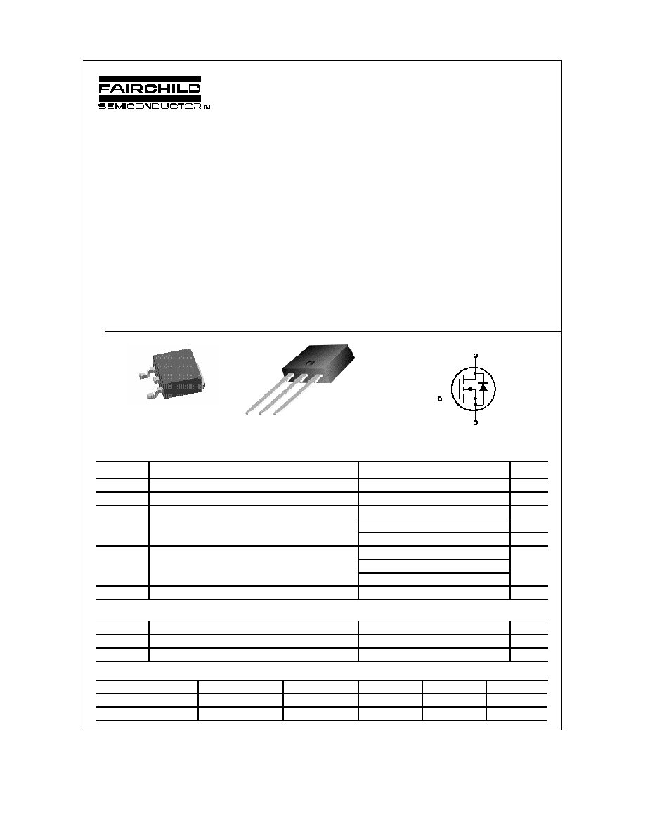
G
S
D
TO-252
D-PAK
(TO-252)
G D S
I-PAK
(TO-251AA)
S
G
D
Absolute Maximum Ratings
T
A
=25
o
C unless otherwise noted
Symbol
Parameter
Ratings
Units
V
DSS
Drain-Source Voltage
30
V
V
GSS
Gate-Source Voltage
±
20
V
I
D
Continuous Drain Current @T
C
=25∞C
(Note 3)
42
A
@T
A
=25∞C
(Note 1a)
10
Pulsed
(Note 1a)
100
Power Dissipation
@T
C
=25∞C
(Note 3)
50
@T
A
=25∞C
(Note 1a)
3.8
P
D
@T
A
=25∞C
(Note 1b)
1.6
W
T
J
, T
STG
Operating and Storage Junction Temperature Range
≠55 to +175
∞
C
Thermal Characteristics
R
JC
Thermal Resistance, Junction-to-Case
(Note 1)
3.0
∞
C/W
R
JA
Thermal Resistance, Junction-to-Ambient
(Note 1a)
45
∞
C/W
R
JA
Thermal Resistance, Junction-to-Ambient
(Note 1b)
96
∞
C/W
Package Marking and Ordering Information
Device Marking
Device
Package
Reel Size
Tape width
Quantity
FDD6030BL
FDD6030BL
D-PAK (TO-252)
13''
12mm
2500 units
FDU6030BL
FDU6030BL
I-PAK (TO-251)
Tube
N/A
75
FDD6030BL/FDU6030BL
FDD6030BL/FDU6030BL Rev. C(W)
Electrical Characteristics
T
A
= 25∞C unless otherwise noted
Symbol
Parameter
Test Conditions
Min Typ Max Units
Drain-Source Avalanche Ratings
(Note 2)
W
DSS
Drain-Source Avalanche Energy
Single Pulse, V
DD
= 15 V
130
mJ
I
AR
Drain-Source Avalanche Current
10
A
Off Characteristics
BV
DSS
Drain≠Source Breakdown Voltage V
GS
= 0 V, I
D
= 250
µ
A
30
V
BV
DSS
T
J
Breakdown Voltage Temperature
Coefficient
I
D
= 250
µ
A,Referenced to 25
∞
C
22
mV/
∞
C
I
DSS
Zero Gate Voltage Drain Current
V
DS
= 24 V, V
GS
= 0 V
1
µ
A
I
GSSF
Gate≠Body Leakage, Forward
V
GS
= 20 V, V
DS
= 0 V
100
nA
I
GSSR
Gate≠Body Leakage, Reverse
V
GS
= ≠20 V, V
DS
= 0 V
≠100
nA
On Characteristics
(Note 2)
V
GS(th)
Gate Threshold Voltage
V
DS
= V
GS
, I
D
= 250
µ
A
1
1.6
3
V
V
GS(th)
T
J
Gate Threshold Voltage
Temperature Coefficient
I
D
= 250
µ
A, Referenced to 25
∞
C
≠4
mV/
∞
C
R
DS(on)
Static Drain≠Source
On≠Resistance
V
GS
= 10 V, I
D
= 10 A
V
GS
= 4.5 V, I
D
= 8.4 A
V
GS
= 10 V, I
D
= 10 A, T
J
=125
∞
C
12
17
19
16
22
26
m
I
D(on)
On≠State Drain Current
V
GS
= 10 V, V
DS
= 5 V
50
A
g
FS
Forward Transconductance
V
DS
= 10 V, I
D
= 10 A
29
S
Dynamic Characteristics
C
iss
Input Capacitance
1143
pF
C
oss
Output Capacitance
249
pF
C
rss
Reverse Transfer Capacitance
V
DS
= 15 V,
V
GS
= 0 V,
f = 1.0 MHz
107
pF
Switching Characteristics
(Note 2)
t
d(on)
Turn≠On Delay Time
6
12
ns
t
r
Turn≠On Rise Time
10
18
ns
t
d(off)
Turn≠Off Delay Time
18
29
ns
t
f
Turn≠Off Fall Time
V
DD
= 15 V,
I
D
= 1 A,
V
GS
= 10 V,
R
GEN
= 6
5
12
ns
Q
g
Total Gate Charge
22
31
nC
Q
gs
Gate≠Source Charge
3
nC
Q
gd
Gate≠Drain Charge
V
DS
= 15V,
I
D
= 10 A,
V
GS
= 10 V
4
nC
FDD6030BL/FDU6030BL
FDD6030BL/FDU6030BL Rev. C(W)
D
R
P
DS(ON)
Electrical Characteristics
T
A
= 25∞C unless otherwise noted
Symbol
Parameter
Test Conditions
Min Typ Max Units
Drain≠Source Diode Characteristics and Maximum Ratings
I
S
Maximum Continuous Drain≠Source Diode Forward Current
3.2
A
V
SD
Drain≠Source Diode Forward
Voltage
V
GS
= 0 V, I
S
= 3.2 A
(Note 2)
0.7
1.2
V
Notes:
1. R
JA
is the sum of the junction-to-case and case-to-ambient thermal resistance where the case thermal reference is defined as the solder mounting surface of
the drain pins. R
JC
is guaranteed by design while R
CA
is determined by the user's board design.
a) R
JA
= 45∞C/W when mounted on a
1in
2
pad of 2 oz copper
b) R
JA
= 96∞C/W when mounted
on a minimum pad.
Scale 1 : 1 on letter size paper
2. Pulse Test: Pulse Width < 300
µ
s, Duty Cycle < 2.0%
3. Maximum current is calculated as:
where P
D
is maximum power dissipation at T
C
= 25∞C and R
DS(on)
is at T
J(max)
and V
GS
= 10V. Package current limitation is 21A
FDD6030BL/FDU6030BL
FDD6030BL/FDU6030BL Rev. C(W)
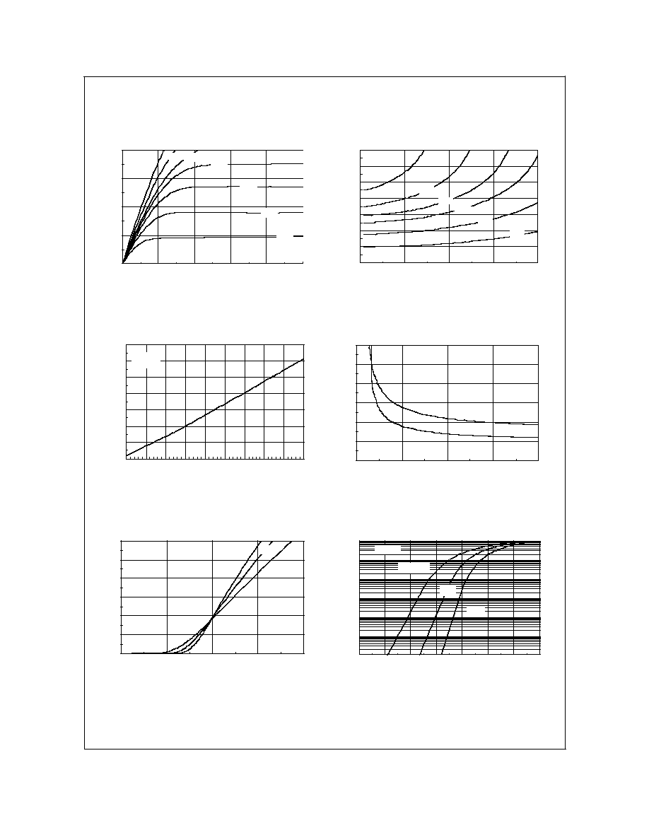
Typical Characteristics
0
20
40
60
80
0
1
2
3
4
5
V
DS
, DRAIN-SOURCE VOLTAGE (V)
I
D
, DRAIN CURRENT (A)
6.0V
5.0V
V
GS
= 10V
4.5V
4.0V
3.5V
3.0V
0.8
1
1.2
1.4
1.6
1.8
2
2.2
0
20
40
60
80
I
D
, DRAIN CURRENT (A)
R
DS(ON)
, NORMALIZED
DRAIN-SOURCE ON-RESISTANCE
V
GS
= 3.5V
4.0V
5.0V
6.0V
4.5V
10V
Figure 1. On-Region Characteristics
Figure 2. On-Resistance Variation with
Drain Current and Gate Voltage
0.6
0.8
1
1.2
1.4
1.6
1.8
2
-50
-25
0
25
50
75
100
125
150
175
T
J
, JUNCTION TEMPERATURE (
o
C)
R
DS(ON)
, NORMALIZED
DRAIN-SOURCE ON-RESISTANCE
I
D
= 10A
V
GS
= 10V
0
0.01
0.02
0.03
0.04
0.05
0.06
2
4
6
8
10
V
GS
, GATE TO SOURCE VOLTAGE (V)
R
DS(ON)
, ON-RESISTANCE (OHM)
I
D
= 5A
T
A
= 125
o
C
T
A
= 25
o
C
Figure 3. On-Resistance Variation with
Temperature
Figure 4. On-Resistance Variation with
Gate-to-Source Voltage
0
10
20
30
40
50
60
1
2
3
4
5
V
GS
, GATE TO SOURCE VOLTAGE (V)
I
D
, DRAIN CURRENT (A)
T
A
=-55
o
C
25
o
C
125
o
C
V
DS
= 5V
0.0001
0.001
0.01
0.1
1
10
100
0
0.2
0.4
0.6
0.8
1
1.2
1.4
V
SD
, BODY DIODE FORWARD VOLTAGE (V)
I
S
, REVERSE DRAIN CURRENT (A)
T
A
= 125
o
C
25
o
C
-55
o
C
V
GS
= 0V
Figure 5. Transfer Characteristics
Figure 6. Body Diode Forward Voltage Variation
with Source Current and Temperature
FDD6030BL/FDU6030BL

FDD6030BL/FDU6030BL Rev. C(W)
Typical Characteristics
0
2
4
6
8
10
0
4
8
12
16
20
24
Q
g
, GATE CHARGE (nC)
V
GS
, GATE-SOURCE VOLTAGE (V)
I
D
= 10A
V
DS
= 5V
15V
10V
0
400
800
1200
1600
0
5
10
15
20
25
30
V
DS
, DRAIN TO SOURCE VOLTAGE (V)
CAPACITANCE (pF)
C
ISS
C
RSS
C
OSS
f = 1MHz
V
GS
= 0 V
Figure 7. Gate Charge Characteristics
Figure 8. Capacitance Characteristics
0.01
0.1
1
10
100
1000
0.01
0.1
1
10
100
V
DS
, DRAIN-SOURCE VOLTAGE (V)
I
D
, DRAIN CURRENT (A)
DC
1s
100ms
R
DS(ON)
LIMIT
V
GS
= 10V
SINGLE PULSE
R
JA
= 96
o
C/W
T
A
= 25
o
C
10ms
1m
100µs
10s
0
20
40
60
80
100
0.01
0.1
1
10
100
1000
t
1
, TIME (sec)
P(pk), PEAK TRANSIENT POWER (W)
SINGLE PULSE
R
JA
= 96∞C/W
T
A
= 25∞C
Figure 9. Maximum Safe Operating Area
Figure 10. Single Pulse Maximum
Power Dissipation
0.001
0.01
0.1
1
0.001
0.01
0.1
1
10
100
1000
r(t), NORMALIZED EFFECTIVE
TRANSIENT THERMAL RESISTANCE
R
JA
(t) = r(t) + R
JA
R
JA
= 96 ∞C/W
T
J
- T
A
= P * R
JA
(t)
Duty Cycle, D = t
1
/ t
2
P(pk)
t
1
t
2
SINGLE PULSE
0.01
0.02
0.05
0.1
0.2
D = 0.5
Figure 11. Transient Thermal Response Curve
Thermal characterization performed using the conditions described in Note 1b.
Transient thermal response will change depending on the circuit board design.
FDD6030BL/FDU6030BL