Äîêóìåíòàöèÿ è îïèñàíèÿ www.docs.chipfind.ru
March 2006
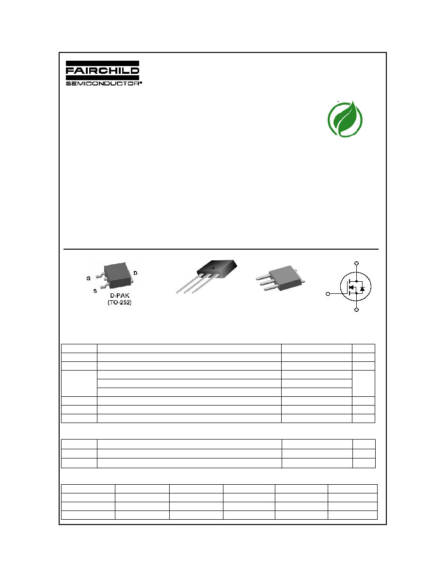
FDD8796/FDU8796 N-Channel PowerTrench
®
MOSFET
©2006 Fairchild Semiconductor Corporation
FDD8796/FDU8796 Rev. B
www.fairchildsemi.com
1
FDD8796/FDU8796
N-Channel PowerTrench
®
MOSFET
25V, 35A, 5.7m
General Description
This N-Channel MOSFET has been designed specifically to
improve the overall efficiency of DC/DC converters using
either synchronous or conventional switching PWM
controllers. It has been optimized for low gate charge, low
r
DS(on)
and fast switching speed.
Application
Vcore DC-DC for Desktop Computers and Servers
VRM for Intermediate Bus Architecture
Features
Max r
DS(on)
= 5.7m
at V
GS
= 10V, I
D
= 35A
Max r
DS(on)
= 8.0m
at V
GS
= 4.5V, I
D
= 35A
Low gate charge: Q
g(10)
= 37nC(Typ), V
GS
= 10V
Low gate resistance
Avalanche rated and 100% tested
RoHS Compliant
D
G
S
Short Lead I-PAK
I-PAK
(TO-251AA)
G D S
G
D
S
MOSFET Maximum Ratings
T
C
= 25°C unless otherwise noted
Thermal Characteristics
Package Marking and Ordering Information
Symbol
Parameter
Ratings
Units
V
DS
Drain to Source Voltage
25
V
V
GS
Gate to Source Voltage
±20
V
I
D
Drain Current -Continuous (Package Limited)
35
A
-Continuous (Die Limited)
98
-Pulsed (Note 1)
305
E
AS
Single Pulse Avalanche Energy (Note 2)
91
mJ
P
D
Power Dissipation
88
W
T
J
, T
STG
Operating and Storage Temperature
-55 to 175
°C
R
JC
Thermal Resistance, Junction to Case TO_252, TO_251
1.7
°C/W
R
JA
Thermal Resistance, Junction to Ambient TO_252, TO_251
100
°C/W
R
JA
Thermal Resistance, Junction to Ambient TO-252,1in
2
copper pad area
52
°C/W
Device Marking
Device
Package
Reel Size
Tape Width
Quantity
FDD8796
FDD8796
TO-252AA
13''
12mm
2500 units
FDU8796
FDU8796
TO-251AA
N/A (Tube)
N/A
75 units
FDU8796
FDU8796_F071
TO-251AA
N/A (Tube)
N/A
75 units
L
E
A D
F R E E
M
T
A
E
L
N
TI
O
MP
E
N
I
FDD8796/FDU8796 N-Channel PowerTrench
®
MOSFET
FDD8796/FDU8796 Rev. B
2
www.fairchildsemi.com
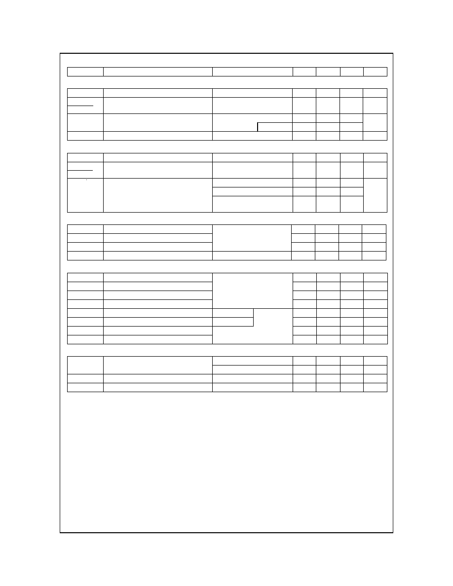
Electrical Characteristics
T
J
= 25°C unless otherwise noted
Symbol
Parameter
Test Conditions
Min
Typ
Max
Units
Off Characteristics
B
VDSS
Drain to Source Breakdown Voltage
I
D
= 250
µA, V
GS
= 0V
25
V
B
VDSS
T
J
Breakdown Voltage Temperature
Coefficient
I
D
= 250
µA, referenced to
25°C
7
mV/°C
I
DSS
Zero Gate Voltage Drain Current
V
DS
= 20V
V
GS
= 0V T
J
= 150°C
1
µA
250
I
GSS
Gate to Source Leakage Current
V
GS
= ±20V
±100
nA
On Characteristics
V
GS(th)
Gate to Source Threshold Voltage
V
GS
= V
DS
, I
D
= 250
µA
1.2
1.8
2.5
V
V
GS(th)
T
J
Gate to Source Threshold Voltage
Temperature Coefficient
I
D
= 250
µA, referenced to
25°C
-6.7
mV/°C
r
DS(on)
Drain to Source On Resistance
V
GS
= 10V, I
D
= 35A
4.5
5.7
m
V
GS
= 4.5V, I
D
= 35A
6.0
8.0
V
DS
= 10V, I
D
= 35A
T
J
= 175°C
6.9
9.5
Dynamic Characteristics
C
iss
Input Capacitance
V
DS
= 13V, V
GS
= 0V,
f = 1MHz
1960
2610
pF
C
oss
Output Capacitance
455
605
pF
C
rss
Reverse Transfer Capacitance
315
475
pF
R
G
Gate Resistance
f = 1MHz
1.1
Switching Characteristics
t
d(on)
Turn-On Delay Time
V
DD
=13V, I
D
= 35A
V
GS
= 10V, R
GS
= 20
10
20
ns
t
r
Rise Time
24
39
ns
t
d(off)
Turn-Off Delay Time
99
158
ns
t
f
Fall Time
57
91
ns
Q
g
Total Gate Charge
V
GS
= 0 to10V
V
DD
=13V,
I
D
= 35A,
I
g
= 1.0mA
37
52
nC
Q
g
Total Gate Charge
V
GS
= 0 to 5V
19
27
nC
Q
gs
Gate to Source Gate Charge
6
nC
Q
gd
Gate to Drain Charge
6
nC
Drain-Source Diode Characteristics
V
SD
Source to Drain Diode Voltage
V
GS
= 0V, I
S
= 35A
0.9
1.25
V
V
GS
= 0V, I
S
= 15A
0.8
1.0
V
t
rr
Reverse Recovery Time
I
F
= 35A, di/dt = 100A/
µs
30
45
ns
Q
rr
Reverse Recovery Charge
I
F
= 35A, di/dt = 100A/
µs
23
35
nC
Notes:
1: Pulse time < 300
µs, Duty cycle = 2%.
2: Starting T
J
= 25°C, L = 0.3mH, I
AS
= 24.7A, V
DD
= 23V, V
GS
= 10V.
FDD8796/FDU8796 N-Channel PowerTrench
®
MOSFET
FDD8796/FDU8796 Rev. B
3
www.fairchildsemi.com
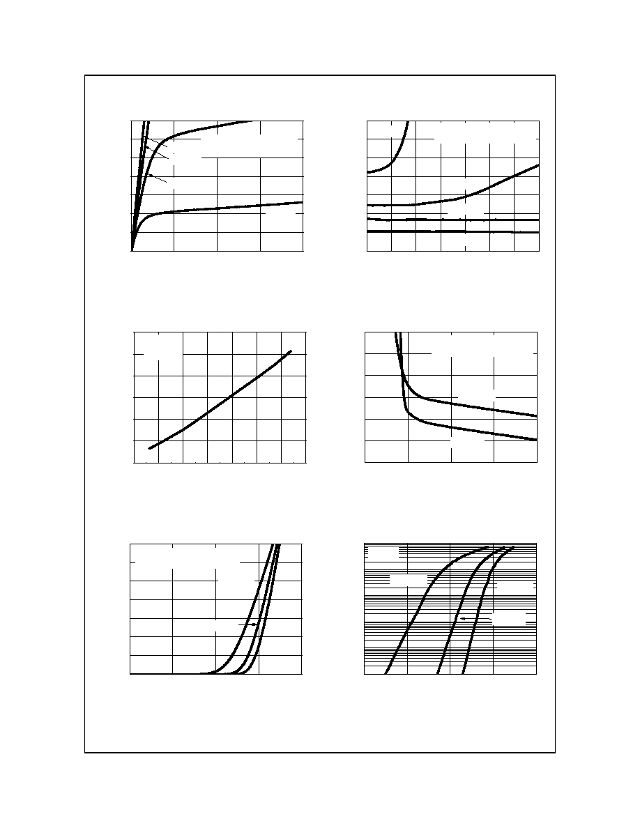
Typical Characteristics
T
J
= 25°C unless otherwise noted
Figure 1. On Region Characteristics
0
1
2
3
4
0
10
20
30
40
50
60
70
V
GS
= 3.5V
PULSE DURATION = 80
µ
s
DUTY CYCLE = 0.5%MAX
V
GS
= 3V
V
GS
= 4.5V
V
GS
= 10V
I
D
, DR
AI
N CUR
RE
N
T
(
A
)
V
DS
, DRAIN TO SOURCE VOLTAGE (V)
Figure 2. Normalized
0
10
20
30
40
50
60
70
0.5
1.0
1.5
2.0
2.5
3.0
3.5
4.0
V
GS
= 3V
PULSE DURATION = 80
µ
s
DUTY CYCLE = 0.5%MAX
NOR
M
ALIZED
DR
AIN
TO SOUR
C
E
ON-R
ESISTA
N
CE
I
D
, DRAIN CURRENT(A)
V
GS
=
10V
V
GS
= 4.5V
V
GS
= 3.5V
On-Resistance vs Drain
Current and Gate Voltage
Figure 3.
-80
-40
0
40
80
120
160
200
0.6
0.8
1.0
1.2
1.4
1.6
1.8
T
J
, JUNCTION TEMPERATURE (
o
C)
NO
R
M
AL
IZ
E
D
DR
AI
N TO
S
O
UR
CE
O
N
-
R
E
S
I
S
T
AN
CE
I
D
= 35A
V
GS
= 10V
Normalized On Resistance vs Junction
Temperature
Figure 4.
2
4
6
8
10
2
4
6
8
10
12
14
PULSE DURATION = 80
µ
s
DUTY CYCLE = 0.5%MAX
T
J
= 175
o
C
T
J
= 25
o
C
I
D
=35A
r
D
S
(
on)
, O
N
-R
ESI
STAN
CE
(
m
)
V
GS
, GATE TO SOURCE VOLTAGE (V)
On-Resistance vs Gate to Source
Voltage
Figure 5. Transfer Characteristics
0
1
2
3
4
0
10
20
30
40
50
60
70
PULSE DURATION = 80
µ
s
DUTY CYCLE = 0.5%MAX
T
J
= -55
o
C
T
J
= 25
o
C
T
J
= 175
o
C
I
D
,
DRA
I
N
CU
RR
E
NT
(
A)
V
GS
, GATE TO SOURCE VOLTAGE (V)
Figure 6.
0.0
0.3
0.6
0.9
1.2
1E-3
0.01
0.1
1
10
100
T
J
= -55
o
C
T
J
= 25
o
C
T
J
= 175
o
C
V
GS
= 0V
I
S
,
REVER
SE D
R
A
I
N
C
U
R
R
E
NT (A
)
V
SD
, BODY DIODE FORWARD VOLTAGE (V)
Source to Drain Diode Forward
Voltage vs Source Current
FDD8796/FDU8796 N-Channel PowerTrench
®
MOSFET
FDD8796/FDU8796 Rev. B
4
www.fairchildsemi.com
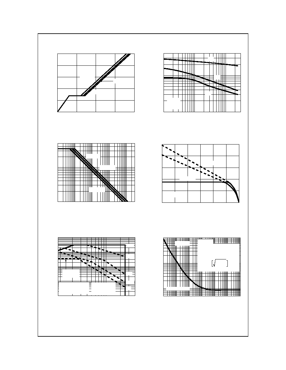
Figure 7.
0
10
20
30
40
0
2
4
6
8
10
V
DD
= 16V
V
DD
= 10V
V
GS
,
G
A
T
E TO
SO
U
R
C
E VO
L
T
AG
E(V)
Q
g
, GATE CHARGE(nC)
V
DD
= 13V
Gate Charge Characteristics
Figure 8.
0.1
1
10
100
1000
f = 1MHz
V
GS
= 0V
CA
PA
CITA
NC
E (pF)
V
DS
, DRAIN TO SOURCE VOLTAGE (V)
C
rss
C
oss
C
iss
4000
30
Capacitance vs Drain to Source Voltage
Figure 9. Unclamped Inductive Switching
Capability
0.01
0.1
1
10
100
1
10
T
J
= 125
o
C
T
J
= 25
o
C
T
J
= 150
o
C
I
AS
,
AVAL
A
NCHE
CURRENT(
A)
t
AV
, TIME IN AVALANCHE(ms)
50
300
Figure 10.
25
50
75
100
125
150
175
0
20
40
60
80
100
R
JC
=
1.7
o
C/W
I
D
, DRAIN
CURRENT
(
A
)
T
C
, CASE TEMPERATURE(
o
C)
V
GS
= 10V
V
GS
= 4.5V
Maximum Continuous Drain Current vs
Case Temperature
Figure 11.
1
10
0.1
1
10
100
1000
LIMITED BY
PACKAGE
1ms
100us
10ms
10us
DC
I
D
, D
R
AIN
CU
RR
EN
T (A
)
V
DS
, DRAIN TO SOURCE VOLTAGE (V)
SINGLE PULSE
T
J
= MAX RATED
T
C
=
25
o
C
OPERATION IN THIS
AREA MAY BE
LIMITED BY
r
DS(on)
40
Forward Bias Safe Operating Area
Figure 12. Single Pulse Maximum Power
Dissipation
10
-5
10
-4
10
-3
10
-2
10
-1
10
0
10
1
100
1000
10000
SINGLE PULSE
V
GS
= 10V
P
( PK
)
, P
E
A
K
TR
ANS
I
E
NT
P
O
W
E
R (
W
)
t, PULSE WIDTH (s)
50
T
C
= 25
o
C
I = I
25
FOR TEMPERATURES
ABOVE 25
o
C DERATE PEAK
CURRENT AS FOLLOWS:
175 T
C
150
-----------------------
Typical Characteristics
T
J
= 25°C unless otherwise noted
FDD8796/FDU8796 N-Channel PowerTrench
®
MOSFET
FDD8796/FDU8796 Rev. B
5
www.fairchildsemi.com
Figure 13.
10
-5
10
-4
10
-3
10
-2
10
-1
10
0
10
1
1E-3
0.01
0.1
1
DUTY CYCLE-DESENDING ORDER
NO
R
M
AL
IZ
E
D
TH
E
R
M
A
L
IM
PED
AN
CE, Z
JC
t, RECTANGULAR PULSE DURATION(s)
D = 0.5
0.2
0.1
0.05
0.02
0.01
SINGLE PULSE
2
P
DM
t
1
t
2
NOTES:
DUTY FACTOR: D = t
1
/t
2
PEAK T
J
= P
DM
x Z
JC
x R
JC
+ T
C
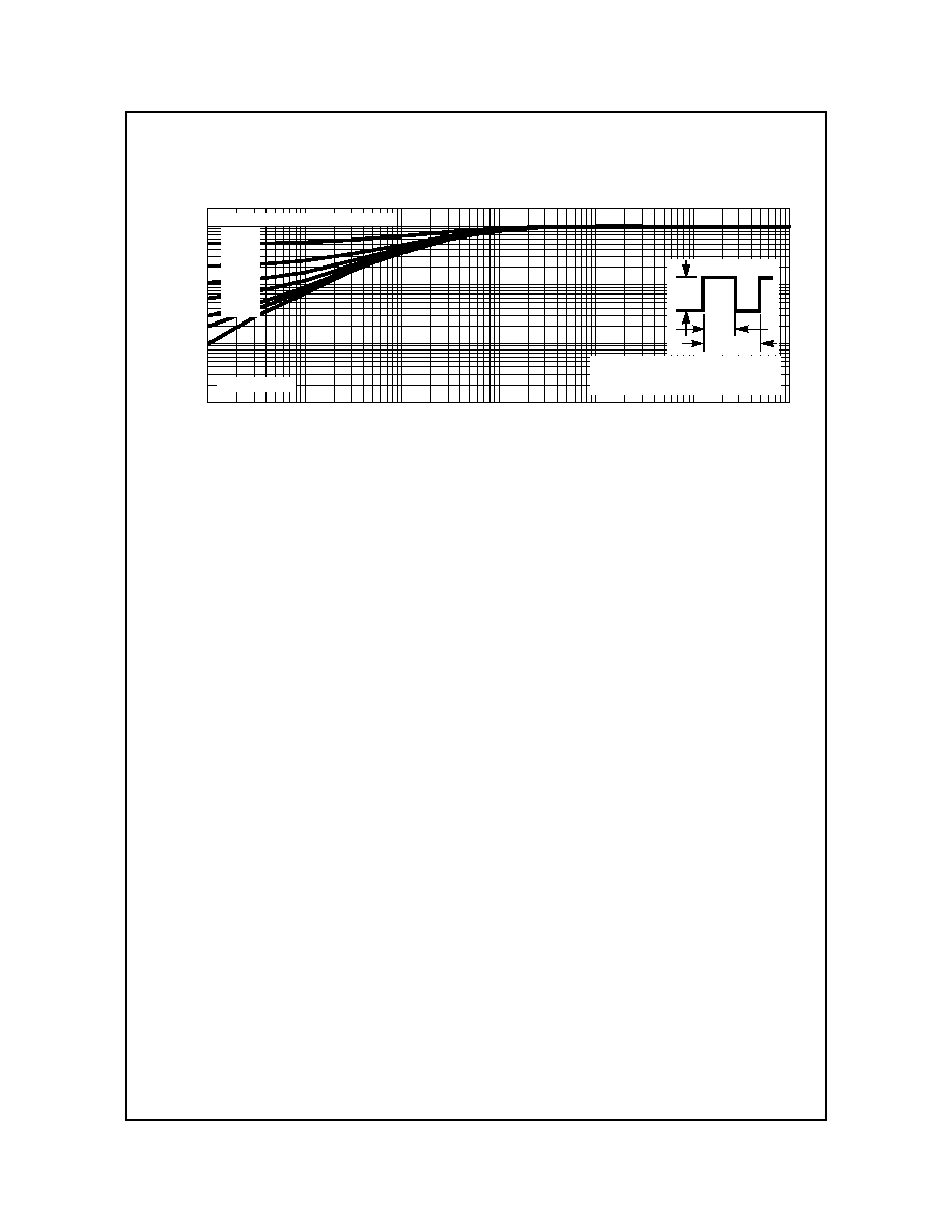
Transient Thermal Response Curve
Typical Characteristics
T
J
= 25°C unless otherwise noted

FDD8796/FDU8796 Rev. B
www.fairchildsemi.com
6
FDD8796/FDU8796 N-Ch
annel PowerTrench
®
MO
SFET
Rev. I18
TRADEMARKS
The following are registered and unregistered trademarks Fairchild Semiconductor owns or is authorized to use and is not
intended to be an exhaustive list of all such trademarks.
DISCLAIMER
FAIRCHILD SEMICONDUCTOR RESERVES THE RIGHT TO MAKE CHANGES WITHOUT FURTHER NOTICE TO ANY
PRODUCTS HEREIN TO IMPROVE RELIABILITY, FUNCTION OR DESIGN. FAIRCHILD DOES NOT ASSUME ANY
LIABILITY ARISING OUT OF THE APPLICATION OR USE OF ANY PRODUCT OR CIRCUIT DESCRIBED HEREIN;
NEITHER DOES IT CONVEY ANY LICENSE UNDER ITS PATENT RIGHTS, NOR THE RIGHTS OF OTHERS.
LIFE SUPPORT POLICY
FAIRCHILD'S PRODUCTS ARE NOT AUTHORIZED FOR USE AS CRITICAL COMPONENTS IN LIFE SUPPORT
DEVICES OR SYSTEMS WITHOUT THE EXPRESS WRITTEN APPROVAL OF FAIRCHILD SEMICONDUCTOR
CORPORATION.
As used herein:
1. Life support devices or systems are devices or systems
which, (a) are intended for surgical implant into the body, or
(b) support or sustain life, or (c) whose failure to perform
when properly used in accordance with instructions for use
provided in the labeling, can be reasonably expected to
result in significant injury to the user.
2. A critical component is any component of a life support
device or system whose failure to perform can be
reasonably expected to cause the failure of the life support
device or system, or to affect its safety or effectiveness.
PRODUCT STATUS DEFINITIONS
Definition of Terms
ACExTM
ActiveArrayTM
BottomlessTM
Build it NowTM
CoolFETTM
CROSSVOLTTM
DOMETM
EcoSPARKTM
E
2
CMOSTM
EnSignaTM
FACTTM
FACT Quiet SeriesTM
FAST
®
FASTrTM
FPSTM
FRFETTM
GlobalOptoisolatorTM
GTOTM
HiSeCTM
I
2
CTM
i-LoTM
ImpliedDisconnectTM
IntelliMAXTM
ISOPLANARTM
LittleFETTM
MICROCOUPLERTM
MicroFETTM
MicroPakTM
MICROWIRETM
MSXTM
MSXProTM
OCXTM
OCXProTM
OPTOLOGIC
®
OPTOPLANARTM
PACMANTM
POPTM
Power247TM
PowerEdgeTM
PowerSaverTM
PowerTrench
®
QFET
®
QSTM
QT OptoelectronicsTM
Quiet SeriesTM
RapidConfigureTM
RapidConnectTM
µSerDesTM
ScalarPumpTM
SILENT SWITCHER
®
SMART STARTTM
SPMTM
StealthTM
SuperFETTM
SuperSOTTM-3
SuperSOTTM-6
SuperSOTTM-8
SyncFETTM
TCMTM
TinyLogic
®
TINYOPTOTM
TruTranslationTM
UHCTM
UltraFET
®
UniFETTM
VCXTM
WireTM
Across the board. Around the world.TM
The Power Franchise
®
Programmable Active DroopTM
Datasheet Identification
Product Status
Definition
Advance Information
Formative or In
Design
This datasheet contains the design specifications for
product development. Specifications may change in
any manner without notice.
Preliminary
First Production
This datasheet contains preliminary data, and
supplementary data will be published at a later date.
Fairchild Semiconductor reserves the right to make
changes at any time without notice in order to improve
design.
No Identification Needed
Full Production
This datasheet contains final specifications. Fairchild
Semiconductor reserves the right to make changes at
any time without notice in order to improve design.
Obsolete
Not In Production
This datasheet contains specifications on a product
that has been discontinued by Fairchild semiconductor.
The datasheet is printed for reference information only.