 | –≠–ª–µ–∫—Ç—Ä–æ–Ω–Ω—ã–π –∫–æ–º–ø–æ–Ω–µ–Ω—Ç: FDV305N | –°–∫–∞—á–∞—Ç—å:  PDF PDF  ZIP ZIP |

January 2003
200
3 Fairchild Semiconductor Corporation FDV305N Rev D (W)
FDV305N
20V N-Channel PowerTrench
MOSFET
General Description
This 20V N-Channel MOSFET uses Fairchild's high
voltage PowerTrench process. It has been optimized for
power management applications.
Applications
∑ Load
switch
∑ Battery
protection
∑ Power
management
Features
∑ 0.9 A, 20 V
R
DS(ON)
= 220 m
@ V
GS
= 4.5 V
R
DS(ON)
= 300 m
@ V
GS
= 2.5 V
∑ Low gate charge
∑ Fast switching speed
∑ High performance trench technology for extremely
low R
DS(ON)
G
D
S
SOT-23
D
S
G
Absolute Maximum Ratings
T
A
=25
o
C unless otherwise noted
Symbol Parameter
Ratings
Units
V
DSS
Drain-Source Voltage
20
V
V
GSS
Gate-Source
Voltage
± 12
V
I
D
Drain Current ≠ Continuous
0.9
A
≠
Pulsed
2
P
D
Maximum Power Dissipation
0.35
W
T
J
, T
STG
Operating and Storage Junction Temperature Range
≠55 to +150
∞C
Thermal Characteristics
R
JA
Thermal Resistance, Junction-to-Ambient
357
∞C/W
Package Marking and Ordering Information
Device Marking
Device
Reel Size
Tape width
Quantity
305
FDV305N
7''
8mm
3000 units
FDV305N

FDV305N Rev D (W)
Electrical Characteristics
T
A
= 25∞C unless otherwise noted
Symbol Parameter
Test
Conditions
Min Typ
Max
Units
Off Characteristics
BV
DSS
Drain≠Source Breakdown Voltage
V
GS
= 0 V,
I
D
= 250
µA
20
V
BV
DSS
T
J
Breakdown Voltage Temperature
Coefficient
I
D
= 250
µA,Referenced to 25∞C
15 mV/
∞C
I
DSS
Zero Gate Voltage Drain Current
V
DS
= 16 V,
V
GS
= 0 V
1
µA
I
GSSF
Gate≠Body Leakage, Forward
V
GS
= 12 V,
V
DS
= 0 V
100
nA
I
GSSR
Gate≠Body Leakage, Reverse
V
GS
= ≠12 V,
V
DS
= 0 V
≠100
nA
On Characteristics
(Note 2)
V
GS(th)
Gate Threshold Voltage
V
DS
= V
GS
,
I
D
= 250
µA
0.6 1 1.5 V
V
GS(th)
T
J
Gate Threshold Voltage
Temperature Coefficient
I
D
= 250
µA,Referenced to 25∞C
≠3 mV/
∞C
R
DS(on)
Static Drain≠Source
On≠Resistance
V
GS
= 4.5 V,
I
D
= 0.9 A
V
GS
= 2.5 V,
I
D
= 0.7 A
V
GS
= 4.5V, I
D
= 0.9 A, T
J
= 125
∞C
164
235
220
220
300
303
m
I
D(on)
On≠State Drain Current
V
GS
= 4.5V,
V
DS
= 5 V
1
A
g
FS
Forward
Transconductance V
DS
= 5V,
I
D
= 0.9 A
3
S
Dynamic Characteristics
C
iss
Input
Capacitance
109
pF
C
oss
Output
Capacitance
30
pF
C
rss
Reverse Transfer Capacitance
V
DS
= 10 V,
V
GS
= 0 V,
f = 1.0 MHz
14 pF
Switching Characteristics
(Note 2)
t
d(on)
Turn≠On
Delay
Time
4.5
9
ns
t
r
Turn≠On Rise Time
7
14
ns
t
d(off)
Turn≠Off Delay Time
8
16
ns
t
f
Turn≠Off
Fall
Time
V
DD
= 10 V,
I
D
= 1 A,
V
GS
= 4.5 V,
R
GEN
= 6
1.4
2.8 ns
Q
g
Total Gate Charge
1.1
1.5
nC
Q
gs
Gate≠Source
Charge
0.26
nC
Q
gd
Gate≠Drain
Charge
V
DS
= 10 V,
I
D
= 0.9 A,
V
GS
= 4.5 V
0.26 nC
Drain≠Source Diode Characteristics and Maximum Ratings
I
S
Maximum Continuous Drain≠Source Diode Forward Current
0.29
A
V
SD
Drain≠Source
Diode
Forward
Voltage
V
GS
= 0 V,
I
S
= 0.29 A
0.75
1.2
V
t
rr
Diode Reverse Recovery Time
7.4
nS
Q
rr
Diode Reverse Recovery Charge
I
F
= 0.9 A,
d
iF
/d
t
= 100 A/µs
2.2 nC
Notes:
1. Pulse Test: Pulse Width
300 µs, Duty Cycle 2.0%
FDV305N
FDV305N Rev D (W)
Typical Characteristics
0
0.5
1
1.5
2
0
0.5
1
1.5
2
V
DS
, DRAIN TO SOURCE VOLTAGE (V)
I
D
, DRAIN CURRE
NT
(A)
V
GS
= 4.5V
2.0V
3.0V
2.5V
0.8
1
1.2
1.4
1.6
1.8
0
0.5
1
1.5
2
I
D
, DRAIN CURRENT (A)
R
DS(
O
N)
, NORMALIZED
DRAIN-SOURCE ON-RESISTANCE
V
GS
= 2.5V
4.5V
3.0V
4.0V
3.5V
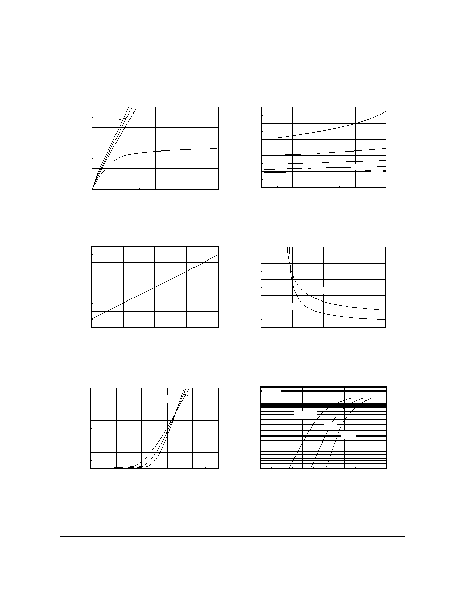
Figure 1. On-Region Characteristics.
Figure 2. On-Resistance Variation with
Drain Current and Gate Voltage.
0.6
0.8
1
1.2
1.4
1.6
-50
-25
0
25
50
75
100
125
150
T
J
, JUNCTION TEMPERATURE (
o
C)
R
DS(O
N)
, NORMALIZED
DRAIN-SOURCE ON-RESISTANCE
I
D
= 0.9A
V
GS
= 4.5V
0.1
0.2
0.3
0.4
0.5
0.6
1
2
3
4
5
V
GS
, GATE TO SOURCE VOLTAGE (V)
R
DS(O
N)
, ON-RESISTANCE (OHM)
I
D
= 0.5A
T
A
= 125
o
C
T
A
= 25
o
C
Figure 3. On-Resistance Variation with
Temperature.
Figure 4. On-Resistance Variation with
Gate-to-Source Voltage.
0
0.5
1
1.5
2
2.5
0.5
1
1.5
2
2.5
3
V
GS
, GATE TO SOURCE VOLTAGE (V)
I
D
, DRAIN CURRENT (A)
T
A
= -55
o
C
25
o
C
125
o
C
V
DS
= 5V
0.0001
0.001
0.01
0.1
1
10
0
0.2
0.4
0.6
0.8
1
1.2
V
SD
,
BODY DIODE FORWARD VOLTAGE (V)
I
S
,
REVERSE DRAI
N CURRENT (
A
)
V
GS
= 0V
T
A
= 125
o
C
25
o
C
-55
o
C
Figure 5. Transfer Characteristics.
Figure 6. Body Diode Forward Voltage Variation
with Source Current and Temperature.
FDV305N

FDV305N Rev D (W)
Typical Characteristics
0
1
2
3
4
5
0
0.5
1
1.5
Q
g
, GATE CHARGE (nC)
V
GS
,
GATE-
S
OURCE VOLTAGE (
V
)
I
D
= 0.9A
V
DS
= 5V
10V
15V
0
30
60
90
120
150
0
5
10
15
20
V
DS
, DRAIN TO SOURCE VOLTAGE (V)
CAPACI
TANCE (pF)
C
ISS
C
OSS
C
RSS
f = 1 MHz
V
GS
= 0 V
Figure 7. Gate Charge Characteristics.
Figure 8. Capacitance Characteristics.
0.01
0.1
1
10
0.1
1
10
100
V
DS
, DRAIN-SOURCE VOLTAGE (V)
I
D
, DRAIN CURRENT (A)
DC
1s
100ms
100
µs
R
DS(ON)
LIMIT
V
GS
= 4.5V
SINGLE PULSE
R
JA
= 357
o
C/W
T
A
= 25
o
C
10ms
1ms
0
1
2
3
4
5
0.001
0.01
0.1
1
10
100
1000
t
1
, TIME (sec)
P(pk), PEAK TRANSIENT POWER (W)
SINGLE PULSE
R
JA
= 357∞C/W
T
A
= 25∞C
Figure 9. Maximum Safe Operating Area.
Figure 10. Single Pulse Maximum
Power Dissipation.
0.001
0.01
0.1
1
0.0001
0.001
0.01
0.1
1
10
100
1000
t
1
, TIME (sec)
r(t), NORMALIZED EFFECTIVE TRANSIENT
THERM
A
L RESISTANCE
R
JA
(t) = r(t) * R
JA
R
JA
= 357
o
C/W
T
J
- T
A
= P * R
JA
(t)
Duty Cycle, D = t
1
/ t
2
P(pk)
t
1
t
2
SINGLE PULSE
0.01
0.02
0.05
0.1
0.2
D = 0.5
Figure 11. Transient Thermal Response Curve.
FDV305N

DISCLAIMER
FAIRCHILD SEMICONDUCTOR RESERVES THE RIGHT TO MAKE CHANGES WITHOUT FURTHER
NOTICE TO ANY PRODUCTS HEREIN TO IMPROVE RELIABILITY, FUNCTION OR DESIGN. FAIRCHILD
DOES NOT ASSUME ANY LIABILITY ARISING OUT OF THE APPLICATION OR USE OF ANY PRODUCT
OR CIRCUIT DESCRIBED HEREIN; NEITHER DOES IT CONVEY ANY LICENSE UNDER ITS PATENT
RIGHTS, NOR THE RIGHTS OF OTHERS.
TRADEMARKS
The following are registered and unregistered trademarks Fairchild Semiconductor owns or is authorized to use and is
not intended to be an exhaustive list of all such trademarks.
LIFE SUPPORT POLICY
FAIRCHILDS PRODUCTS ARE NOT AUTHORIZED FOR USE AS CRITICAL COMPONENTS IN LIFE SUPPORT
DEVICES OR SYSTEMS WITHOUT THE EXPRESS WRITTEN APPROVAL OF FAIRCHILD SEMICONDUCTOR CORPORATION.
As used herein:
1. Life support devices or systems are devices or
systems which, (a) are intended for surgical implant into
the body, or (b) support or sustain life, or (c) whose
failure to perform when properly used in accordance
with instructions for use provided in the labeling, can be
reasonably expected to result in significant injury to the
user.
2. A critical component is any component of a life
support device or system whose failure to perform can
be reasonably expected to cause the failure of the life
support device or system, or to affect its safety or
effectiveness.
PRODUCT STATUS DEFINITIONS
Definition of Terms
Datasheet Identification
Product Status
Definition
Advance Information
Preliminary
No Identification Needed
Obsolete
This datasheet contains the design specifications for
product development. Specifications may change in
any manner without notice.
This datasheet contains preliminary data, and
supplementary data will be published at a later date.
Fairchild Semiconductor reserves the right to make
changes at any time without notice in order to improve
design.
This datasheet contains final specifications. Fairchild
Semiconductor reserves the right to make changes at
any time without notice in order to improve design.
This datasheet contains specifications on a product
that has been discontinued by Fairchild semiconductor.
The datasheet is printed for reference information only.
Formative or
In Design
First Production
Full Production
Not In Production
ImpliedDisconnect
ISOPLANAR
LittleFET
MicroFET
MicroPak
MICROWIRE
MSX
MSXPro
OCX
OCXPro
OPTOLOGIC
‚
OPTOPLANAR
FACT
FACT Quiet Series
FAST
‚
FASTr
FRFET
GlobalOptoisolator
GTO
HiSeC
I
2
C
Rev. I2
ACEx
ActiveArray
Bottomless
CoolFET
CROSSVOLT
DOME
EcoSPARK
E
2
CMOS
TM
EnSigna
TM
PACMAN
POP
Power247
PowerTrench
‚
QFET
QS
QT Optoelectronics
Quiet Series
RapidConfigure
RapidConnect
SILENT SWITCHER
‚
SMART START
SPM
Stealth
SuperSOT-3
SuperSOT-6
SuperSOT-8
SyncFET
TinyLogic
‚
TruTranslation
UHC
UltraFET
‚
VCX
Across the board. Around the world.
The Power Franchise
Programmable Active Droop