 | ÐлекÑÑоннÑй компоненÑ: FDW2504P | СкаÑаÑÑ:  PDF PDF  ZIP ZIP |
Äîêóìåíòàöèÿ è îïèñàíèÿ www.docs.chipfind.ru
April 2000
PRELIMINARY
©
1999 Fairchild Semiconductor Corporation
FDW2504P Rev. C (W)
FDW2504P
Dual P-Channel 2.5V Specified PowerTrench
®
®
MOSFET
General Description
This P-Channel 2.5V specified MOSFET is a rugged
gate version of Fairchild Semiconductor's advanced
PowerTrench process. It has been optimized for power
management applications with a wide range of gate
drive voltage (2.5V 12V).
Applications
·
Load switch
·
Motor drive
·
DC/DC conversion
·
Power management
Features
·
3.8 A, 20 V, R
DS(ON)
= 0.043
@ V
GS
= 4.5 V
R
DS(ON)
= 0.070
@ V
GS
= 2.5V
·
Extended V
GSS
range (
±
12V) for battery applications
·
Low gate charge
·
High performance trench technology for extremely
low R
DS(ON)
·
Low profile TSSOP-8 package
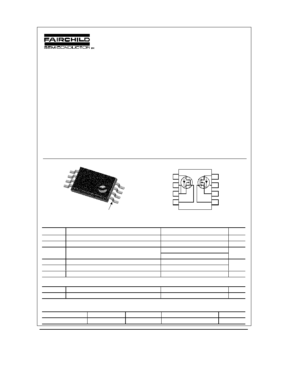
D1
S1
S1
G1
D2
S2
S2
G2
TSSOP-8
Pin 1
8
7
6
5
1
2
3
4
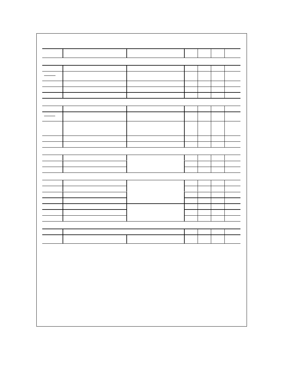
Absolute Maximum Ratings
T
A
=25
o
C unless otherwise noted
Symbol
Parameter
Ratings
Units
V
DSS
Drain-Source Voltage
-20
V
V
GSS
Gate-Source Voltage
±
12
V
I
D
Drain Current
Continuous
(Note 1a)
-3.8
A
Pulsed
-30
P
D
Power Dissipation
(Note 1a)
1.0
W
(Note 1b)
0.6
T
J
, T
STG
Operating and Storage Junction Temperature Range
-55 to +150
°
C
Thermal Characteristics
R
JA
Thermal Resistance, Junction-to-Ambient
(Note 1a)
125
°
C/W
(Note 1b)
208
Package Marking and Ordering Information
Device Marking
Device
Reel Size
Tape width
Quantity
2504P
FDW2504P
13''
12mm
3000 units
FDW2504P
FDW2504P Rev. C (W)
Electrical Characteristics
T
A
= 25°C unless otherwise noted
Symbol
Parameter
Test Conditions
Min Typ Max Units
Off Characteristics
BV
DSS
DrainSource Breakdown Voltage
V
GS
= 0 V, I
D
= 250
µ
A
20
V
BV
DSS
T
J
Breakdown Voltage Temperature
Coefficient
I
D
= 250
µ
A,Referenced to 25
°
C
16
mV/
°
C
I
DSS
Zero Gate Voltage Drain Current
V
DS
= 16 V,
V
GS
= 0 V
1
µ
A
I
GSSF
GateBody Leakage, Forward
V
GS
= 12 V,
V
DS
= 0 V
100
nA
I
GSSR
GateBody Leakage, Reverse
V
GS
= 12 V,
V
DS
= 0 V
100
nA
On Characteristics
(Note 2)
V
GS(th)
Gate Threshold Voltage
V
DS
= V
GS
, I
D
= 250
µ
A
0.6
1
1.5
V
V
GS(th)
T
J
Gate Threshold Voltage
Temperature Coefficient
I
D
= 250
µ
A,Referenced to 25
°
C
3
mV/
°
C
R
DS(on)
Static DrainSource
OnResistance
V
GS
= 4.5 V,
I
D
= 3.8 A
V
GS
= 2.5 V,
I
D
= 3.0 A
V
GS
=4.5 V, I
D
=3.8A, T
J
=125
°
C
0.036
0.056
0.049
0.043
0.070
0.069
I
D(on)
OnState Drain Current
V
GS
= 4.5 V,
V
DS
= 5 V
15
A
g
FS
Forward Transconductance
V
DS
= 5 V,
I
D
= 3.5 A
13.2
S
Dynamic Characteristics
C
iss
Input Capacitance
1015
pF
C
oss
Output Capacitance
446
pF
C
rss
Reverse Transfer Capacitance
V
DS
= 10 V,
V
GS
= 0 V,
f = 1.0 MHz
118
pF
Switching Characteristics
(Note 2)
t
d(on)
TurnOn Delay Time
11
20
ns
t
r
TurnOn Rise Time
18
32
ns
t
d(off)
TurnOff Delay Time
34
55
ns
t
f
TurnOff Fall Time
V
DD
= 5 V,
I
D
= 1 A,
V
GS
= 4.5 V,
R
GEN
= 6
34
55
ns
Q
g
Total Gate Charge
9.7
16
nC
Q
gs
GateSource Charge
2.2
nC
Q
gd
GateDrain Charge
V
DS
= 5 V,
I
D
= 3.8 A,
V
GS
= 4.5 V
2.4
nC
DrainSource Diode Characteristics and Maximum Ratings
I
S
Maximum Continuous DrainSource Diode Forward Current
0.83
A
V
SD
DrainSource Diode Forward
Voltage
V
GS
= 0 V,
I
S
= 0.83 A
(Note 2)
0.7
1.2
V
Notes:
1. R
JA
is the sum of the junction-to-case and case-to-ambient thermal resistance where the case thermal reference is defined as the solder mounting surface of
the drain pins. R
JC
is guaranteed by design while R
CA
is determined by the user's board design.
a) R
JA
is 125
°
C/W (steady state) when mounted on a 1 inch² copper pad on FR-4.
b) R
JA
is 208
°
C/W (steady state) when mounted on a minimum copper pad on FR-4.
2. Pulse Test: Pulse Width < 300
µ
s, Duty Cycle < 2.0%
FDW2504P
FDW2504P Rev. C (W)
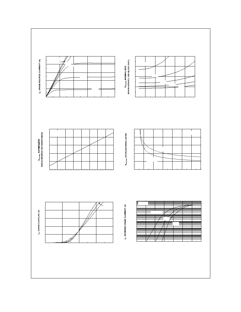
Typical Characteristics
0
6
12
18
24
30
0
1
2
3
4
5
-V
DS
, DRAIN-SOURCE VOLTAGE (V)
V
GS
= -4.5V
-2.5V
-3.5V
-3.0V
-2.0V
-4.0V
0.8
1
1.2
1.4
1.6
0
5
10
15
20
25
30
- I
D
, DRAIN CURRENT (A)
V
GS
= -2.5V
-3.5V
-4.5V
-3.0V
-4.0V
Figure 1. On-Region Characteristics.
Figure 2. On-Resistance Variation with
Drain Current and Gate Voltage.
0.6
0.8
1
1.2
1.4
1.6
-50
-25
0
25
50
75
100
125
150
T
J
, JUNCTION TEMPERATURE (
o
C)
I
D
= -3.8A
V
GS
= -4.5V
0
0.03
0.06
0.09
0.12
0.15
1.5
2
2.5
3
3.5
4
4.5
5
-V
GS
, GATE TO SOURCE VOLTAGE (V)
I
D
= -1.9A
T
A
= 125
o
C
T
A
= 25
o
C
Figure 3. On-Resistance Variation
withTemperature.
Figure 4. On-Resistance Variation with
Gate-to-Source Voltage.
0
6
12
18
24
30
0.4
1.3
2.2
3.1
4
-V
GS
, GATE TO SOURCE VOLTAGE (V)
T
A
= -55
o
C
25
o
C
125
o
C
V
DS
= -5V
0.0001
0.001
0.01
0.1
1
10
100
0
0.2
0.4
0.6
0.8
1
1.2
1.4
-V
SD
, BODY DIODE FORWARD VOLTAGE (V)
T
A
= 125
o
C
25
o
C
-55
o
C
V
GS
= 0V
Figure 5. Transfer Characteristics.
Figure 6. Body Diode Forward Voltage Variation
with Source Current and Temperature.
FDW2504P
FDW2504P Rev. C (W)
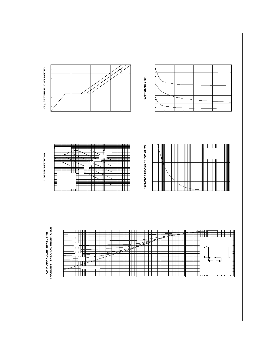
Typical Characteristics
0
1
2
3
4
5
0
3
6
9
12
Q
g
, GATE CHARGE (nC)
I
D
= -3.8A
V
DS
= -5V
-10V
-15V
0
300
600
900
1200
1500
1800
0
5
10
15
20
-V
DS
, DRAIN TO SOURCE VOLTAGE (V)
C
ISS
C
RSS
C
OSS
f = 1MHz
V
GS
= 0 V
Figure 7. Gate Charge Characteristics.
Figure 8. Capacitance Characteristics.
0.01
0.1
1
10
100
0.1
1
10
100
V
DS
, DRAIN-SOURCE VOLTAGE (V)
DC
10s
1s
100ms
R
DS(ON)
LIMIT
V
GS
= 4.5V
SINGLE PULSE
R
JA
= 208
o
C/W
T
A
= 25
o
C
10ms
1ms
0
10
20
30
40
50
0.001
0.01
0.1
1
10
100
1000
t
1
, TIME (sec)
SINGLE PULSE
R
JA
= 208°C/W
T
A
= 25°C
Figure 9. Maximum Safe Operating Area.
Figure 10. Single Pulse Maximum
Power Dissipation.
0.001
0.01
0.1
1
0.0001
0.001
0.01
0.1
1
10
100
1000
t
1
, TIME (sec)
R
JA
(t) = r(t) + R
JA
R
JA
=208 °C/W
T
J
- T
A
= P * R
JA
(t)
Duty Cycle, D = t
1
/ t
2
P(pk)
t
1
t
2
SINGLE PULSE
0.01
0.02
0.05
0.1
0.2
D = 0.5
Figure 11. Transient Thermal Response Curve.
Thermal characterization performed using the conditions described in Note 1b.
Transient thermal response will change depending on the circuit board design.
FDW2504P
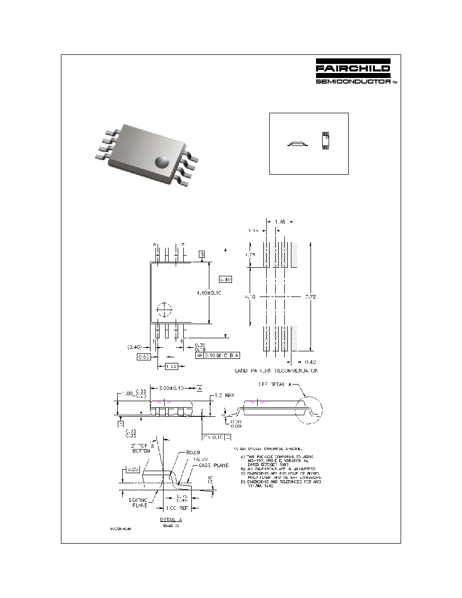
TSSOP-8 (FS PKG Code S4)
TSSOP-8 Package Dimensions
January 2000, Rev. B
1:1
Scale 1:1 on letter size paper
Dimensions shown below are in millimeters
Part Weight per unit (gram): 0.0334

TRADEMARKS
ACExTM
BottomlessTM
CoolFETTM
CROSSVOLTTM
E
2
CMOS
TM
FACTTM
FACT Quiet SeriesTM
FAST
FASTrTM
GTOTM
The following are registered and unregistered trademarks Fairchild Semiconductor owns or is authorized to use and is
not intended to be an exhaustive list of all such trademarks.
LIFE SUPPORT POLICY
FAIRCHILD'S PRODUCTS ARE NOT AUTHORIZED FOR USE AS CRITICAL COMPONENTS IN LIFE SUPPORT
DEVICES OR SYSTEMS WITHOUT THE EXPRESS WRITTEN APPROVAL OF FAIRCHILD SEMICONDUCTOR CORPORATION.
As used herein:
1. Life support devices or systems are devices or
systems which, (a) are intended for surgical implant into
the body, or (b) support or sustain life, or (c) whose
failure to perform when properly used in accordance
with instructions for use provided in the labeling, can be
reasonably expected to result in significant injury to the
user.
2. A critical component is any component of a life
support device or system whose failure to perform can
be reasonably expected to cause the failure of the life
support device or system, or to affect its safety or
effectiveness.
PRODUCT STATUS DEFINITIONS
Definition of Terms
Datasheet Identification
Product Status
Definition
Advance Information
Preliminary
No Identification Needed
Obsolete
This datasheet contains the design specifications for
product development. Specifications may change in
any manner without notice.
This datasheet contains preliminary data, and
supplementary data will be published at a later date.
Fairchild Semiconductor reserves the right to make
changes at any time without notice in order to improve
design.
This datasheet contains final specifications. Fairchild
Semiconductor reserves the right to make changes at
any time without notice in order to improve design.
This datasheet contains specifications on a product
that has been discontinued by Fairchild semiconductor.
The datasheet is printed for reference information only.
Formative or
In Design
First Production
Full Production
Not In Production
DISCLAIMER
FAIRCHILD SEMICONDUCTOR RESERVES THE RIGHT TO MAKE CHANGES WITHOUT FURTHER
NOTICE TO ANY PRODUCTS HEREIN TO IMPROVE RELIABILITY, FUNCTION OR DESIGN. FAIRCHILD
DOES NOT ASSUME ANY LIABILITY ARISING OUT OF THE APPLICATION OR USE OF ANY PRODUCT
OR CIRCUIT DESCRIBED HEREIN; NEITHER DOES IT CONVEY ANY LICENSE UNDER ITS PATENT
RIGHTS, NOR THE RIGHTS OF OTHERS.
SuperSOTTM-8
SyncFETTM
TinyLogicTM
UHCTM
VCXTM
HiSeCTM
ISOPLANARTM
MICROWIRETM
POPTM
PowerTrench
QFETTM
QSTM
Quiet SeriesTM
SuperSOTTM-3
SuperSOTTM-6
Rev. E