 | ÐлекÑÑоннÑй компоненÑ: FDW2512NZ | СкаÑаÑÑ:  PDF PDF  ZIP ZIP |
Äîêóìåíòàöèÿ è îïèñàíèÿ www.docs.chipfind.ru
©2004 Fairchild Semiconductor Corporation
FDW2512NZ Rev. A
December 2004
www.fairchildsemi.com
FDW2512NZ D
u
al
N-Channel 2.
5V Speci
fie
d
Power
T
re
n
c
h® MOSFET
1
FDW2512NZ
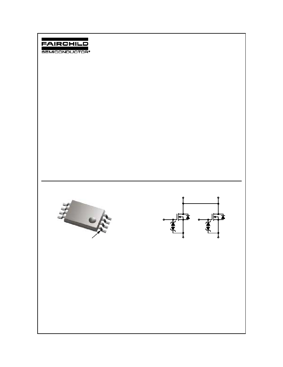
Dual N-Channel 2.5V Specified PowerTrench
®
MOSFET
Features
!
6A, 20V r
DS(ON)
= 0.028
,
V
GS
= 4.5V
r
DS(ON)
= 0.036
,
V
GS
= 2.5V
!
Extended V
GS
range (
±
12 V) for battery applications
!
HBM ESD Protection Level of 3.5kV Typical (note 3)
!
High performance trench technology for extremely low
r
DS(ON)
!
Low profile TSSOP-8 package
Applications
!
Load switch
!
Battery charge
!
Battery disconnect circuits
General Description
This N-Channel MOSFET is produced using Fairchild
Semiconductor's advanced PowerTrench process that has
been especially tailored to minimize the on-state resistance
and yet maintain low gate charge for superior switching
performance. These devices are well suited for portable
electronics applications.
TSSOP-8
D1
G1
S1
D2
G2
S2
S2
G2
D2
S2
G1
S1
S1
D1
Pin 1
FDW2512NZ Rev. A
FDW2512NZ D
u
al
N-Channel 2.
5V Speci
fie
d
Power
T
re
n
c
h® MOSFET
FDW2512NZ D
u
al
N-Channel 2.
5V Speci
fie
d
Power
T
re
n
c
h® MOSFET
www.fairchildsemi.com
2
Absolute Maximum Ratings
T
A
=25°C unless otherwise noted
Thermal Characteristics
Package Marking and Ordering Information
Electrical Characteristics
T
A
= 25°C unless otherwise noted
Off Characteristics
On Characteristics
Dynamic Characteristics
Symbol
Parameter
Ratings
Units
V
DSS
Drain to Source Voltage
20
V
V
GS
Gate to Source Voltage
±
12
V
I
D
Drain Current
Continuous (T
C
= 25
o
C, V
GS
= 4.5V, R
JA
= 77
o
C/W)
6.0
A
Continuous
(T
C
= 100
o
C, V
GS
= 2.5V, R
JA
= 77
o
C/W) 3.3
A
Pulsed
Figure 4
A
P
D
Power dissipation
1.6
W
Derate above 25°C
13
mW/
o
C
T
J
, T
STG
Operating and Storage Temperature
-55 to 150
o
C
R
JA
Thermal Resistance Junction to Ambient (Note 1)
77
o
C/W
R
JA
Thermal Resistance Junction to Ambient (Note 2)
114
o
C/W
Device Marking
Device
Package
Reel Size
Tape Width
Quantity
2512NZ
FDW2512NZ
TSSOP-8
13"
12 mm
2500 units
2512NZ
FDW2512NZ_NL (Note 4)
TSSOP-8
13"
12 mm
2500 units
Symbol
Parameter
Test Conditions
Min
Typ
Max
Units
B
VDSS
Drain to Source Breakdown Voltage
I
D
= 250
µ
A, V
GS
= 0V
20
-
-
V
I
DSS
Zero Gate Voltage Drain Current
V
DS
= 16V
-
-
1
µ
A
V
GS
= 0V
T
A
= 100
o
C
-
-
5
I
GSS
Gate to Source Leakage Current
V
GS
=
±
12V -
-
±
10
µ
A
V
GS
=
±
4.5V
±
250
nA
V
GS(TH)
Gate to Source Threshold Voltage
V
GS
= V
DS
, I
D
= 250
µ
A
0.6
0.8
1.5
V
r
DS(ON)
Drain to Source On Resistance
I
D
= 6.0A, V
GS
= 4.5V
-
0.017
0.028
I
D
= 5.9A, V
GS
= 4.0V
-
0.018
0.029
I
D
= 5.3A, V
GS
= 3.1V
-
0.019
0.035
I
D
= 5.3A, V
GS
= 2.5V
-
0.022
0.036
C
ISS
Input Capacitance
V
DS
= 10V, V
GS
= 0V,
f = 1MHz
-
670
-
pF
C
OSS
Output Capacitance
-
170
-
pF
C
RSS
Reverse Transfer Capacitance
-
115
-
pF
R
G
Gate Resistance
V
GS
= 0.5V, f = 1MHz
-
4.2
-
Q
g(TOT)
Total Gate Charge at 4.5V
V
GS
= 0V to 4.5V
V
DD
= 10V
I
D
= 6.0A
I
g
= 1.0mA
-
8
12
nC
Q
g(2.5)
Total Gate Charge at 2.5V
V
GS
= 0V to 2.5V
-
5.1
7.6
nC
Q
gs
Gate to Source Gate Charge
-
1.1
-
nC
Q
gd
Gate to Drain "Miller" Charge
-
2.2
-
nC
FDW2512NZ Rev. A
FDW2512NZ D
u
al
N-Channel 2.
5V Speci
fie
d
Power
T
re
n
c
h® MOSFET
FDW2512NZ D
u
al
N-Channel 2.
5V Speci
fie
d
Power
T
re
n
c
h® MOSFET
www.fairchildsemi.com
3
Switching Characteristics
(V
GS
= 4.5V)
Drain-Source Diode Characteristics
Notes:
1. R
JA
is 77
o
C/W (steady state) when mounted on a 1 inch
2
copper pad on FR-4
.
2. R
JA
is 114
o
C/W (steady state) when mounted on a mininum copper pad on FR-4.
3. The diode connected to the gate and source serves only as protection against ESD. No gate overvoltage rating is implied.
4. FDW2512NZ_NL is lead free product. FDW2512NZ_NL marking will appear on the reel label.
t
ON
Turn-On Time
V
DD
= 10V, I
D
= 6.0A
V
GS
= 4.5V, R
GS
= 16
-
-
98
ns
t
d(ON)
Turn-On Delay Time
-
8
-
ns
t
r
Rise Time
-
57
-
ns
t
d(OFF)
Turn-Off Delay Time
-
47
-
ns
t
f
Fall Time
-
58
-
ns
t
OFF
Turn-Off Time
-
-
158
ns
V
SD
Source to Drain Diode Voltage
I
SD
= 1.3A
-
0.7
1.2
V
t
rr
Reverse Recovery Time
I
SD
= 6.0A, dI
SD
/dt = 100A/
µ
s
-
-
24
ns
Q
RR
Reverse Recovered Charge
I
SD
= 6.0A, dI
SD
/dt = 100A/
µ
s
-
-
13
nC
FDW2512NZ Rev. A
FDW2512NZ D
u
al
N-Channel 2.
5V Speci
fie
d
Power
T
re
n
c
h® MOSFET
FDW2512NZ D
u
al
N-Channel 2.
5V Speci
fie
d
Power
T
re
n
c
h® MOSFET
www.fairchildsemi.com
4
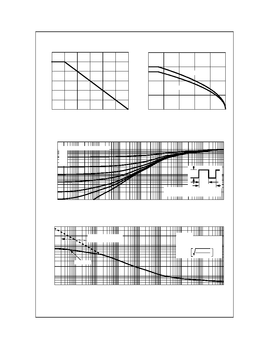
Typical Characteristic
T
A
= 25°C unless otherwise noted
Figure 1. Normalized Power Dissipation vs
Ambient Temperature
Figure 2. Maximum Continuous Drain Current vs
Ambient Temperature
Figure 3. Normalized Maximum Transient Thermal Impedance
Figure 4. Peak Current Capability
T
A
, AMBIENT TEMPERATURE (
o
C)
P
O
W
E
R DIS
S
I
P
A
T
ION M
U
L
T
IP
L
I
E
R
0
0
25
50
75
100
150
0.2
0.4
0.6
0.8
1.0
1.2
125
0
2
4
6
8
25
50
75
100
125
150
ID
,
D
RAIN CURRENT
(
A
)
T
A
, AMBIENT TEMPERATURE (
o
C)
V
GS
= 4.5V
V
GS
= 2.5V
0.01
0.1
1
10
-5
10
-4
10
-3
10
-2
10
-1
10
0
10
1
10
2
10
3
2
t, RECTANGULAR PULSE DURATION (s)
Z
JA
,
NORM
AL
IZ
ED
T
H
ERM
A
L
I
M
PE
D
ANCE
NOTES:
DUTY FACTOR: D = t
1
/t
2
PEAK T
J
= P
DM
x Z
JA
x R
JA
+ T
A
P
DM
t
1
t
2
0.5
0.2
0.1
0.05
0.01
0.02
DUTY CYCLE - DESCENDING ORDER
10
100
10
-5
10
-4
10
-3
10
-2
10
-1
10
0
10
1
10
2
10
3
400
5
I
DM
, PE
AK CURREN
T
(
A
)
t, PULSE WIDTH (s)
TRANSCONDUCTANCE
MAY LIMIT CURRENT
IN THIS REGION
V
GS
= 2.5V
T
A
= 25
o
C
I = I
25
150 - T
A
125
FOR TEMPERATURES
ABOVE 25
o
C DERATE PEAK
CURRENT AS FOLLOWS:
FDW2512NZ Rev. A
FDW2512NZ D
u
al
N-Channel 2.
5V Speci
fie
d
Power
T
re
n
c
h® MOSFET
FDW2512NZ D
u
al
N-Channel 2.
5V Speci
fie
d
Power
T
re
n
c
h® MOSFET
www.fairchildsemi.com
5
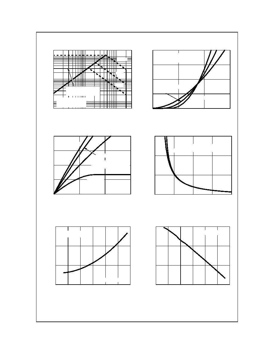
Figure 5. Forward Bias Safe Operating Area
Figure 6. Transfer Characteristics
Figure 7. Saturation Characteristics
Figure 8. Drain to Source On Resistance vs Gate
Voltage and Drain Current
Figure 9. Normalized Drain to Source On
Resistance vs Junction Temperature
Figure 10. Normalized Gate Threshold Voltage vs
Junction Temperature
Typical Characteristic
(Continued) T
A
= 25°C unless otherwise noted
1
10
100
0.1
1
10
30
400
0.5
V
DS
, DRAIN TO SOURCE VOLTAGE (V)
I
D
,
D
RAIN CURRENT
(
A
)
T
J
= MAX RATED
T
A
= 25
o
C
SINGLE PULSE
LIMITED BY r
DS(ON)
AREA MAY BE
OPERATION IN THIS
100
µ
s
10ms
1ms
0
10
20
30
40
1.0
1.5
2.0
2.5
I
D
, DRAIN CURRE
NT
(
A
)
V
GS
, GATE TO SOURCE VOLTAGE (V)
PULSE DURATION = 80
µ
s
DUTY CYCLE = 0.5% MAX
V
DD
= 10V
T
J
= 150
o
C
T
J
= 25
o
C
T
J
= -55
o
C
0
10
20
30
40
0
0.5
1.0
1.5
I
D
, DRAIN CURRE
NT
(
A
)
V
DS
, DRAIN TO SOURCE VOLTAGE (V)
V
GS
= 2.5V
PULSE DURATION = 80
µ
s
DUTY CYCLE = 0.5% MAX
V
GS
= 1.8V
T
A
= 25
o
C
V
GS
= 4.5V
V
GS
= 10V
30
45
60
1
2
3
4
5
15
I
D
= 1A
V
GS
, GATE TO SOURCE VOLTAGE (V)
I
D
= 6A
r
DS(
O
N)
, DRAIN T
O
SOURCE
O
N
R
ESI
ST
A
NCE
(
m
)
PULSE DURATION = 80
µ
s
DUTY CYCLE = 0.5% MAX
0.75
1.00
1.25
1.50
-80
-40
0
40
80
120
160
NORM
AL
IZ
ED DRAIN T
O
SOURCE
T
J
, JUNCTION TEMPERATURE (
o
C)
O
N
R
ESI
ST
A
NCE
V
GS
= 4.5V, I
D
= 6A
PULSE DURATION = 80
µ
s
DUTY CYCLE = 0.5% MAX
0.50
0.75
1.00
1.25
-80
-40
0
40
80
120
160
NORM
AL
IZ
E
D
GA
T
E
T
J
, JUNCTION TEMPERATURE (
o
C)
V
GS
= V
DS
, I
D
= 250
µ
A
T
HRES
H
OL
D V
O
L
T
A
G
E