 | ÐлекÑÑоннÑй компоненÑ: FDW252P | СкаÑаÑÑ:  PDF PDF  ZIP ZIP |
Äîêóìåíòàöèÿ è îïèñàíèÿ www.docs.chipfind.ru
June 2000
PRELIMINARY
2000 Fairchild Semiconductor Corporation
FDW252P Rev. B(W)
FDW252P
P-Channel 2.5V Specified PowerTrench
MOSFET
General Description
This P-Channel 2.5V specified MOSFET is a rugged
gate version of Fairchild Semiconductor's advanced
PowerTrench process. It has been optimized for power
management applications with a wide range of gate
drive voltage (2.5V 12V).
Applications
· Load
switch
· Motor
drive
· DC/DC
conversion
· Power
management
Features
·
8.8 A, 20 V. R
DS(ON)
= 0.012
@ V
GS
= 4.5 V
R
DS(ON)
= 0.018
@ V
GS
= 2.5 V
· Extended
V
GSS
range (
±12V) for battery
applications
·
Low gate charge
·
High performance trench technology for extremely
low R
DS(ON)
·
Low profile TSSOP-8 package
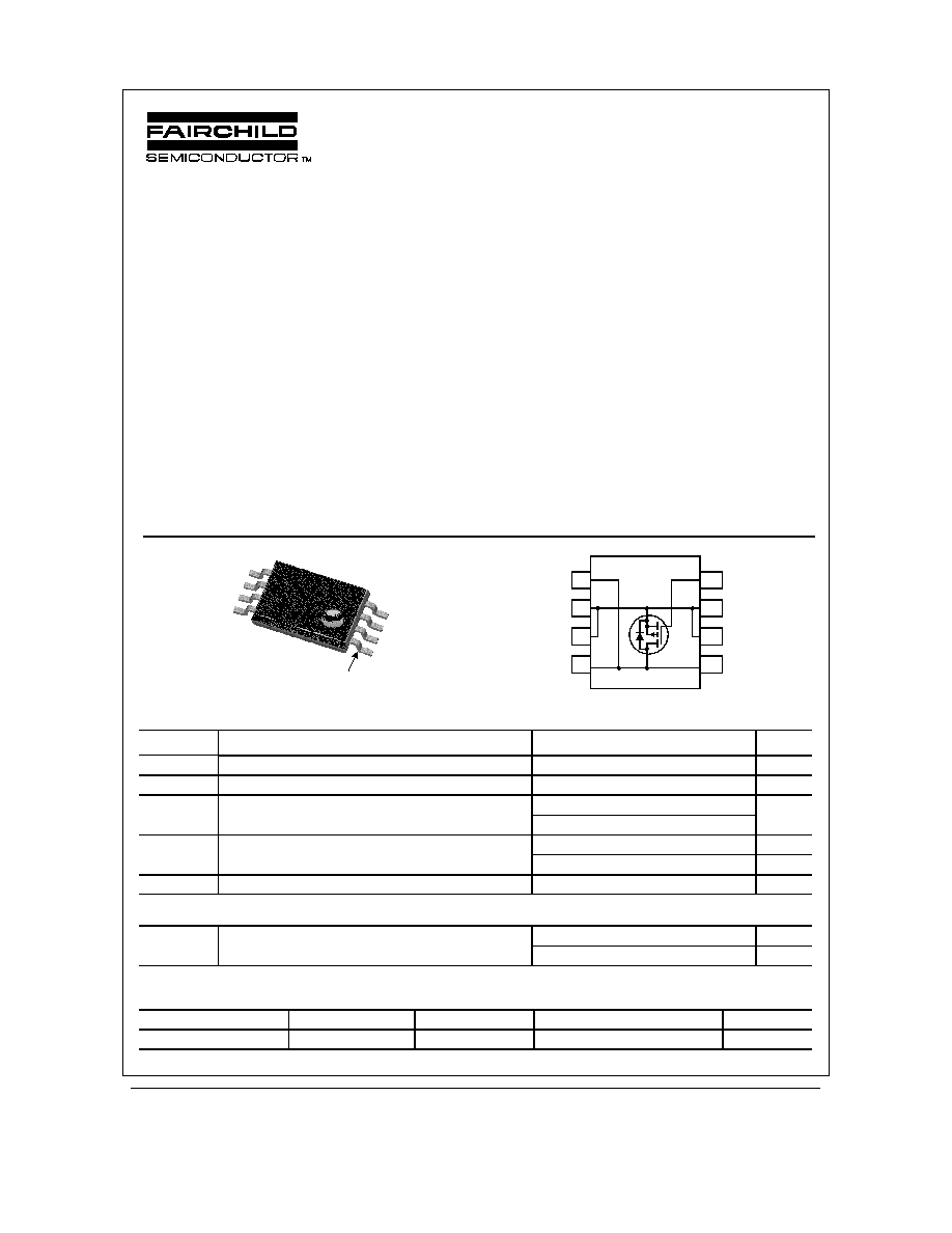
D
S
S
G
D
S
S
D
TSSOP-8
Pin 1
4
3
2
1
5
6
7
8
Absolute Maximum Ratings
T
A
=25
o
C unless otherwise noted
Symbol
Parameter
Ratings
Units
V
DSS
Drain-Source Voltage
-20
V
V
GSS
Gate-Source Voltage
± 12
V
I
D
Drain Current Continuous
(Note 1)
-8.8
A
Pulsed
-50
P
D
Power Dissipation
(Note 1a)
1.3
W
(Note 1b)
0.6
T
J
, T
STG
Operating and Storage Junction Temperature Range
-55 to +150
°C
Thermal Characteristics
R
JA
Thermal Resistance, Junction-to-Ambient
(Note 1a)
96
°C/W
(Note 1b)
208
Package Marking and Ordering Information
Device Marking
Device
Reel Size
Tape width
Quantity
252P
FDW252P
13''
16mm
3000 units
FDW252P
FDW252P Rev. B(W)
Electrical Characteristics
T
A
= 25°C unless otherwise noted
Symbol
Parameter
Test Conditions
Min Typ Max Units
Off Characteristics
BV
DSS
DrainSource Breakdown Voltage V
GS
= 0 V, I
D
= 250
µA
20
V
BV
DSS
===T
J
Breakdown Voltage Temperature
Coefficient
I
D
= 250
µA, Referenced to 25°C
12
mV/
°C
I
DSS
Zero Gate Voltage Drain Current
V
DS
= 16 V,
V
GS
= 0 V
1
µA
I
GSSF
GateBody Leakage, Forward
V
GS
= 12 V,
V
DS
= 0 V
100
nA
I
GSSR
GateBody Leakage, Reverse
V
GS
= 12 V,
V
DS
= 0 V
100
nA
On Characteristics
(Note 2)
V
GS(th)
Gate Threshold Voltage
V
DS
= V
GS
, I
D
= 250
µA
0.6
0.8
1.5
V
V
GS(th)
===T
J
Gate Threshold Voltage
Temperature Coefficient
I
D
= 250
µA, Referenced to 25°C
3.5
mV/
°C
R
DS(on)
Static DrainSource
OnResistance
V
GS
= 4.5 V,
I
D
= 8.8 A
V
GS
= 2.5 V,
I
D
= 7.2 A
V
GS
= 4.5 V, I
D
= 8.8 A, T
J
= 125
°C
9
13
13
12
18
20
m
I
D(on)
OnState Drain Current
V
GS
= 4.5 V,
V
DS
= 5 V
50
A
g
FS
Forward Transconductance
V
DS
= 10 V,
I
D
= 8.8 A
46
S
Dynamic Characteristics
C
iss
Input Capacitance
5045
pF
C
oss
Output Capacitance
1035
pF
C
rss
Reverse Transfer Capacitance
V
DS
= 10 V,
V
GS
= 0 V,
f = 1.0 MHz
549
pF
Switching Characteristics
(Note 2)
t
d(on)
TurnOn Delay Time
8
16
ns
t
r
TurnOn Rise Time
14
25
ns
t
d(off)
TurnOff Delay Time
130
208
ns
t
f
TurnOff Fall Time
V
DD
= 10 V,
I
D
= 1 A,
V
GS
= 4.5 V,
R
GEN
= 6
80
128
ns
Q
g
Total Gate Charge
41
66
nC
Q
gs
GateSource Charge
7
nC
Q
gd
GateDrain Charge
V
DS
= 10 V,
I
D
= 8.8 A,
V
GS
= 4.5 V
11
nC
DrainSource Diode Characteristics and Maximum Ratings
I
S
Maximum Continuous DrainSource Diode Forward Current
1.2
A
V
SD
DrainSource Diode Forward
Voltage
V
GS
= 0 V,
I
S
= 1.2 A
(Note 2)
0.6
1.2
V
Notes:
1. R
JA
is the sum of the junction-to-case and case-to-ambient thermal resistance where the case thermal reference is defined as the solder mounting surface
of the drain pins. R
JC
is guaranteed by design while R
CA
is determined by the user's board design.
a) R
JA
is 96
°C/W (steady state) when mounted on a 1 inch² copper pad on FR-4.
b) R
JA
is 208
°C/W (steady state) when mounted on a minimum copper pad on FR-4.
2. Pulse Test: Pulse Width < 300
µs, Duty Cycle < 2.0%
FDW252P
FDW252P Rev. B(W)
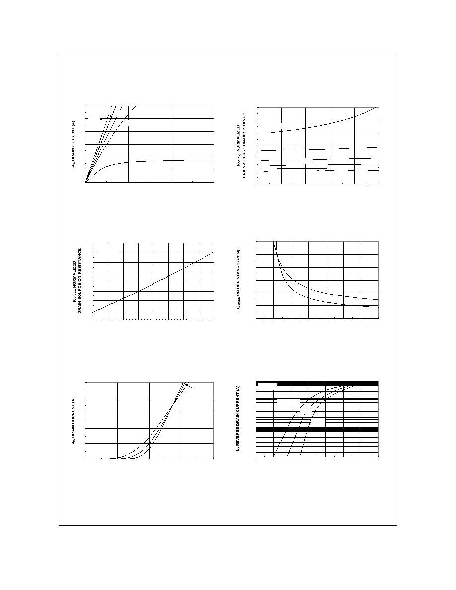
Typical Characteristics
0
5
10
15
20
25
30
0
0.5
1
1.5
-V
DS
, DRAIN TO SOURCE VOLTAGE (V)
V
GS
= -4.5V
-2.5V
-2.0V
-1.5V
-3.0V
0.8
1
1.2
1.4
1.6
1.8
2
0
6
12
18
24
30
-I
D
, DIRAIN CURRENT (A)
V
GS
= -2.0V
-3.0V
-3.5V
-4.0V
-4.5V
-2.5V
Figure 1. On-Region Characteristics.
Figure 2. On-Resistance Variation with
Drain Current and Gate Voltage.
0.7
0.8
0.9
1
1.1
1.2
1.3
1.4
1.5
-50
-25
0
25
50
75
100
125
150
T
J
, JUNCTION TEMPERATURE (
o
C)
I
D
= -8.8A
V
GS
= -4.5V
0.005
0.01
0.015
0.02
0.025
0.03
0.035
1.5
2
2.5
3
3.5
4
4.5
5
-V
GS
, GATE TO SOURCE VOLTAGE (V)
I
D
= -4.4A
T
A
= 125
o
C
T
A
= 25
o
C
Figure 3. On-Resistance Variation
withTemperature.
Figure 4. On-Resistance Variation with
Gate-to-Source Voltage.
0
10
20
30
40
50
0.5
1
1.5
2
2.5
-V
GS
, GATE TO SOURCE VOLTAGE (V)
T
A
= -55
o
C
25
o
C
125
o
C
V
DS
= -5V
0.001
0.01
0.1
1
10
100
0
0.2
0.4
0.6
0.8
1
1.2
1.4
-V
SD
,
BODY DIODE FORWARD VOLTAGE (V)
V
GS
= 0V
T
A
= 125
o
C
25
o
C
-55
o
C
Figure 5. Transfer Characteristics.
Figure 6. Body Diode Forward Voltage Variation
with Source Current and Temperature.
FDW252P
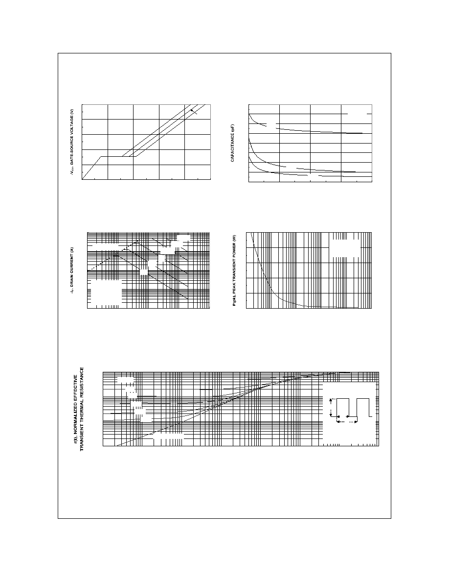
FDW252P Rev. B(W)
Typical Characteristics
0
1
2
3
4
5
0
10
20
30
40
50
Q
g
, GATE CHARGE (nC)
I
D
= -8.8A
V
DS
= -5V
-10V
-15V
0
1000
2000
3000
4000
5000
6000
7000
8000
0
3
6
9
12
-V
DS
, DRAIN TO SOURCE VOLTAGE (V)
C
ISS
C
OSS
C
RSS
f = 1 MHz
V
GS
= 0 V
Figure 7. Gate Charge Characteristics.
Figure 8. Capacitance Characteristics.
0.01
0.1
1
10
100
0.01
0.1
1
10
100
-V
DS
, DRAIN-SOURCE VOLTAGE (V)
DC
10s
1s
100ms
100µs
R
DS(ON)
LIMIT
V
GS
= -4.5V
SINGLE PULSE
R
JA
= 208
o
C/W
T
A
= 25
o
C
10ms
0
10
20
30
40
50
0.01
0.1
1
10
100
1000
t
1
, TIME (sec)
SINGLE PULSE
R
JA
= 208°C/W
T
A
= 25°C
Figure 9. Maximum Safe Operating Area.
Figure 10. Single Pulse Maximum
Power Dissipation.
0.001
0.01
0.1
1
0.0001
0.001
0.01
0.1
1
10
100
1000
t
1
, TIME (sec)
R
JA
(t) = r(t) + R
JA
R
JA
= 208 °C/W
T
J
- T
A
= P * R
JA
(t)
Duty Cycle, D = t
1
/ t
2
P(pk)
t
1
t
2
SINGLE PULSE
0.01
0.02
0.05
0.1
0.2
D = 0.5
Figure 11. Transient Thermal Response Curve.
Thermal characterization performed using the conditions described in Note 1b.
Transient thermal response will change depending on the circuit board design.
FDW252P
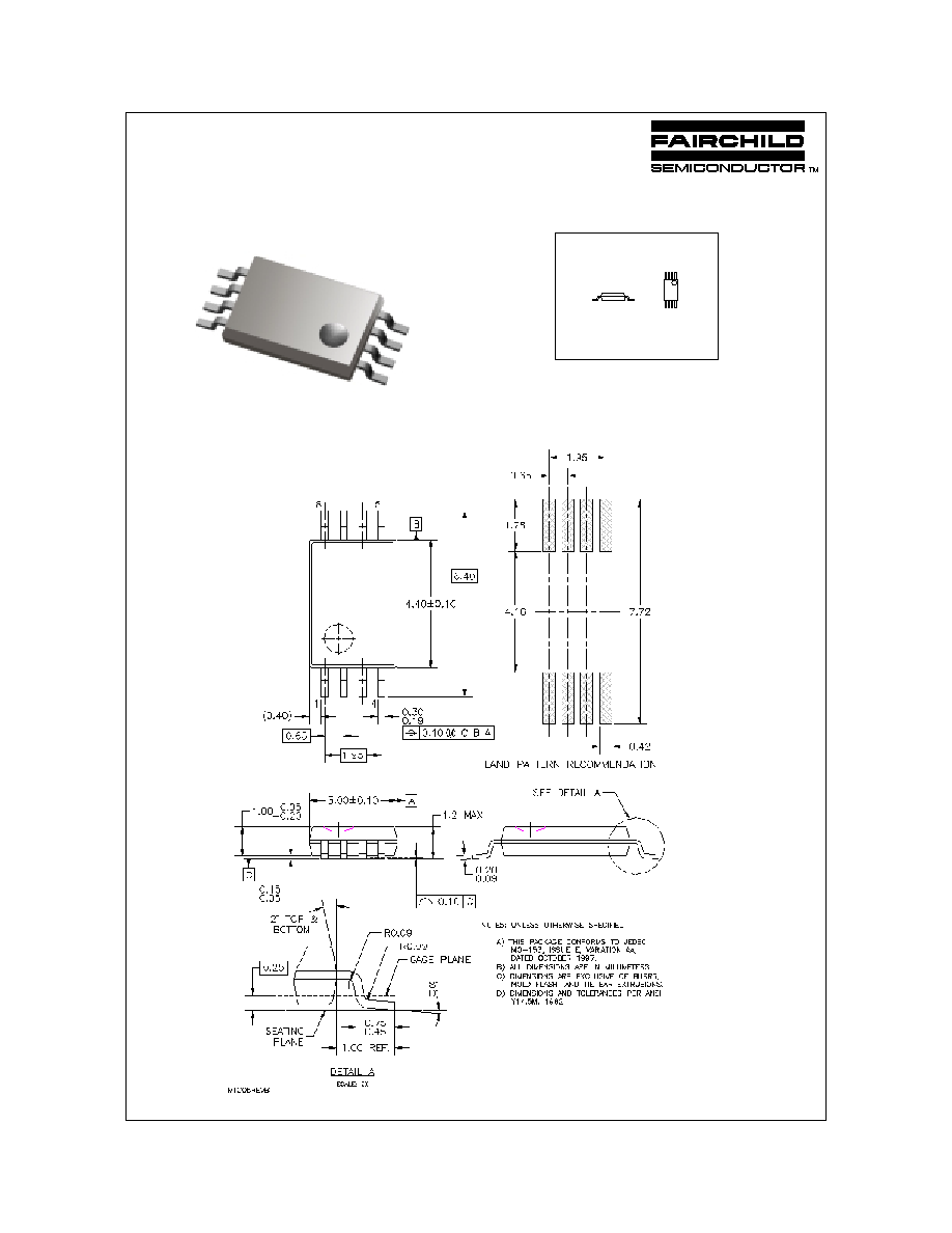
TSSOP-8 (FS PKG Code S4)
TSSOP-8 Package Dimensions
January 2000, Rev. B
1:1
Scale 1:1 on letter size paper
Dimensions shown below are in millimeters
Part Weight per unit (gram): 0.0334