
©2004 Fairchild Semiconductor Corporation
FDW2601NZ Rev. A
December 2004
www.fairchildsemi.com
FDW2601NZ D
u
al
N-Channel 2.
5V Speci
fie
d
Power
T
re
n
c
hÆ MOSFET
1
FDW2601NZ
Dual N-Channel 2.5V Specified PowerTrench
Æ
MOSFET
Features
!
8.2A, 30V r
DS(ON)
= 0.015
,
V
GS
= 4.5V
r
DS(ON)
= 0.020
,
V
GS
= 2.5V
!
Extended V
GS
range (
±
12 V) for battery applications
!
HBM ESD Protection Level of 3.5kV Typical (note 3)
!
High performance trench technology for extremely low
r
DS(ON)
!
Low profile TSSOP-8 package
Applications
!
Load switch
!
Battery charge
!
Battery disconnect circuits
General Description
This N-Channel MOSFET is produced using Fairchild
Semiconductor's advanced PowerTrench process that has
been especially tailored to minimize the on-state resistance
and yet maintain low gate charge for superior switching
performance. These devices are well suited for portable
electronics applications.
TSSOP-8
D1
G1
S1
D2
G2
S2
S2
G2
D2
S2
G1
S1
S1
D1
Pin 1

FDW2601NZ Rev. A
www.fairchildsemi.com
FDW2601NZ D
u
al
N-Channel 2.
5V Speci
fie
d
Power
T
re
n
c
hÆ MOSFET
2
Absolute Maximum Ratings
T
A
=25∞C unless otherwise noted
Thermal Characteristics
Package Marking and Ordering Information
Electrical Characteristics
T
A
= 25∞C unless otherwise noted
Off Characteristics
On Characteristics
Dynamic Characteristics
Symbol
Parameter
Ratings
Units
V
DSS
Drain to Source Voltage
30
V
V
GS
Gate to Source Voltage
±
12
V
I
D
Drain Current
Continuous (T
C
= 25
o
C, V
GS
= 4.5V, R
JA
= 77
o
C/W)
8.2
A
Continuous
(T
C
= 100
o
C, V
GS
= 2.5V, R
JA
= 77
o
C/W) 4.5
A
Pulsed
Figure 4
A
P
D
Power dissipation
1.6
W
Derate above 25∞C
13
mW/
o
C
T
J
, T
STG
Operating and Storage Temperature
-55 to 150
o
C
R
JA
Thermal Resistance Junction to Ambient (Note 1)
77
o
C/W
R
JA
Thermal Resistance Junction to Ambient (Note 2)
114
o
C/W
Device Marking
Device
Package
Reel Size
Tape Width
Quantity
2601NZ
FDW2601NZ
TSSOP-8
13"
12 mm
2500 units
2601NZ
FDW2601NZ_NL (Note 4)
TSSOP-8
13"
12 mm
2500 units
Symbol
Parameter
Test Conditions
Min
Typ
Max
Units
B
VDSS
Drain to Source Breakdown Voltage
I
D
= 250
µ
A, V
GS
= 0V
30
-
-
V
I
DSS
Zero Gate Voltage Drain Current
V
DS
= 24V
-
-
1
µ
A
V
GS
= 0V
T
A
= 100
o
C
-
-
5
I
GSS
Gate to Source Leakage Current
V
GS
=
±
12V -
-
±
10
µ
A
V
GS
=
±
4.5V
±
250
nA
V
GS(TH)
Gate to Source Threshold Voltage
V
GS
= V
DS
, I
D
= 250
µ
A
0.6
0.8
1.5
V
r
DS(ON)
Drain to Source On Resistance
I
D
= 8.2A, V
GS
= 4.5V
-
0.011
0.015
I
D
= 7.9A, V
GS
= 4.0V
-
0.011
0.016
I
D
= 7.3A, V
GS
= 3.1V
-
0.012
0.019
I
D
= 7.1A, V
GS
= 2.5V
-
0.012
0.020
C
ISS
Input Capacitance
V
DS
= 15V, V
GS
= 0V,
f = 1MHz
-
1840
-
pF
C
OSS
Output Capacitance
-
250
-
pF
C
RSS
Reverse Transfer Capacitance
-
160
-
pF
R
G
Gate Resistance
V
GS
= 0.5V, f = 1MHz
-
2.6
-
Q
g(TOT)
Total Gate Charge at 4.5V
V
GS
= 0V to 4.5V
V
DD
= 15V
I
D
= 8.2A
I
g
= 1.0mA
-
20
30
nC
Q
g(2.5)
Total Gate Charge at 2.5V
V
GS
= 0V to 2.5V
-
12
18
nC
Q
gs
Gate to Source Gate Charge
-
2.7
-
nC
Q
gd
Gate to Drain "Miller" Charge
-
5.1
-
nC

FDW2601NZ Rev. A
www.fairchildsemi.com
FDW2601NZ D
u
al
N-Channel 2.
5V Speci
fie
d
Power
T
re
n
c
hÆ MOSFET
3
Switching Characteristics
(V
GS
= 4.5V)
Drain-Source Diode Characteristics
Notes:
1. R
JA
is 77
o
C/W (steady state) when mounted on a 1 inch
2
copper pad on FR-4
.
2. R
JA
is 114
o
C/W (steady state) when mounted on a mininum copper pad on FR-4.
3. The diode connected to the gate and source serves only as protection against ESD. No gate overvoltage rating is implied.
4. FDW2601NZ_NL is lead free product. FDW2601NZ_NZ marking will appear on the reel label.
t
ON
Turn-On Time
V
DD
= 15V, I
D
= 8.2A
V
GS
= 4.5V, R
GS
= 6.8
-
-
113
ns
t
d(ON)
Turn-On Delay Time
-
18
-
ns
t
r
Rise Time
-
57
-
ns
t
d(OFF)
Turn-Off Delay Time
-
69
-
ns
t
f
Fall Time
-
71
-
ns
t
OFF
Turn-Off Time
-
-
210
ns
V
SD
Source to Drain Diode Voltage
I
SD
= 1.3A
-
0.7
1.2
V
t
rr
Reverse Recovery Time
I
SD
= 8.2A, dI
SD
/dt = 100A/
µ
s
-
-
28
ns
Q
RR
Reverse Recovered Charge
I
SD
= 8.2A, dI
SD
/dt = 100A/
µ
s
-
-
17
nC

FDW2601NZ Rev. A
www.fairchildsemi.com
FDW2601NZ D
u
al
N-Channel 2.
5V Speci
fie
d
Power
T
re
n
c
hÆ MOSFET
4
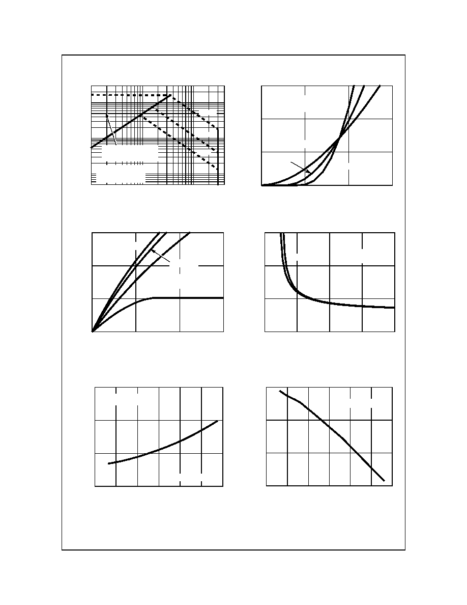
Typical Characteristic
T
A
= 25∞C unless otherwise noted
Figure 1. Normalized Power Dissipation vs
Ambient Temperature
Figure 2. Maximum Continuous Drain Current vs
Ambient Temperature
Figure 3. Normalized Maximum Transient Thermal Impedance
Figure 4. Peak Current Capability
T
A
, AMBIENT TEMPERATURE (
o
C)
P
O
W
E
R DIS
S
I
P
A
T
ION M
U
L
T
IP
L
I
E
R
0
0
25
50
75
100
150
0.2
0.4
0.6
0.8
1.0
1.2
125
0
2
4
6
8
10
25
50
75
100
125
150
ID
, DRAIN CUR
RENT
(
A
)
T
A
, AMBIENT TEMPERATURE (
o
C)
V
GS
= 4.5V
V
GS
= 2.5V
0.01
0.1
1
10
-4
10
-3
10
-2
10
-1
10
0
10
1
10
2
10
3
2
10
-5
t, RECTANGULAR PULSE DURATION (s)
Z
JA
,
NORM
A
L
IZ
E
D
TH
ERM
A
L I
M
PED
AN
CE
NOTES:
DUTY FACTOR: D = t
1
/t
2
PEAK T
J
= P
DM
x Z
JA
x R
JA
+ T
A
P
DM
t
1
t
2
0.5
0.2
0.1
0.05
0.01
0.02
DUTY CYCLE - DESCENDING ORDER
I
DM
, PE
AK CURRENT
(
A
)
t, PULSE WIDTH (s)
10
100
10
-5
10
-4
10
-3
10
-2
10
-1
10
0
10
1
10
2
10
3
500
5
T
A
= 25
o
C
I = I
25
150 - T
A
125
FOR TEMPERATURES
ABOVE 25
o
C DERATE PEAK
CURRENT AS FOLLOWS:
TRANSCONDUCTANCE
MAY LIMIT CURRENT
IN THIS REGION
V
GS
= 2.5V
FDW2601NZ Rev. A
www.fairchildsemi.com
FDW2601NZ D
u
al
N-Channel 2.
5V Speci
fie
d
Power
T
re
n
c
hÆ MOSFET
5
Figure 5. Forward Bias Safe Operating Area
Figure 6. Transfer Characteristics
Figure 7. Saturation Characteristics
Figure 8. Drain to Source On Resistance vs Gate
Voltage and Drain Current
Figure 9. Normalized Drain to Source On
Resistance vs Junction Temperature
Figure 10. Normalized Gate Threshold Voltage vs
Junction Temperature
Typical Characteristic
(Continued) T
A
= 25∞C unless otherwise noted
1
10
100
0.1
1
10
40
0.5
300
V
DS
, DRAIN TO SOURCE VOLTAGE (V)
I
D
, DRAIN CURRE
NT
(
A
)
T
J
= MAX RATED
T
A
= 25
o
C
SINGLE PULSE
LIMITED BY r
DS(ON)
AREA MAY BE
OPERATION IN THIS
100
µ
s
10ms
1ms
0
20
40
60
1.0
1.5
2.0
2.5
I
D
,
D
RAIN CURRENT
(
A
)
V
GS
, GATE TO SOURCE VOLTAGE (V)
PULSE DURATION = 80
µ
s
DUTY CYCLE = 0.5% MAX
V
DD
= 10V
T
J
= 150
o
C
T
J
= 25
o
C
T
J
= -55
o
C
0
20
40
60
0
0.5
1.0
1.5
I
D
, DRAIN CURREN
T
(
A
)
V
DS
, DRAIN TO SOURCE VOLTAGE (V)
V
GS
= 2.5V
PULSE DURATION = 80
µ
s
DUTY CYCLE = 0.5% MAX
V
GS
= 1.8V
T
A
= 25
o
C
V
GS
= 4.5V
V
GS
= 10V
0
15
30
45
1
2
3
4
5
I
D
= 1A
V
GS
, GATE TO SOURCE VOLTAGE (V)
I
D
= 8.2A
r
DS
(
O
N
)
,
DR
AI
N
T
O
SOURCE
ON RES
I
ST
ANCE
(
m
)
PULSE DURATION = 80
µ
s
DUTY CYCLE = 0.5% MAX
0.5
1.0
1.5
2.0
-80
-40
0
40
80
120
160
NORM
AL
IZ
E
D
DRAIN T
O
SOUR
CE
T
J
, JUNCTION TEMPERATURE (
o
C)
O
N
R
ESI
ST
A
NCE
V
GS
= 4.5V, I
D
= 8.2A
PULSE DURATION = 80
µ
s
DUTY CYCLE = 0.5% MAX
0.50
0.75
1.00
1.25
-80
-40
0
40
80
120
160
NORM
AL
I
Z
ED GA
T
E
T
J
, JUNCTION TEMPERATURE (
o
C)
V
GS
= V
DS
, I
D
= 250
µ
A
T
HRES
H
OL
D V
O
L
T
A
GE

FDW2601NZ Rev. A
www.fairchildsemi.com
FDW2601NZ D
u
al
N-Channel 2.
5V Speci
fie
d
Power
T
re
n
c
hÆ MOSFET
6
Figure 11. Normalized Drain to Source
Breakdown Voltage vs Junction Temperature
Figure 12. Capacitance vs Drain to Source
Voltage
Figure 13. Gate Charge Waveforms for Constant Gate Currents
Typical Characteristic
(Continued) T
A
= 25∞C unless otherwise noted
0.90
0.95
1.00
1.05
1.10
-80
-40
0
40
80
120
160
T
J
, JUNCTION TEMPERATURE (
o
C)
NORM
AL
IZ
E
D
DRAIN T
O
S
O
UR
CE
I
D
= 250
µ
A
BRE
AKDO
W
N
V
O
L
T
A
GE
100
1000
0.1
1
10
4000
30
C, CAP
A
C
I
T
ANCE (
p
F
)
V
DS
, DRAIN TO SOURCE VOLTAGE (V)
V
GS
= 0V, f = 1MHz
C
ISS
= C
GS
+ C
GD
C
OSS
C
DS
+ C
GD
C
RSS
= C
GD
0
1.5
3.0
4.5
0
5
10
15
20
25
V
GS
, GA
T
E
T
O
SOURCE V
O
L
T
A
GE (
V
)
Qg, GATE CHARGE (nC)
V
DD
= 15V
I
D
= 1A
I
D
= 8.2A
WAVEFORMS IN
DESCENDING ORDER:
FDW2601NZ Rev. A
www.fairchildsemi.com
FDW2601NZ D
u
al
N-Channel 2.
5V Speci
fie
d
Power
T
re
n
c
hÆ MOSFET
7
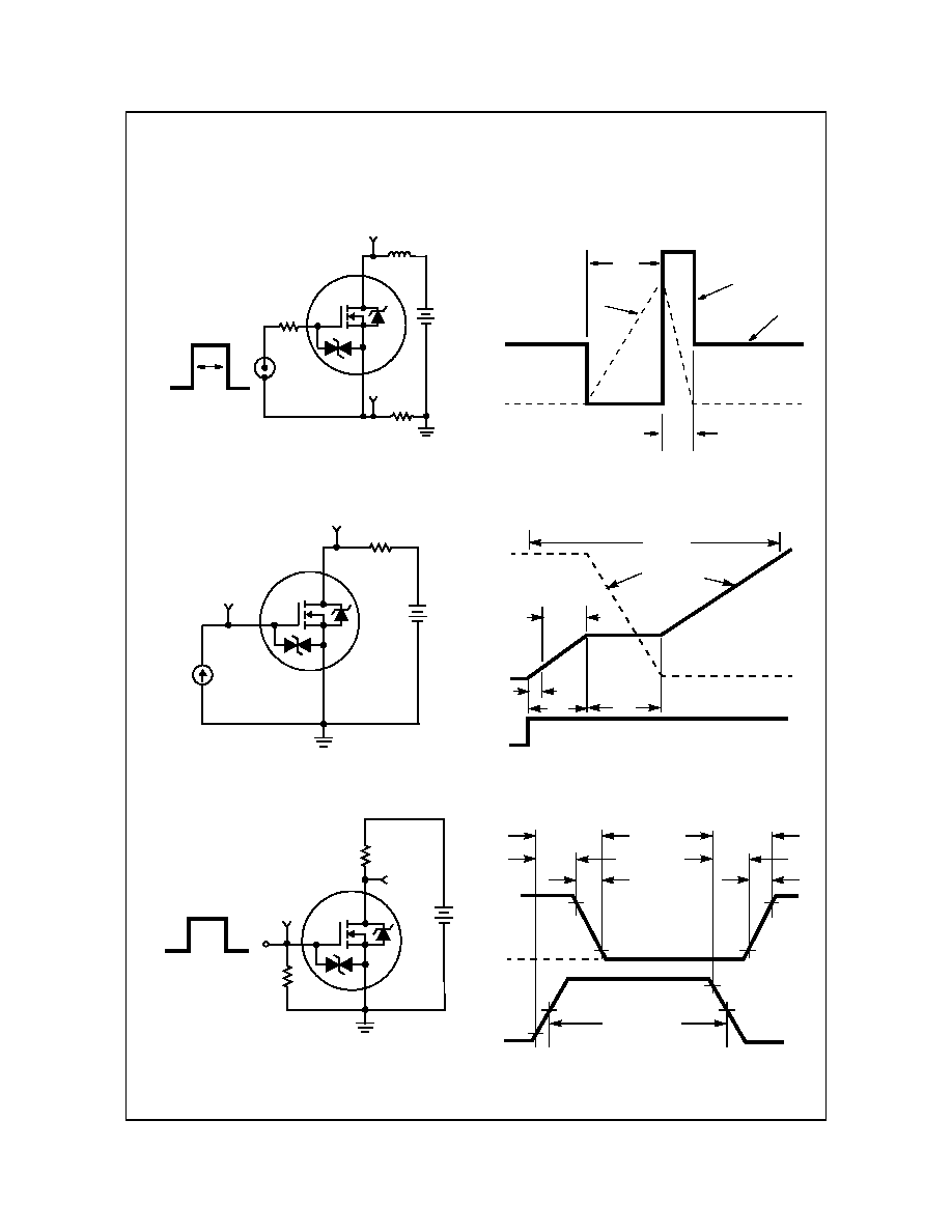
Test Circuits and Waveforms
Figure 14. Unclamped Energy Test Circuit
Figure 15. Unclamped Energy Waveforms
Figure 16. Gate Charge Test Circuit
Figure 17. Gate Charge Waveforms
Figure 18. Switching Time Test Circuit
Figure 19. Switching Time Waveforms
t
P
V
GS
0.01
L
I
AS
+
-
V
DS
V
DD
R
G
DUT
VARY t
P
TO OBTAIN
REQUIRED PEAK I
AS
0V
V
DD
V
DS
BV
DSS
t
P
I
AS
t
AV
0
R
L
V
GS
+
-
V
DS
V
DD
DUT
I
g(REF)
V
DD
Q
g(TH)
V
GS
= 1V
Q
gs2
Q
g(TOT)
V
GS
= 4.5V
V
DS
V
GS
I
g(REF)
0
0
Q
gs
Q
gd
V
GS
0V
R
GS
R
L
DUT
+
-
V
GS
V
DS
t
ON
t
d(ON)
t
r
90%
10%
V
DS
90%
10%
t
f
t
d(OFF)
t
OFF
90%
50%
50%
10%
PULSE WIDTH
V
GS
0
0

FDW2601NZ Rev. A
www.fairchildsemi.com
FDW2601NZ D
u
al
N-Channel 2.
5V Speci
fie
d
Power
T
re
n
c
hÆ MOSFET
8
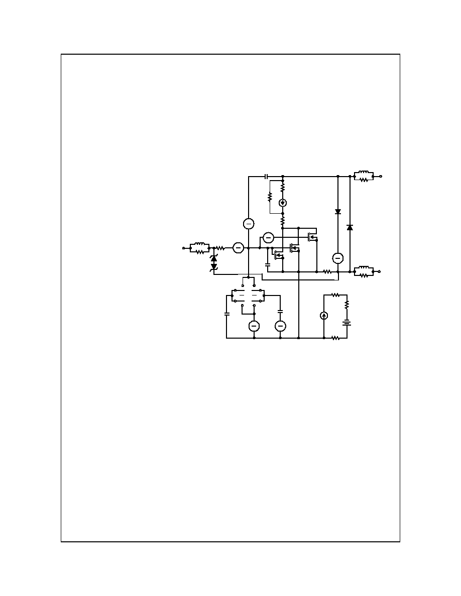
PSPICE Electrical Model
.SUBCKT FDW2601NZ 2 1 3 ;
rev June 2004
CA 12 8 19.3e-10
CB 15 14 19.3e-10
CIN 6 8 1.7e-9
DBODY 5 7 DBODYMOD
DBREAK 7 11 DBREAKMOD
DPLCAP 10 5 DPLCAPMOD
DESD1 91 9 DESD1MOD
DESD2 91 7 DESD2MOD
EBREAK 5 11 17 18 33.3
EDS 14 8 5 8 1
EGS 13 8 6 8 1
ESG 6 10 8 6 1
EVTHRES 6 21 19 8 1
EVTEMP 6 20 18 22 1
IT 8 17 1
LDRAIN 2 5 1e-9
LGATE 1 9 0.96e-9
LSOURCE 3 7 0.19e-9
RLDRAIN 2 5 10
RLGATE 1 9 9.6
RLSOURCE 3 7 1.9
MMED 16 6 8 8 MMEDMOD
MSTRO 16 6 8 8 MSTROMOD
MWEAK 16 21 8 8 MWEAKMOD
RBREAK 17 18 RBREAKMOD 1
RDRAIN 50 16 RDRAINMOD 8.8e-3
RGATE 9 20 2.75
RSLC1 5 51 RSLCMOD 1e-6
RSLC2 5 50 1e3
RSOURCE 8 7 RSOURCEMOD 3e-4
RVTHRES 22 8 RVTHRESMOD 1
RVTEMP 18 19 RVTEMPMOD 1
S1A 6 12 13 8 S1AMOD
S1B 13 12 13 8 S1BMOD
S2A 6 15 14 13 S2AMOD
S2B 13 15 14 13 S2BMOD
VBAT 22 19 DC 1
ESLC 51 50 VALUE={(V(5,51)/ABS(V(5,51)))*(PWR(V(5,51)/(1e-6*120),2.5))}
.MODEL DBODYMOD D (IS = 18.6e-12 N=0.93 RS = 6.6e-3 IKF=0.2 TRS1 = 1.7e-3 TRS2 = 2e-6 XTI=0.1 TIKF=0.001
CJO =5.2e-10 TT=8.7e-9 M = 0.58)
.MODEL DBREAKMOD D (RS = 1e-1 TRS1 = 9e-3 TRS2 = -2e-5)
.MODEL DPLCAPMOD D (CJO = 0.76e-9 IS = 1e-30 N = 10 M = 0.58)
.MODEL DESD1MOD D (BV=10.5 TBV1=-0.0018 N=9.4 RS=5)
.MODEL DESD2MOD D (BV=10.5 TBV1=-0.0018 N=9.4 RS=5)
.MODEL MMEDMOD NMOS (VTO = 1.0 KP = 1.7 IS=1e-30 N = 10 TOX = 1 L = 1u W = 1u RG = 2.75)
.MODEL MSTROMOD NMOS (VTO = 1.27 KP = 147 IS = 1e-30 N = 10 TOX = 1 L = 1u W = 1u)
.MODEL MWEAKMOD NMOS (VTO = 0.83 KP = 0.05 IS = 1e-30 N = 10 TOX = 1 L = 1u W = 1u RG = 27.5 RS = 0.1)
.MODEL RBREAKMOD RES (TC1 = 8.8e-4 TC2 = -13e-7)
.MODEL RDRAINMOD RES (TC1 = 1e-9 TC2 = 1e-5)
.MODEL RSLCMOD RES (TC1 = 2e-9 TC2 = 5e-8)
.MODEL RSOURCEMOD RES (TC1 = 8.2e-2 TC2 = 1e-6)
.MODEL RVTHRESMOD RES (TC1 = -13e-4 TC2 = -2.8e-6)
.MODEL RVTEMPMOD RES (TC1 = -1.3e-3 TC2 = 1e-6)
.MODEL S1AMOD VSWITCH (RON = 1e-5 ROFF = 0.1 VON = -6 VOFF= -1.5)
.MODEL S1BMOD VSWITCH (RON = 1e-5 ROFF = 0.1 VON = -1.5 VOFF= -6)
.MODEL S2AMOD VSWITCH (RON = 1e-5 ROFF = 0.1 VON = -0.5 VOFF= 0.3)
.MODEL S2BMOD VSWITCH (RON = 1e-5 ROFF = 0.1 VON = 0.3 VOFF= -0.5)
ENDS
Note: For further discussion of the PSPICE model, consult A New PSPICE Sub-Circuit for the Power MOSFET Featuring Global
Temperature Options; IEEE Power Electronics Specialist Conference Records, 1991, written by William J. Hepp and C. Frank
Wheatley.
+
-
6
8
+
-
5
51
+
-
19
8
+
-
17
18
6
8
+
-
5
8
+
-
RBREAK
RVTEMP
VBAT
RVTHRES
IT
17
18
19
22
12
13
15
S1A
S1B
S2A
S2B
CA
CB
EGS
EDS
14
8
13
8
14
13
MWEAK
EBREAK
DBODY
RSOURCE
SOURCE
11
7
3
LSOURCE
RLSOURCE
CIN
RDRAIN
EVTHRES
16
21
8
MMED
MSTRO
DRAIN
2
LDRAIN
RLDRAIN
DBREAK
DPLCAP
ESLC
RSLC1
10
5
51
50
RSLC2
1
GATE
RGATE
EVTEMP
9
ESG
LGATE
RLGATE
20
+
-
+
-
+
-
18
22
DESD1
DESD2
91
6
FDW2601NZ Rev. A
www.fairchildsemi.com
FDW2601NZ D
u
al
N-Channel 2.
5V Speci
fie
d
Power
T
re
n
c
hÆ MOSFET
9
SABER Electrical Model
REV June 2004
template fdw2601nz n2,n1,n3
electrical n2,n1,n3
{
var i iscl
dp..model dbodymod = (isl = 18.6e-12, nl=0.93, rs = 6.6e-3, trs1 = 1.7e-3, trs2 = 2e-6, xti=0.1, cjo = 5.2e-10, ikf=0.2, tt = 8.7e-9,
m = 0.58, tikf=0.001)
dp..model dbreakmod = (rs = 1e-1, trs1 = 9e-3, trs2 = -2.0e-5)
dp..model dplcapmod = (cjo = 0.76e-9, isl=10e-30, nl=10, m=0.58)
dp..model desd1mod = (bv=10.5, tbv1=-0.0018, nl=9.4, rs=5)
dp..model desd2mod = (bv=10.5, tbv1=-0.0018, nl=9.4, rs=5)
m..model mmedmod = (type=_n, vto = 1.0, kp=1.7, is=1e-30, tox=1)
m..model mstrongmod = (type=_n, vto = 1.27, kp = 147, is = 1e-30, tox = 1)
m..model mweakmod = (type=_n, vto = 0.83, kp = 0.05, is = 1e-30, tox = 1, rs=0.1)
sw_vcsp..model s1amod = (ron = 1e-5, roff = 0.1, von = -6, voff = -1.5)
sw_vcsp..model s1bmod = (ron = 1e-5, roff = 0.1, von = -1.5, voff = -6 )
sw_vcsp..model s2amod = (ron = 1e-5, roff = 0.1, von = -0.5, voff = 0.3)
sw_vcsp..model s2bmod = (ron = 1e-5, roff = 0.1, von = 0.3, voff = -0.5)
c.ca n12 n8 = 19.3e-10
c.cb n15 n14 = 19.3e-10
c.cin n6 n8 = 1.7e-9
dp.dbody n7 n5 = model=dbodymod
dp.dbreak n5 n11 = model=dbreakmod
dp.dplcap n10 n5 = model=dplcapmod
dp.desd1 n91 n9 = model=desd1mod
dp.desd2 n91 n7 = model=desd2mod
spe.ebreak n11 n7 n17 n18 = 33.3
spe.eds n14 n8 n5 n8 = 1
spe.egs n13 n8 n6 n8 = 1
spe.esg n6 n10 n6 n8 = 1
spe.evtemp n20 n6 n18 n22 = 1
spe.evthres n6 n21 n19 n8 = 1
i.it n8 n17 = 1
l.ldrain n2 n5 = 1e-9
l.lgate n1 n9 = 0.96e-9
l.lsource n3 n7 = 0.19e-9
res.rldrain n2 n5 = 10
res.rlgate n1 n9 = 9.6
res.rlsource n3 n7 = 1.9
m.mmed n16 n6 n8 n8 = model=mmedmod, l=1u, w=1u
m.mstrong n16 n6 n8 n8 = model=mstrongmod, l=1u, w=1u
m.mweak n16 n21 n8 n8 = model=mweakmod, l=1u, w=1u
res.rbreak n17 n18 = 1, tc1 = 8.8e-4, tc2 = -13e-7
res.rdrain n50 n16 = 8.8e-3, tc1 = 1e-9, tc2 = 1e-5
res.rgate n9 n20 = 2.75
res.rslc1 n5 n51= 1e-6, tc1 = 2e-9, tc2 =5e-8
res.rslc2 n5 n50 = 1e3
res.rsource n8 n7 = 3e-4, tc1 = 8.2e-2, tc2 =1e-6
res.rvtemp n18 n19 = 1, tc1 = -1.3e-3, tc2 = 1e-6
res.rvthres n22 n8 = 1, tc1 = -13e-4, tc2 = -2.8e-6
sw_vcsp.s1a n6 n12 n13 n8 = model=s1amod
sw_vcsp.s1b n13 n12 n13 n8 = model=s1bmod
sw_vcsp.s2a n6 n15 n14 n13 = model=s2amod
sw_vcsp.s2b n13 n15 n14 n13 = model=s2bmod
v.vbat n22 n19 = dc=1
equations {
i (n51->n50) +=iscl
iscl: v(n51,n50) = ((v(n5,n51)/(1e-9+abs(v(n5,n51))))*((abs(v(n5,n51)*1e6/120))** 2.5))
}
}
18
22
+
-
6
8
+
-
19
8
+
-
17
18
6
8
+
-
5
8
+
-
RBREAK
RVTEMP
VBAT
RVTHRES
IT
17
18
19
22
12
13
15
S1A
S1B
S2A
S2B
CA
CB
EGS
EDS
14
8
13
8
14
13
MWEAK
EBREAK
DBODY
RSOURCE
SOURCE
11
7
3
LSOURCE
RLSOURCE
CIN
RDRAIN
EVTHRES
16
21
8
MMED
MSTRO
DRAIN
2
LDRAIN
RLDRAIN
DBREAK
DPLCAP
ISCL
RSLC1
10
5
51
50
RSLC2
1
GATE
RGATE
EVTEMP
9
ESG
LGATE
RLGATE
20
+
-
+
-
+
-
6
DESD1
DESD2
91

FDW2601NZ Rev. A
www.fairchildsemi.com
FDW2601NZ D
u
al
N-Channel 2.
5V Speci
fie
d
Power
T
re
n
c
hÆ MOSFET
10
SPICE Thermal Model
REV June 2004
FDW2601NZ_JA Junction Ambient
Minimum copper pad area
CTHERM1 Junction c2 5.7e-4
CTHERM2 c2 c3 5.72e-4
CTHERM3 c3 c4 5.8e-4
CTHERM4 c4 c5 4.7e-3
CTHERM5 c5 c6 5.1e-3
CTHERM6 c6 c7 0.02
CTHERM7 c7 c8 0.2
CTHERM8 c8 Ambient 6
RTHERM1 Junction c2 0.003
RTHERM2 c2 c3 0.25
RTHERM3 c3 c4 1.0
RTHERM4 c4 c5 1.1
RTHERM5 c5 c6 7.5
RTHERM6 c6 c7 33.6
RTHERM7 c7 c8 33.7
RTHERM8 c8 Ambient 33.8
SABER Thermal Model
SABER thermal model FDW2601NZ
Minimum copper pad area
template thermal_model th tl
thermal_c th, tl
{
ctherm.ctherm1 th c2 = 5.7e-4
ctherm.ctherm2 c2 c3 = 5.72e-4
ctherm.ctherm3 c3 c4 = 5.8e-4
ctherm.ctherm4 c4 c5 = 4.7e-3
ctherm.ctherm5 c5 c6 = 5.1e-3
ctherm.ctherm6 c6 c7 = 0.02
ctherm.ctherm7 c7 c8 = 0.2
ctherm.ctherm8 c8 tl = 6
rtherm.rtherm1 th c2 = 0.003
rtherm.rtherm2 c2 c3 = 0.25
rtherm.rtherm3 c3 c4 = 1.0
rtherm.rtherm4 c4 c5 = 1.1
rtherm.rtherm5 c5 c6 = 7.5
rtherm.rtherm6 c6 c7 = 33.6
rtherm.rtherm7 c7 c8 = 33.7
rtherm.rtherm8 c8 tl = 33.8
}
RTHERM6
RTHERM8
RTHERM7
RTHERM5
RTHERM4
RTHERM3
CTHERM4
CTHERM6
CTHERM5
CTHERM3
CTHERM2
CTHERM1
tl
8
7
6
5
4
3
JUNCTION
AMBIENT
2
th
RTHERM2
RTHERM1
CTHERM7
CTHERM8

www.fairchildsemi.com
TRADEMARKS
The following are registered and unregistered trademarks Fairchild Semiconductor owns or is authorized to use and is not
intended to be an exhaustive list of all such trademarks.
DISCLAIMER
FAIRCHILD SEMICONDUCTOR RESERVES THE RIGHT TO MAKE CHANGES WITHOUT FURTHER NOTICE TO ANY
PRODUCTS HEREIN TO IMPROVE RELIABILITY, FUNCTION OR DESIGN. FAIRCHILD DOES NOT ASSUME ANY
LIABILITY ARISING OUT OF THE APPLICATION OR USE OF ANY PRODUCT OR CIRCUIT DESCRIBED HEREIN;
NEITHER DOES IT CONVEY ANY LICENSE UNDER ITS PATENT RIGHTS, NOR THE RIGHTS OF OTHERS.
LIFE SUPPORT POLICY
FAIRCHILD'S PRODUCTS ARE NOT AUTHORIZED FOR USE AS CRITICAL COMPONENTS IN LIFE SUPPORT
DEVICES OR SYSTEMS WITHOUT THE EXPRESS WRITTEN APPROVAL OF FAIRCHILD SEMICONDUCTOR
CORPORATION.
As used herein:
1. Life support devices or systems are devices or systems
which, (a) are intended for surgical implant into the body,
or (b) support or sustain life, or (c) whose failure to perform
when properly used in accordance with instructions for use
provided in the labeling, can be reasonably expected to
result in significant injury to the user.
2. A critical component is any component of a life support
device or system whose failure to perform can be
reasonably expected to cause the failure of the life support
device or system, or to affect its safety or effectiveness.
PRODUCT STATUS DEFINITIONS
Definition of Terms
ACExTM
ActiveArrayTM
BottomlessTM
CoolFETTM
CROSSVOLTTM
DOMETM
EcoSPARKTM
E
2
CMOSTM
EnSignaTM
FACTTM
FACT Quiet SeriesTM
FAST
Æ
FASTrTM
FPSTM
FRFETTM
GlobalOptoisolatorTM
GTOTM
HiSeCTM
I
2
CTM
i-Lo
TM
ImpliedDisconnect
TM
IntelliMAXTM
ISOPLANARTM
LittleFETTM
MICROCOUPLERTM
MicroFETTM
MicroPakTM
MICROWIRETM
MSX
TM
MSXPro
TM
OCX
TM
OCXPro
TM
OPTOLOGIC
Æ
OPTOPLANARTM
PACMANTM
POPTM
Power247TM
PowerEdgeTM
PowerSaverTM
PowerTrench
Æ
QFET
Æ
QSTM
QT OptoelectronicsTM
Quiet SeriesTM
RapidConfigure
TM
RapidConnect
TM
µSerDes
TM
SILENT SWITCHER
Æ
SMART STARTTM
SPMTM
StealthTM
SuperFETTM
SuperSOTTM-3
SuperSOTTM-6
SuperSOTTM-8
SyncFETTM
TinyLogic
Æ
TINYOPTOTM
TruTranslationTM
UHCTM
UltraFET
Æ
UniFETTM
VCXTM
Across the board. Around the world.
TM
The Power Franchise
Æ
Programmable Active DroopTM
Datasheet Identification
Product Status
Definition
Advance Information
Formative or In
Design
This datasheet contains the design specifications for
product development. Specifications may change in
any manner without notice.
Preliminary
First Production
This datasheet contains preliminary data, and
supplementary data will be published at a later date.
Fairchild Semiconductor reserves the right to make
changes at any time without notice in order to improve
design.
No Identification Needed
Full Production
This datasheet contains final specifications. Fairchild
Semiconductor reserves the right to make changes at
any time without notice in order to improve design.
Obsolete
Not In Production
This datasheet contains specifications on a product
that has been discontinued by Fairchild semiconductor.
The datasheet is printed for reference information only.
FDW2601NZ Rev. A
FDW2601NZ D
u
al
N-Channel 2.
5V Speci
fie
d
Power
T
re
n
c
hÆ MOSFET
11