 | ÐлекÑÑоннÑй компоненÑ: FDY300NZ | СкаÑаÑÑ:  PDF PDF  ZIP ZIP |
Äîêóìåíòàöèÿ è îïèñàíèÿ www.docs.chipfind.ru
January 2006
©
2006 Fairchild Semiconductor Corporation
www.fairchildsemi.com
FDY300NZ Rev A
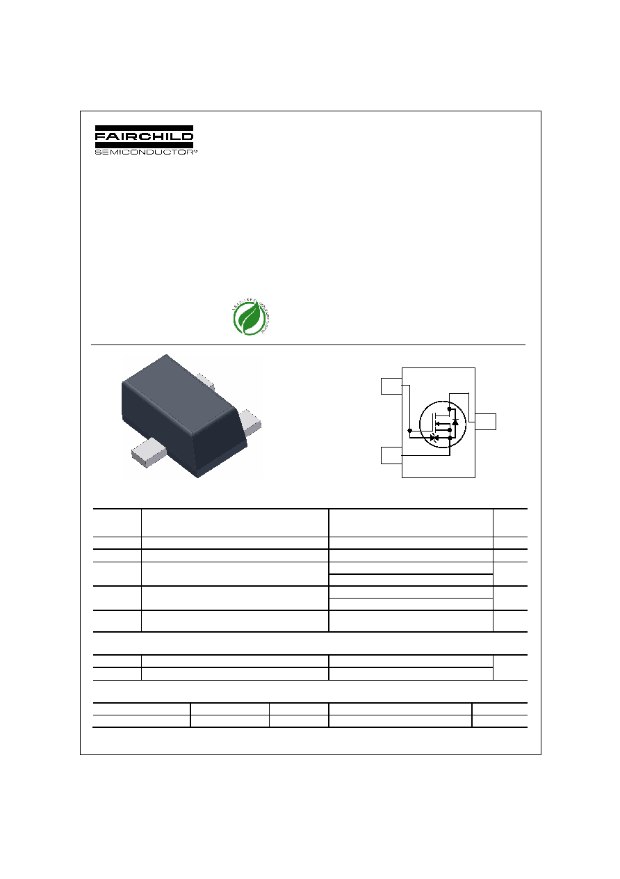
FDY300NZ
Single N-Channel 2.5V Specified PowerTrench
®
®
®
®
MOSFET
General Description
This Single N-Channel MOSFET has been designed
using Fairchild Semiconductor's advanced Power
Trench process to optimize the R
DS(ON)
@ V
GS
= 2.5v.
Applications
·
Li-Ion Battery Pack
Features
·
600 mA, 20 V R
DS(ON)
= 700 m
@ V
GS
= 4.5 V
R
DS(ON)
= 850 m
@ V
GS
= 2.5 V
·
ESD protection diode (note 3)
·
RoHS Compliant
Absolute Maximum Ratings
T
A
=25
o
C unless otherwise noted
Symbol
Parameter
Ratings
Unit
s
V
DSS
Drain-Source Voltage
20
V
V
GSS
Gate-Source Voltage
±
12
V
I
D
Drain Current Continuous
(Note 1a) 1a)
600
mA
Pulsed
1000
P
D
Power Dissipation (Steady State)
(Note 1a) 1a)
625
mW
(Note 1b) 1
446
T
J
, T
STG
Operating and Storage Junction Temperature
Range
55 to +150
°
C
Thermal Characteristics
R
JA
Thermal Resistance, Junction-to-Ambient
(Note 1a) 1a)
200
°
C/W
R
JA
Thermal Resistance, Junction-to-Ambient
(Note 1b) 1
280
Package Marking and Ordering Information
Device Marking
Device
Reel Size
Tape width
Quantity
C
FDY300NZ
7 ''
8 mm
3000 units
F
D
Y
3
0
0
N
Z
S
i
n
g
l
e
N
-
C
h
a
n
n
e
l
2
.
5
V
S
p
e
c
i
f
i
e
d
P
o
w
e
r
T
r
e
n
c
h
®
®
®
®
M
O
S
F
E
T
1
2
3
G
D
S
1 S
G
D
FDY300NZ Rev A www.fairchildsemi.com
Electrical Characteristics
T
A
= 25°C unless otherwise noted
Symbol
Parameter
Test Conditions
Min Typ Max Units
Off Characteristics
BV
DSS
DrainSource Breakdown
Voltage
V
GS
= 0 V,
I
D
= 250
µ
A
20
V
BV
DSS
T
J
Breakdown Voltage Temperature
Coefficient
I
D
= 250
µ
A, Referenced to 25
°
C
15
mV/
°
C
I
DSS
Zero Gate Voltage Drain Current V
DS
= 16 V,
V
GS
= 0 V
1
µ
A
V
GS
=
±
12 V, V
DS
= 0 V
±
10
µ
A
I
GSS
GateBody Leakage,
V
GS
=
±
4.5 V, V
DS
= 0 V
±
1
µ
A
On Characteristics
(Note 2)
V
GS(th)
Gate Threshold Voltage
V
DS
= V
GS
,
I
D
= 250
µ
A
0.6
1.0
1.5
V
V
GS(th)
T
J
Gate Threshold Voltage
Temperature Coefficient
I
D
= 250
µ
A, Referenced to 25
°
C
3
mV/
°
C
R
DS(on)
Static DrainSource
OnResistance
V
GS
= 4.5 V,
I
D
= 600 mA
V
GS
= 2.5 V,
I
D
= 500 mA
V
GS
= 1.8 V,
I
D
= 150 mA
V
GS
= 4.5 V, I
D
=600mA, T
J
= 125
°
C
0.24
0.36
0.70
0.35
0.70
0.85
1.25
1.00
g
FS
Forward Transconductance
V
DS
= 5 V,
I
D
= 600 mA
1.8
S
Dynamic Characteristics
C
iss
Input Capacitance
60
pF
C
oss
Output Capacitance
20
pF
C
rss
Reverse Transfer Capacitance
V
DS
= 10 V,
V
GS
= 0 V,
f = 1.0 MHz
10
pF
Switching Characteristics
(Note 2)
t
d(on)
TurnOn Delay Time
6
12
ns
t
r
TurnOn Rise Time
8
16
ns
t
d(off)
TurnOff Delay Time
8
16
ns
t
f
TurnOff Fall Time
V
DD
= 10 V,
I
D
= 1 A,
V
GS
= 4.5 V,
R
GEN
= 6
2.4
4.8
ns
Q
g
Total Gate Charge
0.8
1.1
nC
Q
gs
GateSource Charge
0.16
nC
Q
gd
GateDrain Charge
V
DS
= 10 V,
I
D
= 600 mA,
V
GS
= 4.5 V
0.26
nC
DrainSource Diode Characteristics and Maximum Ratings
V
SD
DrainSource Diode Forward
Voltage
V
GS
= 0 V, I
S
= 150 mA
(Note 2)
0.7
1.2
V
t
rr
Diode Reverse Recovery Time
8
nS
Q
rr
Diode Reverse Recovery Charge
I
F
= 600 mA,
dI
F
/dt = 100 A/µs
1
nC
Notes:
1.
R
JA
is the sum of the junction-to-case and case-to-ambient thermal resistance where the case thermal reference is defined as the solder mounting surface of
the drain pins. R
JC
is guaranteed by design while R
CA
is determined by the user's board design.
a)
200°C/W when
mounted on a 1in
2
pad
of 2 oz copper
b) 280°C/W when mounted on a
minimum pad of 2 oz copper
Scale 1 : 1 on letter size paper
2
.
Pulse Test: Pulse Width < 300
µ
s,
Duty Cycle < 2.0%
3. The diode connected between the gate
and source serves only as protection
againts ESD. No gate overvoltage
rating is implied.
F
D
Y
3
0
0
N
Z
S
i
n
g
l
e
N
-
C
h
a
n
n
e
l
2
.
5
V
S
p
e
c
i
f
i
e
d
P
o
w
e
r
T
r
e
n
c
h
®
®
®
®
M
O
S
F
E
T
FDY300NZ Rev A www.fairchildsemi.com
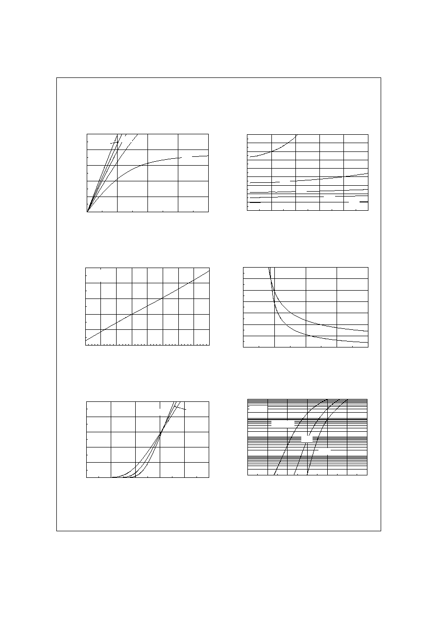
Typical Characteristics
0
0.2
0.4
0.6
0.8
1
0
0.25
0.5
0.75
1
V
DS
, DRAIN-SOURCE VOLTAGE (V)
I
D
,
D
R
A
I
N
C
U
R
R
E
N
T
(
A
)
2.5V
2.0V
V
GS
= 4.5V
3.0V
3.5V
0.8
1
1.2
1.4
1.6
1.8
2
2.2
2.4
2.6
0
0.2
0.4
0.6
0.8
1
I
D
, DRAIN CURRENT (A)
R
D
S
(
O
N
)
,
N
O
R
M
A
L
I
Z
E
D
D
R
A
I
N
-
S
O
U
R
C
E
O
N
-
R
E
S
I
S
T
A
N
C
E
V
GS
= 2.0V
2.5V
3.5V
4.5V
3.0V
Figure 1. On-Region Characteristics.
Figure 2. On-Resistance Variation with
Drain Current and Gate Voltage.
0.6
0.8
1
1.2
1.4
1.6
-50
-25
0
25
50
75
100
125
150
T
J
, JUNCTION TEMPERATURE (
o
C)
R
D
S
(
O
N
)
,
N
O
R
M
A
L
I
Z
E
D
D
R
A
I
N
-
S
O
U
R
C
E
O
N
-
R
E
S
I
S
T
A
N
C
E
I
D
= 600mA
V
GS
= 4.5V
0.2
0.3
0.4
0.5
0.6
0.7
0.8
0.9
1
2
3
4
5
V
GS
, GATE TO SOURCE VOLTAGE (V)
R
D
S
(
O
N
)
,
O
N
-
R
E
S
I
S
T
A
N
C
E
(
O
H
M
)
I
D
= 300mA
T
A
= 125
o
C
T
A
= 25
o
C
Figure 3. On-Resistance Variation with
Temperature.
Figure 4. On-Resistance Variation with
Gate-to-Source Voltage.
0
0.3
0.6
0.9
1.2
1.5
0.5
1
1.5
2
2.5
3
V
GS
, GATE TO SOURCE VOLTAGE (V)
I
D
,
D
R
A
I
N
C
U
R
R
E
N
T
(
A
)
T
A
= -55
o
C
25
o
C
125
o
C
V
DS
= 5V
0.0001
0.001
0.01
0.1
1
0
0.2
0.4
0.6
0.8
1
1.2
V
SD
, BODY DIODE FORWARD VOLTAGE (V)
I
S
,
R
E
V
E
R
S
E
D
R
A
I
N
C
U
R
R
E
N
T
(
A
)
T
A
= 125
o
C
25
o
C
-55
o
C
V
GS
= 0V
Figure 5. Transfer Characteristics.
Figure 6. Body Diode Forward Voltage Variation
with Source Current and Temperature.
F
D
Y
3
0
0
N
Z
S
i
n
g
l
e
N
-
C
h
a
n
n
e
l
2
.
5
V
S
p
e
c
i
f
i
e
d
P
o
w
e
r
T
r
e
n
c
h
®
®
®
®
M
O
S
F
E
T
FDY300NZ Rev A www.fairchildsemi.com
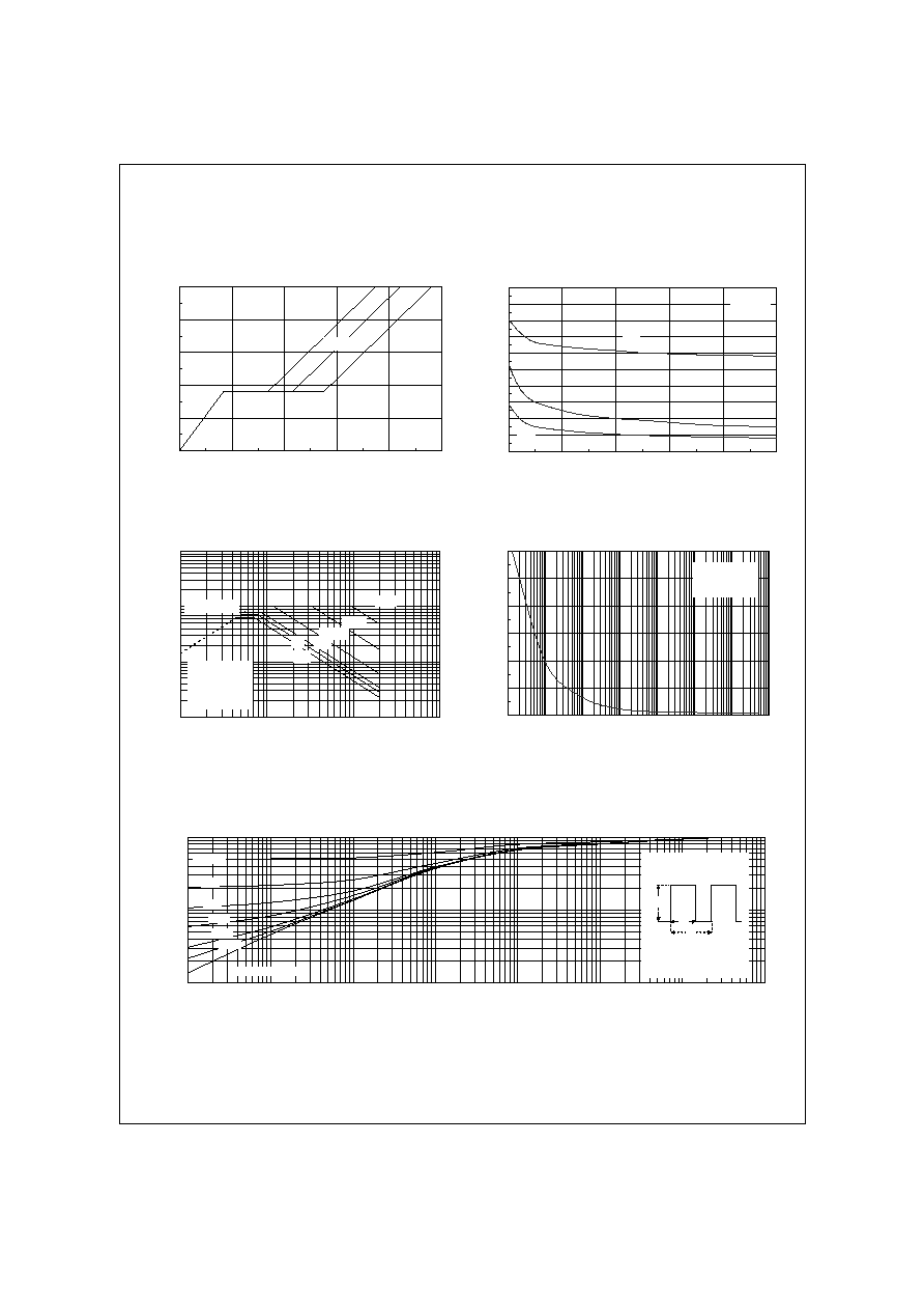
Typical Characteristics
0
1
2
3
4
5
0
0.2
0.4
0.6
0.8
1
Q
g
, GATE CHARGE (nC)
V
G
S
,
G
A
T
E
-
S
O
U
R
C
E
V
O
L
T
A
G
E
(
V
)
I
D
= 600mA
V
DS
= 5V
15V
10V
0
10
20
30
40
50
60
70
80
90
100
0
4
8
12
16
20
V
DS
, DRAIN TO SOURCE VOLTAGE (V)
C
A
P
A
C
I
T
A
N
C
E
(
p
F
)
C
iss
C
rss
C
oss
f = 1MHz
V
GS
= 0 V
Figure 7. Gate Charge Characteristics.
Figure 8. Capacitance Characteristics.
0.01
0.1
1
10
0.1
1
10
100
V
DS
, DRAIN-SOURCE VOLTAGE (V)
I
D
,
D
R
A
I
N
C
U
R
R
E
N
T
(
A
)
DC
10s
1s
100ms
R
DS(ON)
LIMIT
V
GS
= 4.5V
SINGLE PULSE
R
JA
= 280
o
C/W
T
A
= 25
o
C
10ms
1ms
0
5
10
15
20
25
30
0.0001
0.001
0.01
0.1
1
10
100
1000
t
1
, TIME (sec)
P
(
p
k
)
,
P
E
A
K
T
R
A
N
S
I
E
N
T
P
O
W
E
R
(
W
)
SINGLE PULSE
R
JA
= 280°C/W
T
A
= 25°C
Figure 9. Maximum Safe Operating Area.
Figure 10. Single Pulse Maximum
Power Dissipation.
0.01
0.1
1
0.0001
0.001
0.01
0.1
1
10
100
1000
t
1
, TIME (sec)
r
(
t
)
,
N
O
R
M
A
L
I
Z
E
D
E
F
F
E
C
T
I
V
E
T
R
A
N
S
I
E
N
T
T
H
E
R
M
A
L
R
E
S
I
S
T
A
N
C
E
R
JA
(t) = r(t) * R
JA
R
JA
=280 °C/W
T
J
- T
A
= P * R
JA
(t)
Duty Cycle, D = t
1
/ t
2
P(pk)
t
1
t
2
SINGLE PULSE
0.01
0.02
0.05
0.1
0.2
D = 0.5
Figure 11. Transient Thermal Response Curve.
Thermal characterization performed using the conditions described in Note 1b.
Transient thermal response will change depending on the circuit board design.
F
D
Y
3
0
0
N
Z
S
i
n
g
l
e
N
-
C
h
a
n
n
e
l
2
.
5
V
S
p
e
c
i
f
i
e
d
P
o
w
e
r
T
r
e
n
c
h
®
®
®
®
M
O
S
F
E
T
FDY300NZ Rev A www.fairchildsemi.com
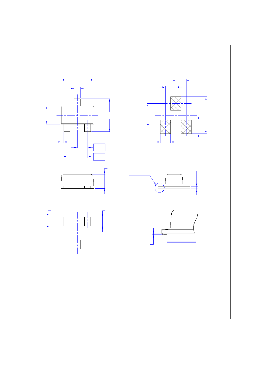
Dimensional Outline and Pad Layout
NOTES: UNLESS OTHERWISE SPECIFIED
A) THIS PACKAGE CONFORMS TO EIAJ
SC89 PACKAGING STANDARD.
B) ALL DIMENSIONS ARE IN MILLIMETERS.
C) DIMENSIONS ARE EXCLUSIVE OF BURRS,
MOLD FLASH, AND TIE BAR EXTRUSIONS.
1.70
1.50
0.98
0.78
1.70
1.50
0.50
1.00
0.35
0.25
0.54
0.34
0.43
0.28
0.78
0.58
(0.15)
1
2
3
LAND PATTERN RECOMMENDATION
1.80
0.50
1.14
0.50
0.50
0.66
SEE DETAIL A
0.20
0.04
DETAIL A
SCALE 2 : 1
0.10
0.00
F
D
Y
3
0
0
N
Z
S
i
n
g
l
e
N
-
C
h
a
n
n
e
l
2
.
5
V
S
p
e
c
i
f
i
e
d
P
o
w
e
r
T
r
e
n
c
h
®
®
®
®
M
O
S
F
E
T