 | ÐлекÑÑоннÑй компоненÑ: FDZ2554P | СкаÑаÑÑ:  PDF PDF  ZIP ZIP |
Äîêóìåíòàöèÿ è îïèñàíèÿ www.docs.chipfind.ru
August 2004
©
2004 Fairchild Semiconductor Corporation
FDZ2554P Rev C5 (W)
FDZ2554P
Monolithic Common Drain P-Channel 2.5V Specified PowerTrench
®
®
®
®
BGA MOSFET
General Description
Combining Fairchild's advanced 2.5V specified
PowerTrench process with state-of-the-art BGA
packaging, the FDZ2554P minimizes both PCB space
and R
DS(ON)
. This monolithic common drain BGA
MOSFET embodies a breakthrough in packaging
technology which enables the device to combine
excellent thermal transfer characteristics, high current
handling capability, ultra-low profile packaging, low gate
charge, and low R
DS(ON)
.
Applications
·
Battery management
·
Load switch
·
Battery protection
Features
·
6.5 A, 20 V. R
DS(ON)
= 28 m
@ V
GS
= 4.5 V
R
DS(ON)
= 45 m
@ V
GS
= 2.5 V
·
Occupies only 0.10 cm
2
of PCB area:
1/3 the area of SO-8
·
Ultra-thin package: less than 0.80 mm height when
mounted to PCB
·
Outstanding thermal transfer characteristics:
significantly better than SO-8
·
Ultra-low Q
g
x R
DS(ON)
figure-of-merit
·
High power and current handling capability
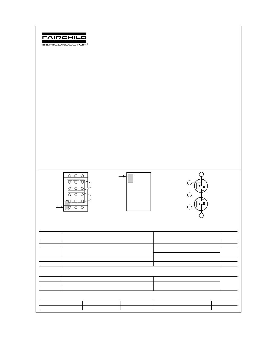
Q2
Q1
Pin 1
G
S
D
D
S
S
S
D
S
S
S
S
G
S
S
D
D
D
Bottom
Pin 1
F
2
5
5
4
Top
S
S
G
G
D
Q1
Q2
Absolute Maximum Ratings
T
A
=25
o
C unless otherwise noted
Symbol
Parameter
Ratings
Units
V
DSS
Drain-Source Voltage
20
V
V
GSS
Gate-Source Voltage
±
12
V
I
D
Drain Current Continuous
(Note 1a)
6.5
A
Pulsed
20
P
D
Power Dissipation (Steady State)
(Note 1a)
2.1
W
T
J
, T
STG
Operating and Storage Junction Temperature Range
55 to +150
°
C
Thermal Characteristics
R
JA
Thermal Resistance, Junction-to-Ambient
(Note 1a)
60
°
C/W
R
JB
Thermal Resistance, Junction-to-Ball
(Note 1b)
6.3
R
JC
Thermal Resistance, Junction-to-Case
(Note 1)
0.6
Package Marking and Ordering Information
Device Marking
Device
Reel Size
Tape width
Quantity
2554P
FDZ2554P
7''
12mm
3000 units
F
D
Z
2
5
5
4
P
FDZ2554P Rev C5 (W)
Electrical Characteristics
T
A
= 25°C unless otherwise noted
Symbol
Parameter
Test Conditions
Min Typ Max Units
Off Characteristics
BV
DSS
DrainSource Breakdown Voltage V
GS
= 0 V, I
D
= 250
µ
A
20
V
BV
DSS
T
J
Breakdown Voltage Temperature
Coefficient
I
D
= 250
µ
A, Referenced to 25
°
C
13
mV/
°
C
I
DSS
Zero Gate Voltage Drain Current
V
DS
= 16 V, V
GS
= 0 V
1
µ
A
I
GSS
GateBody Leakage
V
GS
=
±
12 V, V
DS
= 0 V
±
100
nA
On Characteristics
(Note 2)
V
GS(th)
Gate Threshold Voltage
V
DS
= V
GS
, I
D
= 250
µ
A
0.6 0.8
1.5
V
V
GS(th)
T
J
Gate Threshold Voltage
Temperature Coefficient
I
D
= 250
µ
A, Referenced to 25
°
C
3
mV/
°
C
R
DS(on)
Static DrainSource
OnResistance
V
GS
= 4.5 V, I
D
= 6.5 A
V
GS
= 2.5 V, I
D
= 5 A
V
GS
= 4.5 V, I
D
= 6.5 A, T
J
=125
°
C
21
36
30
28
45
43
m
g
FS
Forward Transconductance
V
DS
= 5 V,
I
D
= 6.5 A
24
S
Dynamic Characteristics
C
iss
Input Capacitance
1430
pF
C
oss
Output Capacitance
319
pF
C
rss
Reverse Transfer Capacitance
V
DS
= 10 V,
V
GS
= 0 V,
f = 1.0 MHz
164
pF
R
G
Gate Resistance
V
GS
= 15 mV, f = 1.0 MHz
9.2
Switching Characteristics
(Note 2)
t
d(on)
TurnOn Delay Time
12
22
ns
t
r
TurnOn Rise Time
9
18
ns
t
d(off)
TurnOff Delay Time
62
100
ns
t
f
TurnOff Fall Time
V
DD
= 10 V,
I
D
= 1 A,
V
GS
= 4.5 V,
R
GEN
= 6
37
60
ns
Q
g
Total Gate Charge
14
20
nC
Q
gs
GateSource Charge
3
nC
Q
gd
GateDrain Charge
V
DS
= 10 V,
I
D
= 6.5 A,
V
GS
= 4.5 V
4
nC
DrainSource Diode Characteristics and Maximum Ratings
I
S
Maximum Continuous DrainSource Diode Forward Current
1.75
A
V
SD
DrainSource Diode Forward
Voltage
V
GS
= 0 V, I
S
= 1.75 A
(Note 2)
0.7
1.2
V
t
rr
Reverse Recovery Time
25
ns
Q
rr
Reverse Recovery Charge
I
F
= 6.5 A,
d
iF
/d
t
= 100 A/µs
20
nC
Notes:
1.
R
JA
is determined with the device mounted on a 1 in² 2 oz. copper pad on a 1.5 x 1.5 in. board of FR-4 material. The thermal resistance from the
junction to the circuit board side of the solder ball, R
JB
, is defined for reference. For R
JC
, the thermal reference point for the case is defined as the
top surface of the copper chip carrier. R
JC
and R
JB
are guaranteed by design while R
JA
is determined by the user's board design.
a)
60°C/W when mounted
on a 1in
2
pad of 2 oz
copper
b)
108°C/W when mounted
on a minimum pad of 2 oz
copper
Scale 1 : 1 on letter size paper
2.
Pulse Test: Pulse Width < 300
µ
s, Duty Cycle < 2.0%
F
D
Z
2
5
5
4
P
FDZ2554P Rev C5 (W)
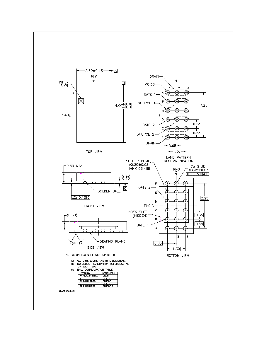
Dimensional Outline and Pad Layout
F
D
Z
2
5
5
4
P
F
D
Z
2
5
5
4
P
FDZ2554P Rev C5 (W)
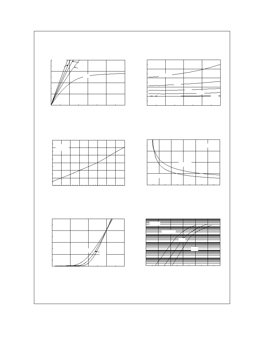
Typical Characteristics
0
5
10
15
20
0
0.5
1
1.5
2
-V
DS
, DRAIN-SOURCE VOLTAGE (V)
-
I
D
,
D
R
A
I
N
C
U
R
R
E
N
T
(
A
)
-3.0V
-3.5V
-2.5V
-2.0V
V
GS
= - 4.5V
0.8
1
1.2
1.4
1.6
1.8
0
5
10
15
20
-I
D
, DRAIN CURRENT (A)
R
D
S
(
O
N
)
,
N
O
R
M
A
L
I
Z
E
D
D
R
A
I
N
-
S
O
U
R
C
E
O
N
-
R
E
S
I
S
T
A
N
C
E
V
GS
= -2.5V
-4.0V
-3.5V
-4.5V
-3.0V
Figure 1. On-Region Characteristics.
Figure 2. On-Resistance Variation with
Drain Current and Gate Voltage.
0.8
0.9
1
1.1
1.2
1.3
1.4
-50
-25
0
25
50
75
100
125
150
T
J
, JUNCTION TEMPERATURE (
o
C)
R
D
S
(
O
N
)
,
N
O
R
M
A
L
I
Z
E
D
D
R
A
I
N
-
S
O
U
R
C
E
O
N
-
R
E
S
I
S
T
A
N
C
E
I
D
= -6.5A
V
GS
= -4.5V
0.01
0.03
0.05
0.07
0.09
1.5
2
2.5
3
3.5
4
4.5
-V
GS
, GATE TO SOURCE VOLTAGE (V)
R
D
S
(
O
N
)
,
O
N
-
R
E
S
I
S
T
A
N
C
E
(
O
H
M
)
I
D
= -3.2A
T
A
= 125
o
C
T
A
= 25
o
C
Figure 3. On-Resistance Variation with
Temperature.
Figure 4. On-Resistance Variation with
Gate-to-Source Voltage.
0
5
10
15
20
0.5
1
1.5
2
2.5
-V
GS
, GATE TO SOURCE VOLTAGE (V)
-
I
D
,
D
R
A
I
N
C
U
R
R
E
N
T
(
A
)
T
A
= 125
o
C
25
o
C
-55
o
C
V
DS
= -5V
0.0001
0.001
0.01
0.1
1
10
100
0
0.2
0.4
0.6
0.8
1
1.2
-V
SD
, BODY DIODE FORWARD VOLTAGE (V)
-
I
S
,
R
E
V
E
R
S
E
D
R
A
I
N
C
U
R
R
E
N
T
(
A
)
T
A
= 125
o
C
25
o
C
-55
o
C
V
GS
= 0V
Figure 5. Transfer Characteristics.
Figure 6. Body Diode Forward Voltage Variation
with Source Current and Temperature.
F
D
Z
2
5
5
4
P
FDZ2554P Rev C5 (W)
Typical Characteristics
0
1
2
3
4
5
0
4
8
12
16
Q
g
, GATE CHARGE (nC)
-
V
G
S
,
G
A
T
E
-
S
O
U
R
C
E
V
O
L
T
A
G
E
(
V
)
I
D
= -6.5A
V
DS
= -5V
-15V
-10V
0
400
800
1200
1600
2000
0
5
10
15
20
-V
DS
, DRAIN TO SOURCE VOLTAGE (V)
C
A
P
A
C
I
T
A
N
C
E
(
p
F
)
C
iss
C
rss
C
oss
f = 1MHz
V
GS
= 0 V
Figure 7. Gate Charge Characteristics.
Figure 8. Capacitance Characteristics.
0.01
0.1
1
10
100
0.1
1
10
100
-V
DS
, DRAIN-SOURCE VOLTAGE (V)
-
I
D
,
D
R
A
I
N
C
U
R
R
E
N
T
(
A
)
DC
1s
100ms
R
DS(ON)
LIMIT
V
GS
= -4.5V
SINGLE PULSE
R
JA
= 108
o
C/W
T
A
= 25
o
C
10ms
1ms
10s
0
10
20
30
40
50
0.01
0.1
1
10
100
1000
t
1
, TIME (sec)
P
(
p
k
)
,
P
E
A
K
T
R
A
N
S
I
E
N
T
P
O
W
E
R
(
W
)
SINGLE PULSE
R
JA
= 108°C/W
T
A
= 25°C
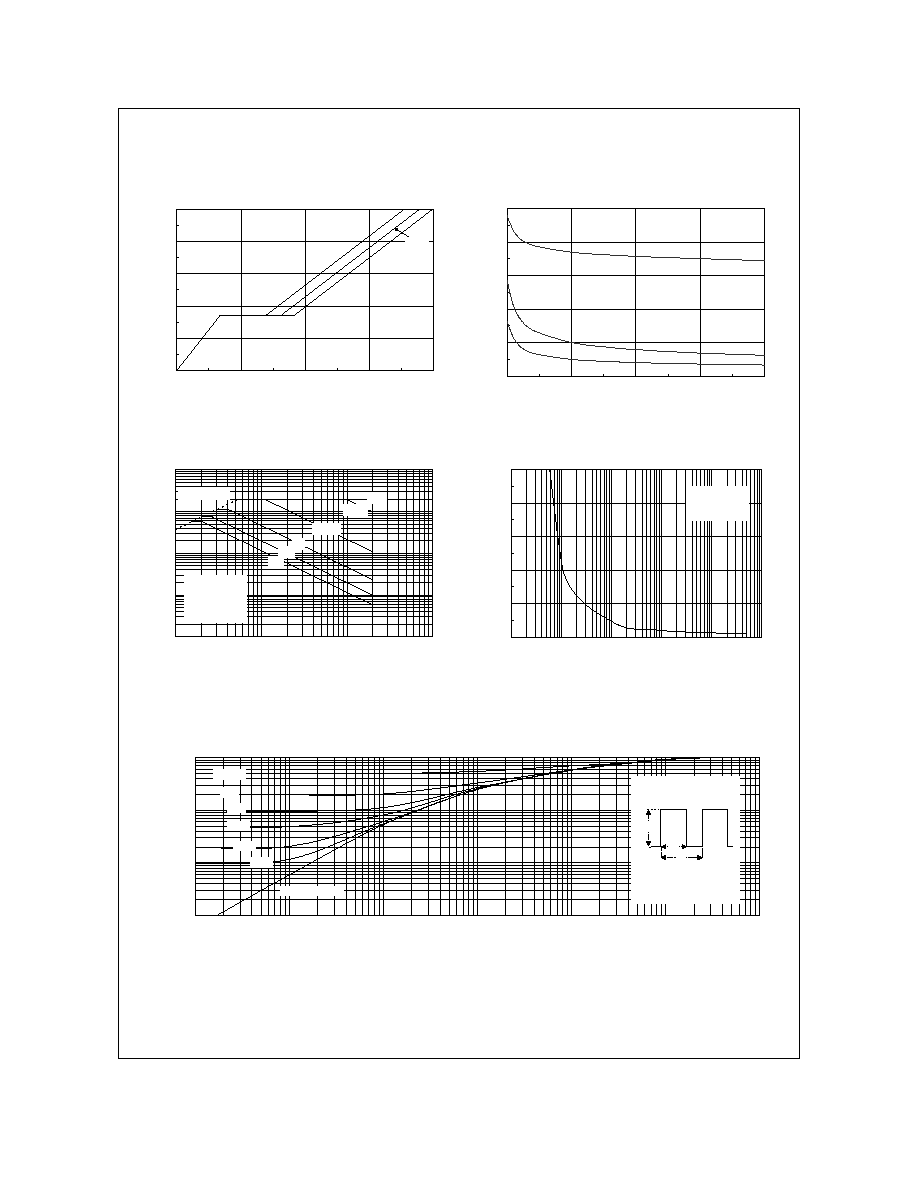
Figure 9. Maximum Safe Operating Area.
Figure 10. Single Pulse Maximum
Power Dissipation.
0.001
0.01
0.1
1
0.001
0.01
0.1
1
10
100
1000
t
1
, TIME (sec)
r
(
t
)
,
N
O
R
M
A
L
I
Z
E
D
E
F
F
E
C
T
I
V
E
T
R
A
N
S
I
E
N
T
T
H
E
R
M
A
L
R
E
S
I
S
T
A
N
C
E
R
JA
(t) = r(t) * R
JA
R
JA
= 108 °C/W
T
J
- T
A
= P * R
JA
(t)
Duty Cycle, D = t
1
/ t
2
P(pk)
t
1
t
2
SINGLE PULSE
0.01
0.02
0.05
0.1
0.2
D = 0.5
Figure 11. Transient Thermal Response Curve.
Thermal characterization performed using the conditions described in Note 1b.
Transient thermal response will change depending on the circuit board design.
F
D
Z
2
5
5
4
P