 | ÐлекÑÑоннÑй компоненÑ: FDZ294N | СкаÑаÑÑ:  PDF PDF  ZIP ZIP |
Äîêóìåíòàöèÿ è îïèñàíèÿ www.docs.chipfind.ru
July 2005
©
2005 Fairchild Semiconductor Corporation
FDZ294N Rev. B3 (W)
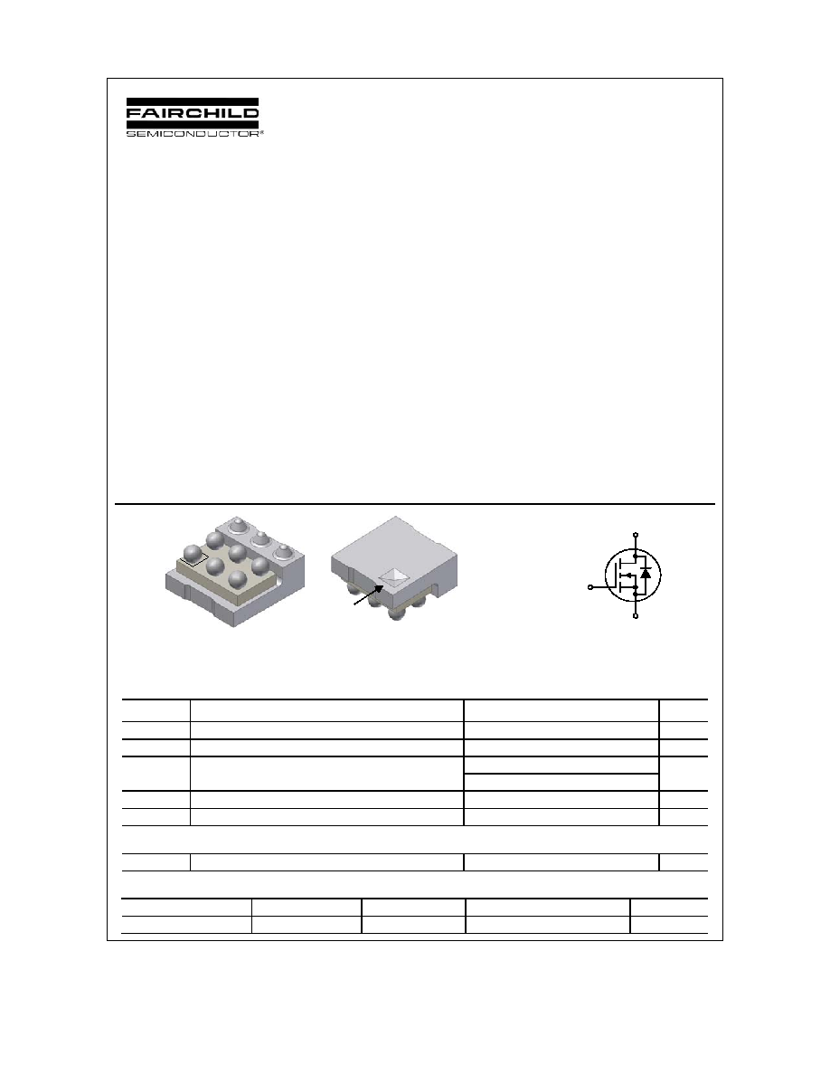
FDZ294N
N-Channel 2.5 V Specified PowerTrench
®
BGA MOSFET
General Description
Combining Fairchild's advanced 2.5V specified
PowerTrench process with state of the art BGA
packaging, the FDZ294N minimizes both PCB space
and R
DS(ON)
. This BGA MOSFET embodies a
breakthrough in packaging technology which enables
the device to combine excellent thermal transfer
characteristics, high current handling capability, ultra-
low profile packaging, low gate charge, and low R
DS(ON)
.
Applications
·
Battery management
·
Battery protection
Features
·
6 A, 20 V
R
DS(ON)
= 23 m
@ V
GS
= 4.5 V
R
DS(ON)
= 34 m
@ V
GS
= 2.5 V
·
Occupies only 2.25 mm
2
of PCB area.
Less than 50% of the area of a SSOT-6
·
Ultra-thin package: less than 0.85mm height when
mounted to PCB
·
Outstanding thermal transfer characteristics:
4 times better than SSOT-6
·
Ultra-low Q
g
x R
DS(ON)
figure-of-merit
·
High power and current handling capability.
GATE
Bottom
Top
S
G
D
Absolute Maximum Ratings
T
A
=25
o
C unless otherwise noted
Symbol Parameter
Ratings
Units
V
DSS
Drain-Source Voltage
20
V
V
GSS
Gate-Source
Voltage
±
12
V
I
D
Drain Current Continuous
(Note 1a)
6 A
Pulsed
10
P
D
Power Dissipation for Single Operation
(Note 1a)
1.7 W
T
J
, T
STG
Operating and Storage Junction Temperature Range
55 to +150
°
C
Thermal Characteristics
R
JA
Thermal Resistance, Junction-to-Ambient
(Note 1a)
72
°
C/W
Package Marking and Ordering Information
Device Marking
Device
Reel Size
Tape width
Quantity
E FDZ294N
7"
8mm
3000
units
FDZ294N
Index
slot
FDZ294N Rev. B3 (W)
FDZ294N
Electrical Characteristics
T
A
= 25°C unless otherwise noted
Symbol Parameter
Test
Conditions
Min Typ
Max
Units
Off Characteristics
BV
DSS
DrainSource Breakdown
Voltage
V
GS
= 0 V,
I
D
= 250
µ
A
20 V
BV
DSS
T
J
Breakdown Voltage Temperature
Coefficient
I
D
= 250
µ
A,Referenced to 25
°
C
12
mV/
°
C
I
DSS
Zero Gate Voltage Drain Current V
DS
= 16 V,
V
GS
= 0 V
1
µ
A
I
GSS
GateBody
Leakage.
V
GS
=
±
12 V,
V
DS
= 0 V
±
100
nA
On Characteristics
(Note 2)
V
GS(th)
Gate Threshold Voltage
V
DS
= V
GS
,
I
D
= 250
µ
A
0.6 0.9 1.5 V
V
GS(th)
T
J
Gate Threshold Voltage
Temperature Coefficient
I
D
= 250
µ
A,Referenced to 25
°
C
3 mV/
°
C
R
DS(on)
Static DrainSource
OnResistance
V
GS
= 4.5 V,
I
D
= 6 A,
V
GS
= 2.5 V,
I
D
= 5A,
V
GS
= 4.5 V, I
D
= 6 A, T
J
=125
°
C
18
26
24
23
34
31
m
g
FS
Forward
Transconductance
V
DS
= 5 V,
I
D
= 6 A
24
S
Dynamic Characteristics
C
iss
Input
Capacitance
670
pF
C
oss
Output
Capacitance
172
pF
C
rss
Reverse Transfer Capacitance
V
DS
= 10 V,
V
GS
= 0 V,
f = 1.0 MHz
105 pF
R
G
Gate
Resistance
V
GS
= 15 mV, f = 1.0 MHz
1.4
Switching Characteristics
(Note 2)
t
d(on)
TurnOn
Delay
Time
8
16
ns
t
r
TurnOn Rise Time
5
10
ns
t
d(off)
TurnOff Delay Time
14
25
ns
t
f
TurnOff
Fall
Time
V
DD
= 10 V,
I
D
= 1 A,
V
GS
= 4.5 V,
R
GEN
= 6
6 12 ns
Q
g
Total Gate Charge
7
10
nC
Q
gs
GateSource
Charge
1.4
nC
Q
gd
GateDrain
Charge
V
DS
= 10V,
I
D
= 6 A,
V
GS
= 4.5 V
2.1 nC
DrainSource Diode Characteristics and Maximum Ratings
I
S
Maximum Continuous DrainSource Diode Forward Current
1.4
A
V
SD
DrainSource Diode Forward
Voltage
V
GS
= 0 V, I
S
= 1.4 A
(Note 2)
0.7
1.2
V
t
rr
Diode Reverse Recovery Time
15
nS
Q
rr
Diode Reverse Recovery Charge
I
F
= 6 A,
d
iF
/d
t
= 100 A/µs
4 nC
Notes:
1.
R
JA
is determined with the device mounted on a 1 in² 2 oz. copper pad on a 1.5 x 1.5 in. board of FR-4 material. The thermal resistance from the junction to
the circuit board side of the solder ball, R
JB
, is defined for reference. For R
JC
, the thermal reference point for the case is defined as the top surface of the
copper chip carrier. R
JC
and R
JB
are guaranteed by design while R
JA
is determined by the user's board design.
a) 72°C/W
when
mounted on a 1in
2
pad
of 2 oz copper, 1.5" x
1.5" x 0.062" thick
PCB
b) 157°C/W
when
mounted
on a minimum pad of 2 oz
copper
2. Pulse Test: Pulse Width < 300
µ
s, Duty Cycle < 2.0%
FDZ294N Rev. B3 (W)
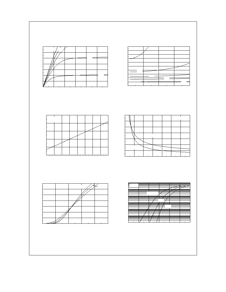
Typical Characteristics
0
5
10
15
20
25
30
35
0
0.5
1
1.5
2
2.5
3
V
DS
, DRAIN-SOURCE VOLTAGE (V)
I
D
,
DRA
I
N
CUR
RENT
(
A
)
2.5V
2.0V
3.5V
3.0V
V
GS
= 4.5V
0.8
1
1.2
1.4
1.6
1.8
2
2.2
2.4
2.6
2.8
0
5
10
15
20
I
D
, DRAIN CURRENT (A)
R
DS
(O
N
)
,
NO
R
M
AL
I
Z
E
D
DR
AI
N
-
S
O
UR
CE
O
N
-
R
ES
I
S
T
A
N
C
E
V
GS
= 2.0V
3.5V
3.0V
4.5V
2.5V
Figure 1. On-Region Characteristics.
Figure 2. On-Resistance Variation with
Drain Current and Gate Voltage.
0.6
0.8
1
1.2
1.4
1.6
-50
-25
0
25
50
75
100
125
150
T
J
, JUNCTION TEMPERATURE (
o
C)
R
DS
(O
N)
,
N
O
RM
AL
I
Z
E
D
D
RAI
N
-
SO
U
RCE
O
N
-
R
ES
IS
T
A
N
C
E
I
D
= 6A
V
GS
= 4.5V
0.01
0.02
0.03
0.04
0.05
0.06
0.07
0.08
1.5
2
2.5
3
3.5
4
4.5
5
V
GS
, GATE TO SOURCE VOLTAGE (V)
R
DS
(O
N)
,
ON-
R
ESI
ST
ANCE (
O
HM
)
I
D
=3A
T
A
= 125
o
C
T
A
= 25
o
C
Figure 3. On-Resistance Variation with
Temperature.
Figure 4. On-Resistance Variation with
Gate-to-Source Voltage.
0
5
10
15
20
25
30
35
1
1.5
2
2.5
3
3.5
V
GS
, GATE TO SOURCE VOLTAGE (V)
I
D
,
DR
AI
N C
U
R
R
E
N
T
(A
)
T
A
= -55
o
C
25
o
C
125
o
C
V
DS
= 5V
0.0001
0.001
0.01
0.1
1
10
100
0
0.2
0.4
0.6
0.8
1
1.2
V
SD
, BODY DIODE FORWARD VOLTAGE (V)
I
S
,
RE
VE
RS
E D
RAI
N
CU
RRE
NT
(
A
)
T
A
= 125
o
C
25
o
C
-55
o
C
V
GS
= 0V
Figure 5. Transfer Characteristics.
Figure 6. Body Diode Forward Voltage Variation
with Source Current and Temperature.
FDZ294N
FDZ294N Rev. B3 (W)
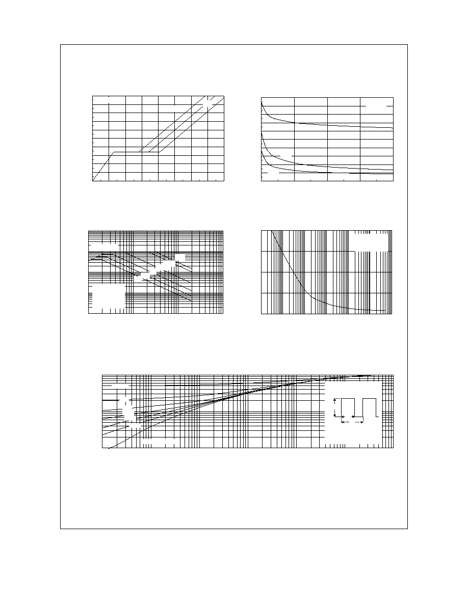
Typical Characteristics
0
0.5
1
1.5
2
2.5
3
3.5
4
4.5
5
0
1
2
3
4
5
6
7
8
Q
g
, GATE CHARGE (nC)
V
GS
,
GAT
E-SOUR
CE VOLT
AGE (V)
I
D
= 6A
V
DS
= 5V
15V
10V
0
100
200
300
400
500
600
700
800
900
1000
0
5
10
15
20
V
DS
, DRAIN TO SOURCE VOLTAGE (V)
C
A
P
A
C
I
TA
NC
E (
pF)
C
ISS
C
RSS
C
OSS
f = 1MHz
V
GS
= 0 V
Figure 7. Gate Charge Characteristics.
Figure 8. Capacitance Characteristics.
0.01
0.1
1
10
100
0.1
1
10
100
V
DS
, DRAIN-SOURCE VOLTAGE (V)
I
D
,
DR
AI
N C
U
R
R
E
N
T
(A
)
DC
10s
1s
100ms
R
DS(ON)
LIMIT
V
GS
= 4.5V
SINGLE PULSE
R
JA
= 157
o
C/W
T
A
= 25
o
C
10ms
1ms
0
5
10
15
20
0.001
0.01
0.1
1
10
100
1000
t
1
, TIME (sec)
P
(
p
k
)
,
PEAK T
RANSI
E
NT
PO
W
E
R
(
W
)
SINGLE PULSE
R
JA
= 157°C/W
T
A
= 25°C
Figure 9. Maximum Safe Operating Area.
Figure 10. Single Pulse Maximum
Power Dissipation.
0.01
0.1
1
0.001
0.01
0.1
1
10
100
1000
t
1
, TIME (sec)
r
(t),
N
O
R
M
A
L
I
Z
E
D
E
F
F
E
C
T
I
V
E
T
R
A
N
S
I
E
N
T
T
H
E
R
MA
L
RE
S
I
S
T
ANC
E
R
JA
(t) = r(t) * R
JA
R
JA
= 157 °C/W
T
J
- T
A
= P * R
JA
(t)
Duty Cycle, D = t
1
/ t
2
P(pk)
t
1
t
2
SINGLE PULSE
0.01
0.02
0.05
0.1
0.2
D = 0.5
Figure 11. Transient Thermal Response Curve.
Thermal characterization performed using the conditions described in Note 1b.
Transient thermal response will change depending on the circuit board design.
FDZ294N
FDZ294N Rev. B3 (W)
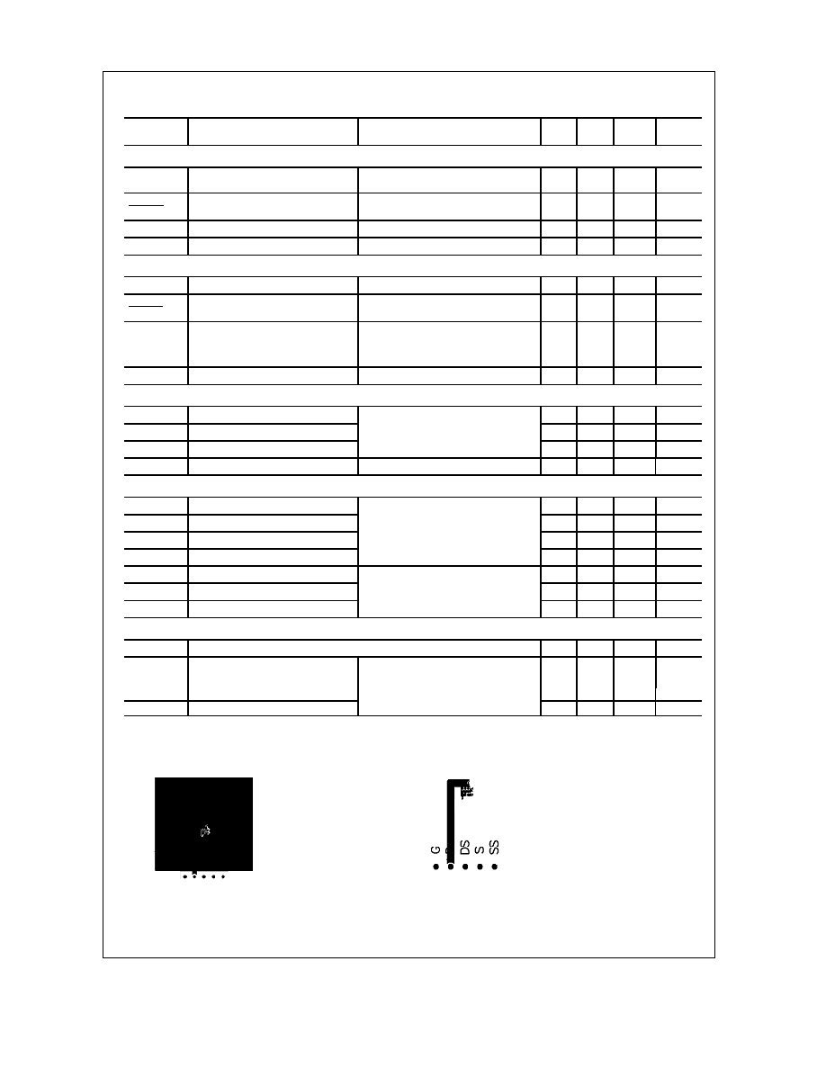
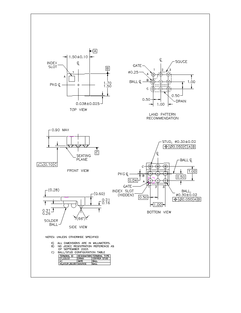
Dimensional Outline and Pad Layout
FDZ294N