 | ÐлекÑÑоннÑй компоненÑ: FDZ5047N | СкаÑаÑÑ:  PDF PDF  ZIP ZIP |
Äîêóìåíòàöèÿ è îïèñàíèÿ www.docs.chipfind.ru
January 2004
2004 Fairchild Semiconductor Corporation.
FDZ5047N Rev D4 (W)
FDZ5047N
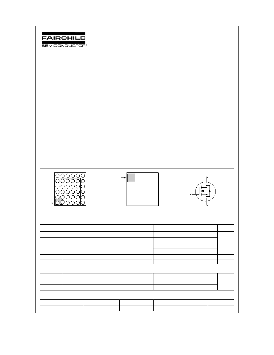
30V N-Channel Logic Level PowerTrench
BGA MOSFET
General Description
Combining Fairchild's 30V PowerTrench process with
state of the art BGA packaging, the FDZ5047N
minimizes both PCB space and R
DS(ON)
. This BGA
MOSFET embodies a breakthrough in packaging
technology which enables the device to combine
excellent thermal transfer characteristics, high current
handling capability, ultra-low profile packaging, low gate
charge, and low R
DS(ON)
.
These MOSFETs feature faster switching and lower
gate charge than other MOSFETs with comparable
R
DS(ON)
specifications resulting in DC/DC power supply
designs with higher overall efficiency.
Applications
· DC/DC converters
· Solenoid drive
Features
· 22 A, 30 V.
R
DS(ON)
= 2.9 m
@ V
GS
= 10 V
R
DS(ON)
= 4.5 m
@ V
GS
= 4.5 V
· Occupies only 27.5 mm
2
of PCB area:
1/5 of the area of a TO-220 package
· Ultra-thin package: less than 0.90 mm height when
mounted to PCB
· Outstanding thermal transfer characteristics
· Ultra-low gate charge x R
DS(ON)
product
Pin 1
D
D
D
D
D
D
D
D
D
D
D
D
D
D
S
S
S
S
S
G
S
S
S
S
D
S
S
S
S
S
D
S
S
S
S
S
Bottom
F
5
047
Pin 1
Top
S
D
G
Absolute Maximum Ratings
T
A
=25
o
C unless otherwise noted
Symbol Parameter
Ratings
Units
V
DSS
Drain-Source Voltage
30
V
V
GSS
Gate-Source
Voltage
±20
I
D
Drain Current Continuous
(Note 1a)
22 A
Pulsed
75
P
D
Total Power Dissipation @ T
A
= 25
°C
2.8 W
T
J
, T
STG
Operating and Storage Junction Temperature Range
50 to +150
°C
Thermal Characteristics
R
JA
Thermal Resistance, Junction-to-Ambient
(Note 1a)
44
°C/W
R
JB
Thermal Resistance, Junction-to-Ball
(Note 1)
2.7
R
JC
Thermal Resistance, Junction-to-Case
(Note 1)
0.3
Package Marking and Ordering Information
Device Marking
Device
Reel Size
Tape width
Quantity
5047N
FDZ5047N
13''
12mm
3000 units
FDZ5047N
FDZ5047N Rev D4 (W)
Electrical Characteristics
T
A
= 25°C unless otherwise noted
Symbol Parameter
Test
Conditions
Min
Typ
Max
Units
Off Characteristics
BV
DSS
DrainSource Breakdown Voltage V
GS
= 0 V,
I
D
= 250
µA
30 V
BV
DSS
T
J
Breakdown Voltage Temperature
Coefficient
I
D
= 250
µA, Referenced to 25°C
24
mV/
°C
I
DSS
Zero Gate Voltage Drain Current
V
DS
= 24 V,
V
GS
= 0 V
1
µA
I
GSSF
GateBody Forward Leakage
V
GS
= 20 V,
V
DS
= 0 V
100
nA
I
GSSR
GateBody Reverse Leakage
V
GS
= 20 V, V
DS
= 0 V
100
nA
On Characteristics
(Note 2)
V
GS(th)
Gate Threshold Voltage
V
DS
= V
GS
,
I
D
= 250
µA
1 1.3 3 V
V
GS(th)
T
J
Gate Threshold Voltage
Temperature Coefficient
I
D
= 250
µA, Referenced to 25°C
5
mV/
°C
R
DS(on)
Static DrainSource
OnResistance
V
GS
= 10 V,
I
D
= 22 A
V
GS
= 4.5 V, I
D
= 18 A
V
GS
= 10 V, I
D
= 22 A, T
A
=125
°C
2.3
3.2
3.4
2.9
4.5
5.0
m
g
FS
Forward
Transconductance V
DS
= 10 V,
I
D
= 22 A
100
S
Dynamic Characteristics
C
iss
Input
Capacitance
4993
pF
C
oss
Output
Capacitance
1144
pF
C
rss
Reverse Transfer Capacitance
V
DS
= 15 V,
V
GS
= 0 V,
f = 1.0 MHz
498 pF
Switching Characteristics
(Note 2)
t
d(on)
TurnOn
Delay
Time
11
20
ns
t
r
TurnOn Rise Time
12
22
ns
t
d(off)
TurnOff Delay Time
119
190
ns
t
f
TurnOff
Fall
Time
V
DD
= 15 V,
I
D
= 1 A,
V
GS
= 10 V,
R
GEN
= 6
55
88 ns
Q
g
Total Gate Charge
52
73
nC
Q
gs
GateSource
Charge
11
nC
Q
gd
GateDrain
Charge
V
DS
= 15 V,
I
D
= 22 A,
V
GS
= 5 V
17 nC
DrainSource Diode Characteristics and Maximum Ratings
I
S
Maximum Continuous DrainSource Diode Forward Current
(Note 1a)
2.3
A
V
SD
DrainSource
Diode
Forward
Voltage
V
GS
= 0 V, I
S
= 2.3 A
(Note 2)
0.7
1.2 V
t
rr
Diode Reverse Recovery Time
42
nS
Q
rr
Diode Reverse Recovery Charge
I
F
= 22A,
d
iF
/d
t
= 100 A/µs
59 nC
·
Notes:
1. R
JA
is determined with the device mounted on a 1 in² 2 oz. copper pad on a 1.5 x 1.5 in. board of FR-4 material. The thermal resistance from the junction to the
circuit board side of the solder ball, R
JB
, is defined for reference. For R
JC
, the thermal reference point for the case is defined as the top surface of the copper
chip carrier. R
JC
and R
JB
are guaranteed by design while R
JA
is determined by the user's board design.
a)
44°C/W when mounted
on a 1in
2
pad of 2 oz
copper
b)
95°C/W when mounted on
a minimum pad of 2 oz
copper
Scale 1 : 1 on letter size paper
2. Pulse Test: Pulse Width < 300
µs, Duty Cycle < 2.0%
FDZ5047N
FDZ5047N Rev D4 (W)
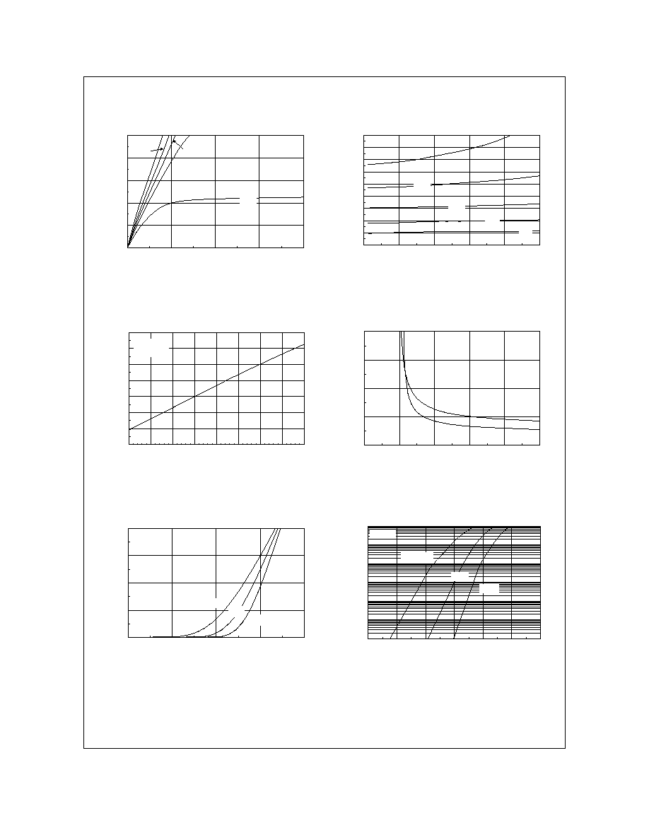
Typical Characteristics
0
20
40
60
80
100
0
0.5
1
1.5
2
V
DS
, DRAIN-SOURCE VOLTAGE (V)
I
D
, DRAIN CURRENT (A)
2.5V
3.0V
3.5V
4.5V
V
GS
=10V
0.8
1
1.2
1.4
1.6
1.8
2
2.2
2.4
2.6
0
20
40
60
80
100
I
D
, DRAIN CURRENT (A)
R
DS
(O
N)
, NORMALIZED
DRAIN-SOURCE ON-RESISTANCE
V
GS
= 3.0V
6.0V
3.5V
10V
4.5V
Figure 1. On-Region Characteristics.
Figure 2. On-Resistance Variation with
Drain Current and Gate Voltage.
0.4
0.6
0.8
1
1.2
1.4
1.6
1.8
-50
-25
0
25
50
75
100
125
150
T
J
, JUNCTION TEMPERATURE (
o
C)
R
DS(O
N)
, NORMALIZED
DRAIN-SOURCE ON-RESISTANCE
I
D
= 22A
V
GS
= 10V
0.000
0.004
0.008
0.012
0.016
0
2
4
6
8
10
V
GS
, GATE TO SOURCE VOLTAGE (V)
R
DS(
O
N)
, ON-RESISTANCE (OHM)
I
D
= 11 A
T
A
= 125
o
C
T
A
= 25
o
C
Figure 3. On-Resistance Variation with
Temperature.
Figure 4. On-Resistance Variation with
Gate-to-Source Voltage.
0
20
40
60
80
1
1.5
2
2.5
3
V
GS
, GATE TO SOURCE VOLTAGE (V)
I
D
, DRAIN CURRENT
(
A
)
T
A
= 125
o
C
25
o
C
-55
o
C
V
DS
= 10V
0.0001
0.001
0.01
0.1
1
10
100
0
0.2
0.4
0.6
0.8
1
1.2
V
SD
, BODY DIODE FORWARD VOLTAGE (V)
I
S
, REVERSE DRAIN CURRENT (A)
T
A
= 125
o
C
25
o
C
-55
o
C
V
GS
= 0V
Figure 5. Transfer Characteristics.
Figure 6. Body Diode Forward Voltage Variation
with Source Current and Temperature.
FDZ5047N
FDZ5047N Rev D4 (W)
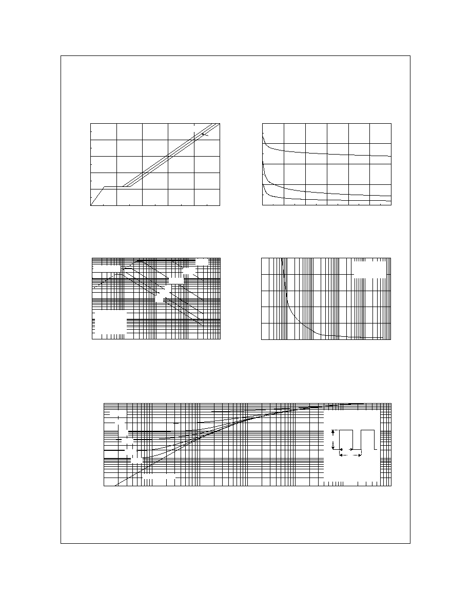
Typical Characteristics
0
2
4
6
8
10
0
20
40
60
80
100
Q
g
, GATE CHARGE (nC)
V
GS
, GATE-
S
OURCE VOLTAGE (
V
)
I
D
= 22A
V
DS
=10V
20V
15V
0
2000
4000
6000
8000
0
5
10
15
20
25
30
V
DS
, DRAIN TO SOURCE VOLTAGE (V)
CAPACITANCE (pF)
C
ISS
C
RSS
C
OSS
f =1MHz
V
GS
= 0V
Figure 7. Gate Charge Characteristics.
Figure 8. Capacitance Characteristics.
0.01
0.1
1
10
100
0.01
0.1
1
10
100
V
DS
, DRAIN-SOURCE VOLTAGE (V)
I
D
, DRAIN CURRENT (A)
DC
10s
1s
100ms
R
DS(ON)
LIMIT
V
GS
= 10V
SINGLE PULSE
R
JA
= 95
o
C/W
T
A
= 25
o
C
10ms
1ms
0
10
20
30
40
50
0.01
0.1
1
10
100
1000
t
1
, TIME (sec)
P(
pk)
,
PEAK TRANSIENT POWER (
W
)
SINGLE PULSE
R
JA
= 95°C/W
T
A
= 25°C
Figure 9. Maximum Safe Operating Area.
Figure 10. Single Pulse Maximum
Power Dissipation.
0.001
0.01
0.1
1
0.001
0.01
0.1
1
10
100
1000
t
1
, TIME (sec)
r(t), NORM
ALIZED EFFECTIVE TRANSIENT
THERM
A
L RESISTANCE
R
JA
(t) = r(t) * R
JA
R
JA
= 95 °C/W
T
J
- T
A
= P * R
JA
(t)
Duty Cycle, D = t
1
/ t
2
P(pk)
t
1
t
2
SINGLE PULSE
0.01
0.02
0.05
0.1
0.2
D = 0.5
Figure 11. Transient Thermal Response Curve.
Thermal characterization performed using the conditions described in Note 1b.
Transient thermal response will change depending on the circuit board design.
FDZ5047N
FDZ5047N Rev D4 (W)
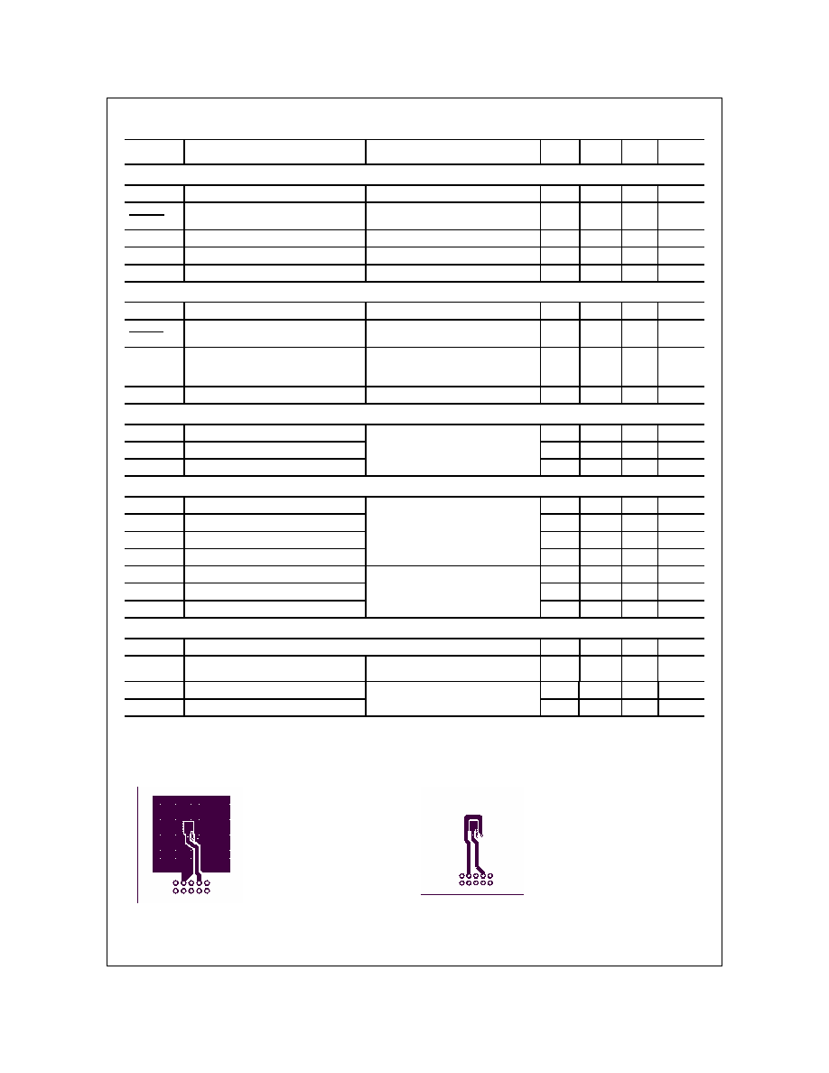
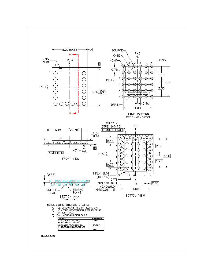
Dimensional Outline and Pad Layout
FDZ5047N