Äîêóìåíòàöèÿ è îïèñàíèÿ www.docs.chipfind.ru
tm
©2006 Fairchild Semiconductor Corporation
1
www.fairchildsemi.com
FGA15N120ANTD Rev. A
F
G
A15N120ANTD 1200V NPT T
r
ench IGBT
May 2006
FGA15N120ANTD
1200V NPT Trench IGBT
Features
· NPT Trench Technology, Positive temperature coefficient
· Low saturation voltage: V
CE(sat), typ
= 1.9V
@ I
C
= 15A and T
C
= 25
°C
· Low switching loss: E
off, typ
= 0.6mJ
@ I
C
= 15A and T
C
= 25
°C
· Extremely enhanced avalanche capability
Description
Using Fairchild's proprietary trench design and advanced NPT
technology, the 1200V NPT IGBT offers superior conduction
and switching performances, high avalanche ruggedness and
easy parallel operation.
This device is well suited for the resonant or soft switching appli-
cation such as induction heating, microwave oven, etc.
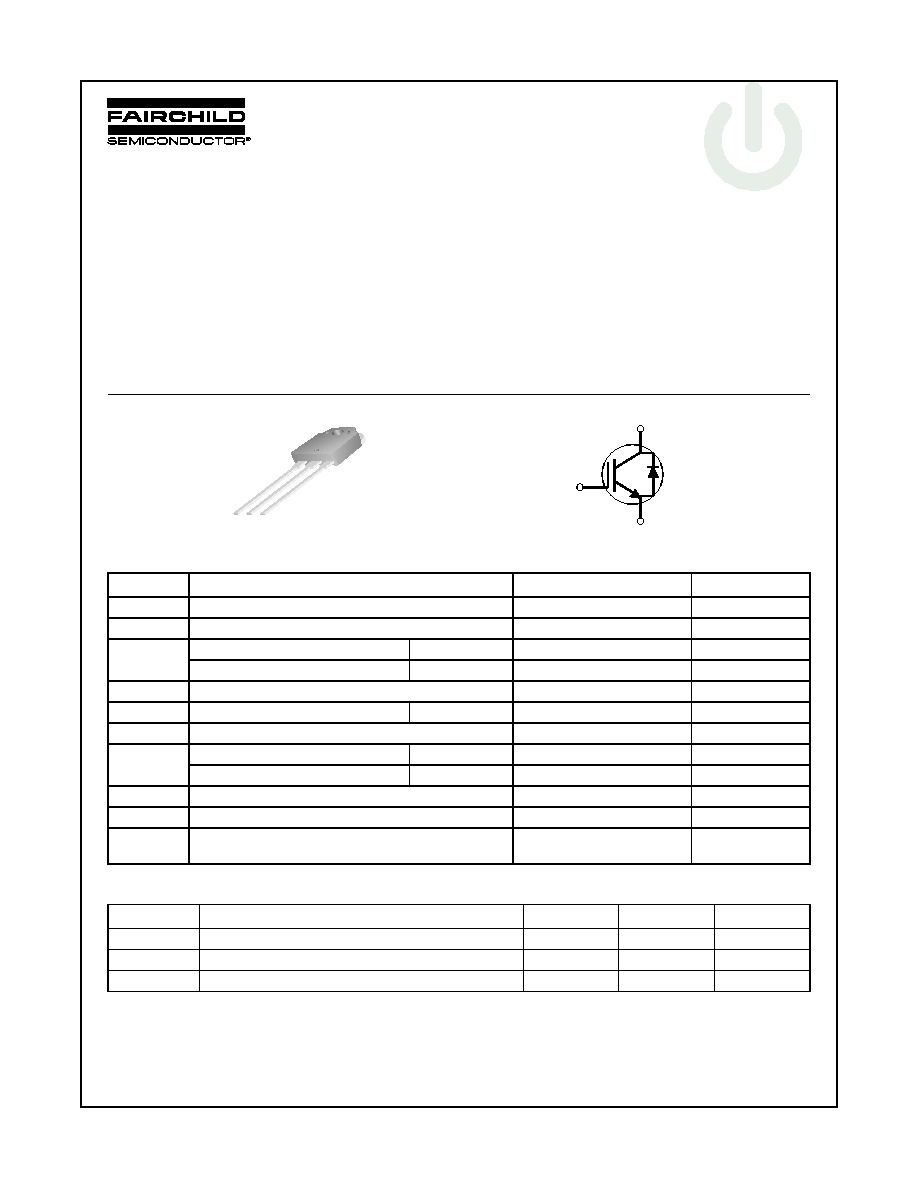
G
C
E
G
C
E
G C E
TO-3P
Absolute Maximum Ratings
Symbol
Description
FGA15N120ANTD
Units
V
CES
Collector-Emitter Voltage
1200
V
V
GES
Gate-Emitter Voltage
± 20
V
I
C
Collector Current
@ T
C
= 25
°C
30
A
Collector Current
@ T
C
= 100
°C
15
A
I
CM
Pulsed Collector Current
(Note 1)
45
A
I
F
Diode Continuous Forward Current
@ T
C
= 100
°C
15
A
I
FM
Diode Maximum Forward Current
45
A
P
D
Maximum Power Dissipation
@ T
C
= 25
°C
186
W
Maximum Power Dissipation
@ T
C
= 100
°C
74
W
T
J
Operating Junction Temperature
-55 to +150
°C
T
stg
Storage Temperature Range
-55 to +150
°C
T
L
Maximum Lead Temp. for soldering
Purposes, 1/8" from case for 5 seconds
300
°C
Thermal Characteristics
Symbol
Parameter
Typ.
Max.
Units
R
JC
Thermal Resistance, Junction-to-Case for IGBT
--
0.67
°C/W
R
JC
Thermal Resistance, Junction-to-Case for Diode
--
2.88
°C/W
R
JA
Thermal Resistance, Junction-to-Ambient
--
40
°C/W
Notes:
(1) Repetitive rating: Pulse width limited by max. junction temperature
2
www.fairchildsemi.com
FGA15N120ANTD Rev. A
F
G
A15N120ANTD 1200V NPT T
r
ench IGBT
Package Marking and Ordering Information
Device Marking
Device
Package
Reel Size
Tape Width
Quantity
FGA15N120ANTD
FGA15N120ANTD
TO-3P
--
--
30
Electrical Characteristics of the IGBT
T
C
= 25°C unless otherwise noted
Symbol
Parameter
Test Conditions
Min.
Typ.
Max.
Units
Off Characteristics
I
CES
Collector Cut-Off Current
V
CE
= V
CES
, V
GE
= 0V
--
--
3
mA
I
GES
G-E Leakage Current
V
GE
= V
GES
, V
CE
= 0V
--
--
± 250
nA
On Characteristics
V
GE(th)
G-E Threshold Voltage
I
C
= 15mA, V
CE
= V
GE
4.5
6.5
8.5
V
V
CE(sat)
Collector to Emitter
Saturation Voltage
I
C
= 15A
,
V
GE
= 15V
--
1.9
2.4
V
I
C
= 15A
,
V
GE
= 15V,
T
C
= 125
°C
--
2.2
--
V
I
C
= 30A
,
V
GE
= 15V
--
2.3
--
V
Dynamic Characteristics
C
ies
Input Capacitance
V
CE
= 30V
,
V
GE
= 0V,
f = 1MHz
--
2650
--
pF
C
oes
Output Capacitance
--
143
--
pF
C
res
Reverse Transfer Capacitance
--
96
--
pF
Switching Characteristics
t
d(on)
Turn-On Delay Time
V
CC
= 600 V, I
C
= 15A,
R
G
= 10
, V
GE
= 15V,
Inductive Load, T
C
= 25
°C
--
15
--
ns
t
r
Rise Time
--
20
--
ns
t
d(off)
Turn-Off Delay Time
--
160
--
ns
t
f
Fall Time
--
100
180
ns
E
on
Turn-On Switching Loss
--
3
4.5
mJ
E
off
Turn-Off Switching Loss
--
0.6
0.9
mJ
E
ts
Total Switching Loss
--
3.6
5.4
mJ
t
d(on)
Turn-On Delay Time
V
CC
= 600 V, I
C
= 15A,
R
G
= 10
, V
GE
= 15V,
Inductive Load, T
C
= 125
°C
--
15
--
ns
t
r
Rise Time
--
20
--
ns
t
d(off)
Turn-Off Delay Time
--
170
--
ns
t
f
Fall Time
--
150
--
ns
E
on
Turn-On Switching Loss
--
3.2
4.8
mJ
E
off
Turn-Off Switching Loss
--
0.8
1.2
mJ
E
ts
Total Switching Loss
--
4.0
6.0
mJ
Q
g
Total Gate Charge
V
CE
= 600 V, I
C
= 15A,
V
GE
= 15V
--
120
180
nC
Q
ge
Gate-Emitter Charge
--
16
22
nC
Q
gc
Gate-Collector Charge
--
50
65
nC
3
www.fairchildsemi.com
FGA15N120ANTD Rev. A
F
G
A15N120ANTD 1200V NPT T
r
ench IGBT
Electrical Characteristics of DIODE
T
C
= 25°C unless otherwise noted
Symbol
Parameter
Test Conditions
Min.
Typ.
Max.
Units
V
FM
Diode Forward Voltage
I
F
= 15A
T
C
= 25
°C
--
1.7
2.7
V
T
C
= 125
°C
--
1.8
--
t
rr
Diode Reverse Recovery Time
I
F
= 15A
dI/dt = 200 A/
s
T
C
= 25
°C
--
210
330
ns
T
C
= 125
°C
--
280
--
I
rr
Diode Peak Reverse Recovery Cur-
rent
T
C
= 25
°C
--
27
40
A
T
C
= 125
°C
--
31
--
Q
rr
Diode Reverse Recovery Charge
T
C
= 25
°C
--
2835
6600
nC
T
C
= 125
°C
--
4340
--
4
www.fairchildsemi.com
FGA15N120ANTD Rev. A
F
G
A15N120ANTD 1200V NPT T
r
ench IGBT
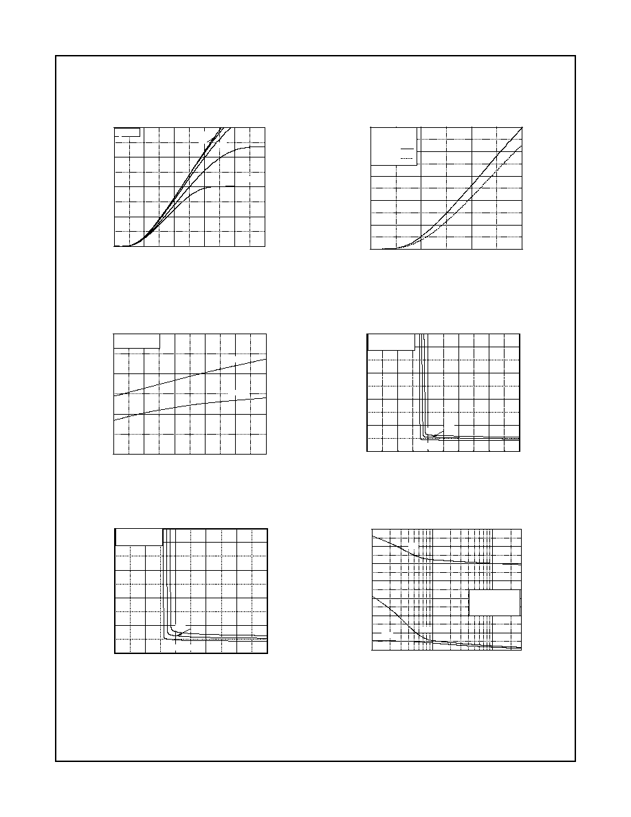
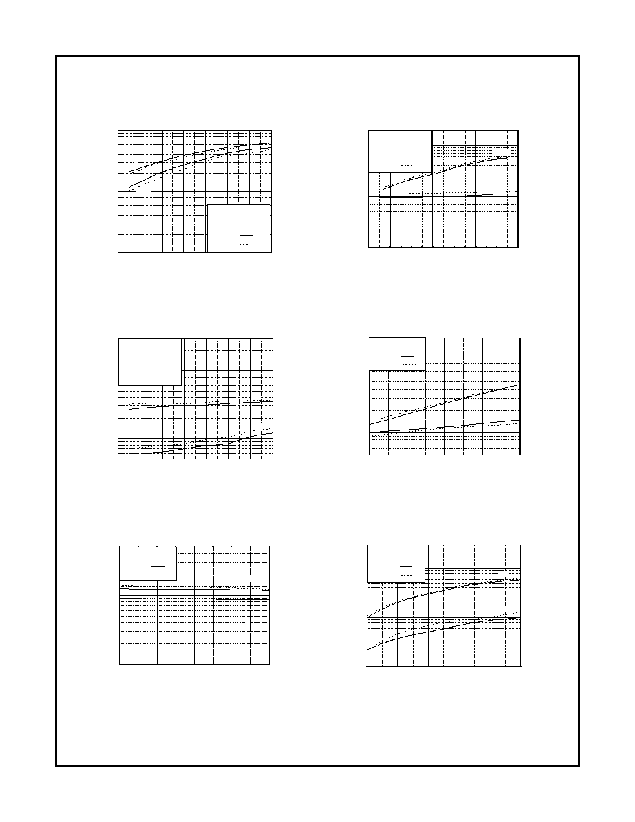
Typical Performance Characteristics
Figure 1. Typical Output Characteristics
Figure 2. Typical Saturation Voltage
0
2
4
6
8
10
0
50
100
150
200
T
C
= 25
o
C
20V
17V
15V
12V
V
GE
= 10V
Collector C
u
r
r
ent
, I
C
[A]
Collector-Emitter Voltage, V
CE
[V]
0
2
4
6
0
30
60
90
120
150
Common Emitter
V
GE
= 15V
T
C
= 25
o
C
T
C
= 125
o
C
Coll
e
c
tor
C
u
rrent ,
I
C
[A]
Collector-Emitter Voltage, V
CE
[V]
Characteristics
Figure 3. Saturation Voltage vs. Case
Figure 4. Saturation Voltage vs. V
GE
Temperature at Variant Current Level
25
50
75
100
125
150
1.5
2.0
2.5
3.0
Common Emitter
V
GE
= 15V
I
C
= 24A
I
C
= 15A
Collec
t
or-Emit
t
er Volt
age, V
CE
[V
]
Case Temperature, T
C
[
o
C]
0
4
8
12
16
20
0
4
8
12
16
24A
15A
Common Emitter
T
C
= 25
o
C
I
C
= 7.5A
Co
ll
ec
t
o
r-Em
i
tter V
o
l
t
a
g
e
,
V
CE
[V]
Gate-Emitter Voltage, V
GE
[V]
Figure 5. Saturation Voltage vs. V
GE
0.1
1
10
0
500
1000
1500
2000
2500
3000
3500
Ciss
Coss
Common Emitter
V
GE
= 0V, f = 1MHz
T
C
= 25
o
C
Crss
Ca
pacitanc
e [
p
F
]
Collector-Emitter Voltage, V
CE
[V]
0
4
8
12
16
20
0
4
8
12
16
24A
15A
Common Emitter
T
C
= 125
o
C
I
C
= 7.5A
Collect
o
r-E
mit
t
e
r Volt
age,
V
CE
[V]
Gate-Emitter Voltage, V
GE
[V]
Figure 6. Capacitance Characteristics
5
www.fairchildsemi.com
FGA15N120ANTD Rev. A
F
G
A15N120ANTD 1200V NPT T
r
ench IGBT
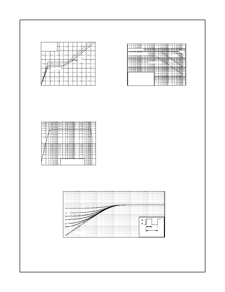
Typical Performance Characteristics
(Continued)
Figure 7. Turn-On Characteristics vs. Gate
Figure 8. Turn-Off Characteristics vs. Gate
Resistance
Resistance
0
10
20
30
40
50
60
70
1
10
100
Common Emitter
V
CC
= 600V, V
GE
= 15V
I
C
= 15A
T
C
= 25
o
C
T
C
= 125
o
C
td(on)
tr
Sw
it
c
hin
g Tim
e
[ns
]
Gate Resistance, R
G
[]
0
10
20
30
40
50
60
70
10
100
1000
Common Emitter
V
CC
= 600V, V
GE
= 15V
I
C
= 15A
T
C
= 25
o
C
T
C
= 125
o
C
td(off)
tf
S
w
itc
h
ing T
i
me [
n
s]
Gate Resistance, R
G
[
]
Figure 9. Switching Loss vs. Gate Resistance
Figure 10. Turn-On Characteristics vs.
0
10
20
30
40
50
60
70
1
10
Common Emitter
V
CC
= 600V, V
GE
= 15V
I
C
= 15A
T
C
= 25
o
C
T
C
= 125
o
C
Eon
Eoff
S
w
i
t
chin
g Lo
ss [mJ]
Gate Resistance, R
G
[]
10
15
20
25
30
10
100
Common Emitter
V
GE
= 15V, R
G
= 10
T
C
= 25
o
C
T
C
= 125
o
C
tr
td(on)
S
w
itc
h
ing T
im
e
[
n
s]
Collector Current, I
C
[A]
Collector Current
Figure 11. Turn-Off Characteristics vs.
Figure 12. Switching Loss vs. Collector Current
Collector Current
10
15
20
25
30
10
100
Common Emitter
V
GE
= 15V, R
G
= 10
T
C
= 25
o
C
T
C
= 125
o
C
td(off)
tf
Sw
i
t
ch
i
n
g
T
i
me
[ns
]
Collector Current, I
C
[A]
5
10
15
20
25
30
0.1
1
10
Common Emitter
V
GE
= 15V, R
G
= 10
T
C
= 25
o
C
T
C
= 125
o
C
Eon
Eoff
Sw
it
ch
ing Los
s
[
m
J]
Collector Current, I
C
[A]
6
www.fairchildsemi.com
FGA15N120ANTD Rev. A
F
G
A15N120ANTD 1200V NPT T
r
ench IGBT
Typical Performance Characteristics
(Continued)
Figure 13. Gate Charge Characteristics
Figure 14. SOA Characteristics
0
20
40
60
80
100
120
0
3
6
9
12
15
600V
400V
Common Emitter
R
L
= 40
T
C
= 25
o
C
Vcc = 200V
Gate-Em
it
ter Volt
a
ge,
V
GE
[V]
Gate Charge, Q
g
[nC]
0.1
1
10
100
1000
0.01
0.1
1
10
100
50
s
100
s
1m s
D C O peration
Ic M A X (P ulsed)
Ic M A X (C ontinuous)
S ingle N onrepetitive
P ulse T c = 25
o
C
C urves m ust be derated
linearly w ith increase
in tem perature
Co
l
l
e
c
to
r
Cu
r
r
e
n
t
, Ic
[
A
]
C ollector - E m itter V oltage, V
C E
[V ]
Figure 15. Turn-Off SOA
10
100
1000
1
10
100
Safe Operating Area
V
GE
= 15V, T
C
= 125
o
C
Collec
t
or Current
,
I
C
[A]
Collector-Emitter Voltage, V
CE
[V]
1E-5
1E-4
1E-3
0.01
0.1
1
10
1E-3
0.01
0.1
1
10
0.1
0.5
0.2
0.05
0.02
0.01
single pulse
Ther
ma
l Res
pon
se
[
Z
t
h
jc]
Rectangular Pulse Duration [sec]
Pdm
t1
t2
Duty factor D = t1 / t2
Peak Tj = Pdm
× Zthjc + T
C
Figure 16. Transient Thermal Impedance of IGBT
7
www.fairchildsemi.com
FGA15N120ANTD Rev. A
F
G
A15N120ANTD 1200V NPT T
r
ench IGBT
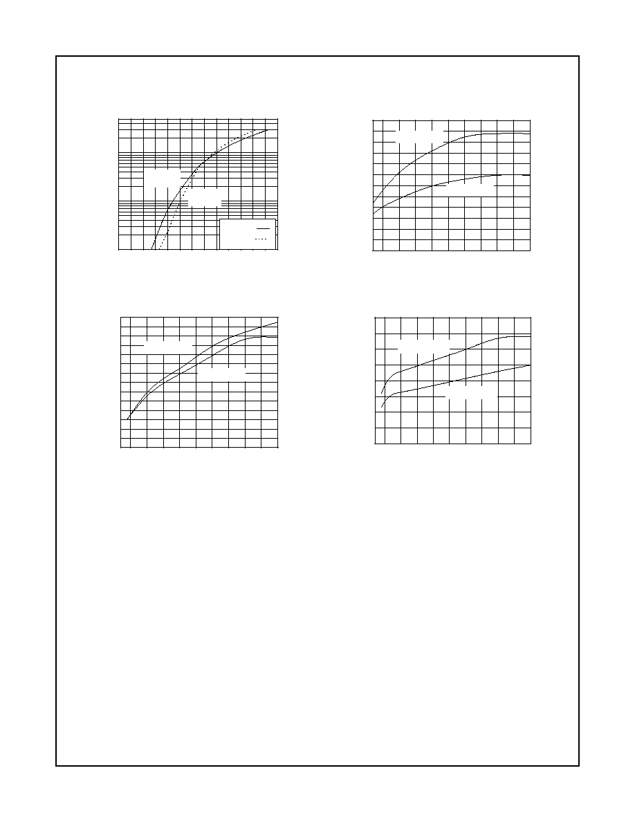
Typical Performance Characteristics
(Continued)
Figure 17. Forward Characteristics
Figure 18. Reverse Recovery Current
0.1
1
10
50
0.0
0.4
0.8
1.2
1.6
2.0
2.4
T
C
= 125
o
C
T
C
= 25
o
C
T
J
= 25
o
C
T
J
= 125
o
C
Forward Voltage , V
F
[V]
Fo
rwar
d Curr
ent , I
F
[A
]
5
10
15
20
25
0
5
10
15
20
25
30
di/dt = 100A/
s
di/dt = 200A/
s
Rever
s
e Recovery
Cur
r
net
,
I
rr
[A]
Forward Current , I
F
[A]
Figure 19. Stored Charge
Figure 20. Reverse Recovery Time
5
10
15
20
25
0
1000
2000
3000
4000
5000
6000
7000
di/dt = 100A/
s
di/dt = 200A/
s
St
or
ed Recover
y
Char
ge , Q
rr
[n
C
]
Forward Current , I
F
[A]
5
10
15
20
25
0
100
200
300
400
di/dt = 100A/
s
di/dt = 200A/
s
Reve
rse Re
cover
y
Tim
e
, t
rr
[n
s]
Forward Current , I
F
[A]
8
www.fairchildsemi.com
FGA15N120ANTD Rev. A
F
G
A15N120ANTD 1200V NPT T
r
ench IGBT
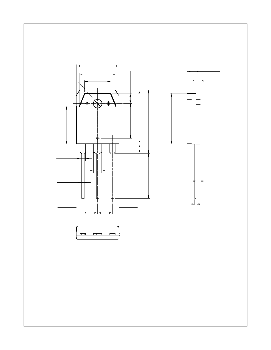
Mechanical Dimensions
TO-3P
15.60
±0.20
4.80
±0.20
13.60
±0.20
9.60
±0.20
2.00
±0.20
3.00
±0.20
1.00
±0.20
1.40
±0.20
ø3.20
±0.10
3.80
±
0.20
13.90
±
0.20
3.50
±
0.20
16.50
±
0.30
12.76
±
0.20
19.90
±
0.20
23.40
±
0.20
18.70
±
0.20
1.50
+0.15
0.05
0.60
+0.15
0.05
5.45TYP
[5.45
±0.30
]
5.45TYP
[5.45
±0.30
]
Dimensions in Millimeters

TRADEMARKS
The following are registered and unregistered trademarks Fairchild Semiconductor owns or is authorized to use and is not intended to
be an exhaustive list of all such trademarks.
9
www.fairchildsemi.com
FGA15N120ANTD Rev. A
F
G
A15N120ANTD 1200V NPT T
r
ench IGBT
DISCLAIMER
FAIRCHILD SEMICONDUCTOR RESERVES THE RIGHT TO MAKE CHANGES WITHOUT FURTHER NOTICE TO ANY
PRODUCTS HEREIN TO IMPROVE RELIABILITY, FUNCTION OR DESIGN. FAIRCHILD DOES NOT ASSUME ANY LIABILITY
ARISING OUT OF THE APPLICATION OR USE OF ANY PRODUCT OR CIRCUIT DESCRIBED HEREIN; NEITHER DOES IT
CONVEY ANY LICENSE UNDER ITS PATENT RIGHTS, NOR THE RIGHTS OF OTHERS. THESE SPECIFICATIONS DO NOT
EXPAND THE TERMS OF FAIRCHILD'S WORLDWIDE TERMS AND CONDITIONS, SPECIFICALLY THE WARRANTY THEREIN,
WHICH COVERS THESE PRODUCTS.
LIFE SUPPORT POLICY
FAIRCHILD'S PRODUCTS ARE NOT AUTHORIZED FOR USE AS CRITICAL COMPONENTS IN LIFE SUPPORT DEVICES OR
SYSTEMS WITHOUT THE EXPRESS WRITTEN APPROVAL OF FAIRCHILD SEMICONDUCTOR CORPORATION.
As used herein:
1. Life support devices or systems are devices or systems which,
(a) are intended for surgical implant into the body, or (b) support
or sustain life, or (c) whose failure to perform when properly used
in accordance with instructions for use provided in the labeling,
can be reasonably expected to result in significant injury to the
user.
2. A critical component is any component of a life support device
or system whose failure to perform can be reasonably expected
to cause the failure of the life support device or system, or to
affect its safety or effectiveness.
PRODUCT STATUS DEFINITIONS
Definition of Terms
Datasheet Identification
Product Status
Definition
Advance Information
Formative or In
Design
This datasheet contains the design specifications for
product development. Specifications may change in
any manner without notice.
Preliminary
First Production
This datasheet contains preliminary data, and
supplementary data will be published at a later date.
Fairchild Semiconductor reserves the right to make
changes at any time without notice in order to improve
design.
No Identification Needed
Full Production
This datasheet contains final specifications. Fairchild
Semiconductor reserves the right to make changes at
any time without notice in order to improve design.
Obsolete
Not In Production
This datasheet contains specifications on a product
that has been discontinued by Fairchild semiconductor.
The datasheet is printed for reference information only.
Rev. I19
FAST
®
FASTrTM
FPSTM
FRFETTM
GlobalOptoisolatorTM
GTOTM
HiSeCTM
I
2
CTM
i-LoTM
ImpliedDisconnectTM
IntelliMAXTM
ISOPLANARTM
LittleFETTM
MICROCOUPLERTM
MicroFETTM
MicroPakTM
MICROWIRETM
MSXTM
MSXProTM
OCXTM
OCXProTM
OPTOLOGIC
®
OPTOPLANARTM
PACMANTM
POPTM
Power247TM
PowerEdgeTM
PowerSaverTM
PowerTrench
®
QFET
®
QSTM
QT OptoelectronicsTM
Quiet SeriesTM
RapidConfigureTM
RapidConnectTM
SerDesTM
ScalarPumpTM
SILENT SWITCHER
®
SMART STARTTM
SPMTM
StealthTM
SuperFETTM
SuperSOTTM-3
SuperSOTTM-6
SuperSOTTM-8
SyncFETTM
TCMTM
TinyLogic
®
TINYOPTOTM
TruTranslationTM
UHCTM
UniFETTM
UltraFET
®
VCXTM
WireTM
ACExTM
ActiveArrayTM
BottomlessTM
Build it NowTM
CoolFETTM
CROSSVOLTTM
DOMETM
EcoSPARKTM
E
2
CMOSTM
EnSignaTM
FACTTM
FACT Quiet SeriesTM
Across the board. Around the world.TM
The Power Franchise
®
Programmable Active DroopTM
Document Outline