
©2005 Fairchild Semiconductor Corporation
1
www.fairchildsemi.com
FGD3N60LSD Rev. A
FGD3
N6
0LS
D
I
G
BT
July 2005
FGD3N60LSD
IGBT
Features
∑ High Current Capability
∑ Very Low Saturation Voltage : V
CE(sat)
= 1.2 V @ I
C
= 3A
∑ High Input Impedance
Applications
∑ HID Lamp Applications
∑ Piezo Fuel Injection Applications
Description
Fairchild's Insulated Gate Bipolar Transistors (IGBTs) provide
very low conduction losses. The device is designed for applica-
tions where very low On-Voltage Drop is a required feature.
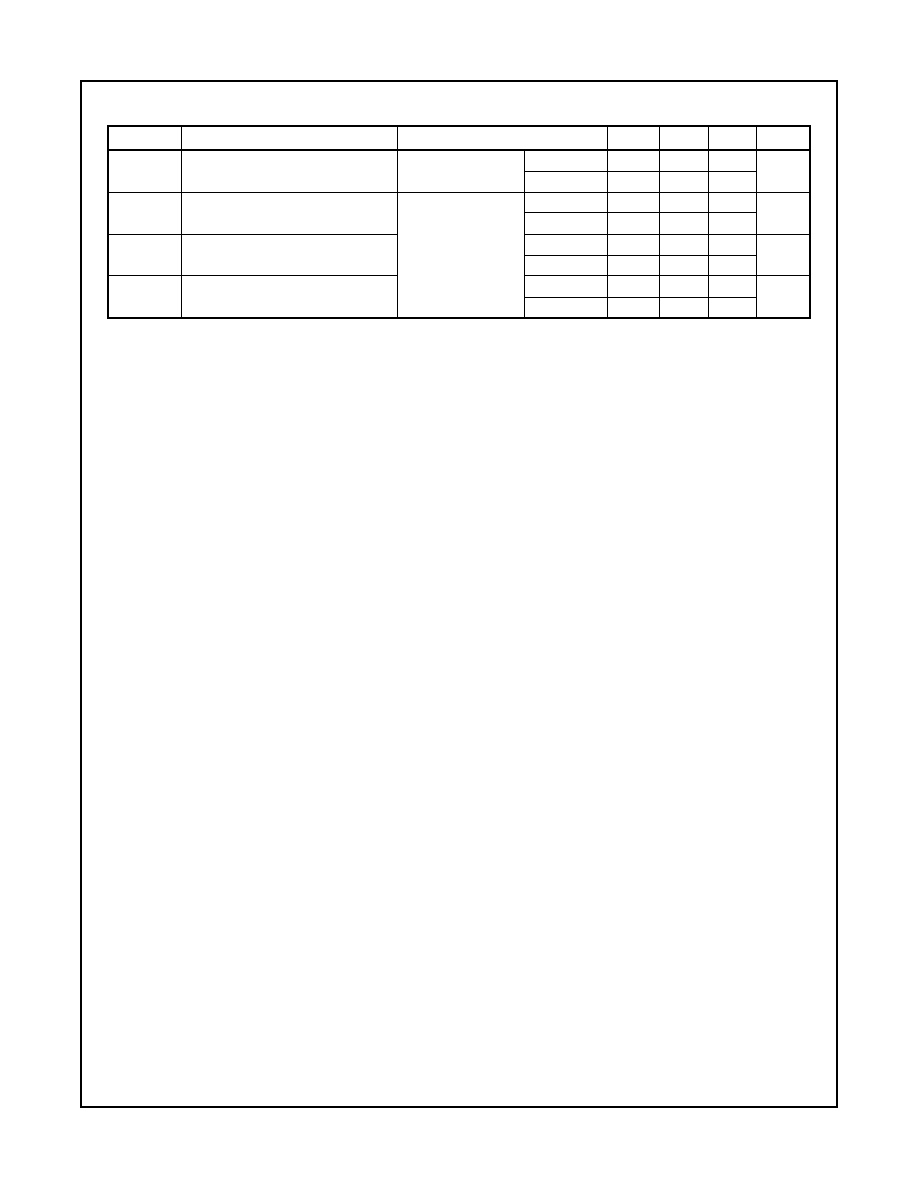
Absolute Maximum Ratings
Notes :
(1) Repetitive rating : Pulse width limited by max. junction temperature
Thermal Characteristics
Notes :
(2) Mounted on 1" squre PCB (FR4 or G-10 Material)
D-PAK
G E
C
G
C
E
G
C
E
Symbol
Description
FGD3N60LSD
Units
V
CES
Collector-Emitter Voltage
600
V
V
GES
Gate-Emitter Voltage
± 20
V
I
C
Collector Current
@ T
C
= 25
∞C
6
A
Collector Current
@ T
C
= 100
∞C
3
A
I
CM (1)
Pulsed Collector Current
25
A
I
F
Diode Continous Forward Current @ T
C
= 100
∞C
3
A
I
FM
Diode Maximum Forward Current
25
A
P
D
Maximum Power Dissipation
@ T
C
= 25
∞C
40
W
Derating Factor
0.32
W/
∞C
T
J
Operating Junction Temperature
-55 to +150
∞C
T
stg
Storage Temperature Range
-55 to +150
∞C
T
L
Maximum Lead Temp. for Soldering
Purposes, 1/8" from Case for 5 Seconds
250
∞C
Symbol
Parameter
Typ.
Max.
Units
R
JC
(IGBT)
Thermal Resistance, Junction-to-Case
--
3.1
∞C/W
R
JA
Thermal Resistance, Junction-to-Ambient (PCB Mount)
(2)
--
100
∞C/W

2
www.fairchildsemi.com
FGD3N60LSD Rev. A
FGD3
N6
0LS
D
I
G
BT
Package Marking and Ordering Information
Electrical Characteristics of the IGBT
T
C
= 25∞C unless otherwise noted
Device Marking
Device
Package
Reel Size
Tape Width
Quantity
FGD3N60LSD
FGD3N60LSDTM
D-PAK
380mm
16mm
2500
FGD3N60LSD
FGD3N60LSDTF
D-PAK
380mm
16mm
2000
Symbol
Parameter
Test Conditions
Min.
Typ.
Max.
Units
Off Characteristics
BV
CES
Collector-Emitter Breakdown Voltage
V
GE
= 0V, I
C
= 250uA
600
--
--
V
B
VCES
/
T
J
Temperature Coefficient of Breakdown]
Voltage
V
GE
= 0V, I
C
= 1mA
--
0.6
--
V/
∞C
I
CES
Collector Cut-Off Current
V
CE
= V
CES
, V
GE
= 0V
--
--
250
uA
I
GES
G-E Leakage Current
V
GE
= V
GES
, V
CE
= 0V
--
--
± 100
nA
On Characteristics
V
GE(th)
G-E Threshold Voltage
I
C
= 3mA, V
CE
= V
GE
2.5
3.2
5.0
V
V
CE(sat)
Collector to Emitter
Saturation Voltage
I
C
= 3A
,
V
GE
= 10V
--
1.2
1.5
V
I
C
= 6A
,
V
GE
= 10V
--
1.8
--
V
Dynamic Characteristics
C
ies
Input Capacitance
V
CE
= 25V
,
V
GE
= 0V,
f = 1MHz
--
185
--
pF
C
oes
Output Capacitance
--
20
--
pF
C
res
Reverse Transfer Capacitance
--
5.5
--
pF
Switching Characteristics
t
d(on)
Turn-On Delay Time
V
CC
= 480 V, I
C
= 3A,
R
G
= 470
, V
GE
= 10V,
Inductive Load, T
C
= 25
∞C
--
40
--
ns
t
r
Rise Time
--
40
--
ns
t
d(off)
Turn-Off Delay Time
--
600
--
ns
t
f
Fall Time
--
600
--
ns
E
on
Turn-On Switching Loss
--
250
--
uJ
E
off
Turn-Off Switching Loss
--
1.00
--
mJ
E
ts
Total
Switching
Loss
--
1.25
--
mJ
t
d(on)
Turn-On Delay Time
V
CC
= 480 V, I
C
= 3A,
R
G
= 470
, V
GE
= 10V,
Inductive Load, T
C
= 125
∞C
--
40
--
ns
t
r
Rise Time
--
45
--
ns
t
d(off)
Turn-Off Delay Time
--
620
--
ns
t
f
Fall Time
--
800
--
ns
E
on
Turn-On Switching Loss
--
300
--
uJ
E
off
Turn-Off Switching Loss
--
1.9
--
mJ
E
ts
Total
Switching
Loss
--
2.2
--
mJ
Q
g
Total Gate Charge
V
CE
= 480 V, I
C
= 3A,
V
GE
= 10V
--
12.5
--
nC
Q
ge
Gate-Emitter Charge
--
2.8
--
nC
Q
gc
Gate-Collector Charge
--
4.9
--
nC
L
e
Internal Emitter Inductance
Measured 5mm from PKG
--
7.5
--
nH
3
www.fairchildsemi.com
FGD3N60LSD Rev. A
FGD3
N6
0LS
D
I
G
BT
Electrical Characteristics of DIODE
T
C
= 25
∞C unless otherwise noted
Symbol
Parameter
Test Conditions
Min.
Typ.
Max. Units
V
FM
Diode Forward Voltage
I
F
= 3A
T
C
= 25
∞C
--
1.5
1.9
V
T
C
= 100
∞C
--
1.55
--
t
rr
Diode Reverse Recovery Time
I
F
= 3A,
di/dt = 100A/us
V
R
= 200V
T
C
= 25
∞C
--
234
--
ns
T
C
= 100
∞C
--
--
--
I
rr
Diode Peak Reverse Recovery Current
T
C
= 25
∞C
--
2.64
--
A
T
C
= 100
∞C
--
--
--
Q
rr
Diode Reverse Recovery Charge
T
C
= 25
∞C
--
309
--
nC
T
C
= 100
∞C
--
--
--

4
www.fairchildsemi.com
FGD3N60LSD Rev. A
FGD3
N6
0LS
D
I
G
BT
Typical Performance Characteristics
Figure 1. Typical Output Characteristics
Figure 2. Typical Output Characteristics
Figure 3. Typical Output Characteristics
Figure 4. Transfer Characteristics
Figure 5. Saturation Voltage vs. Case
Figure 6. Capacitance Characteristics
0
2
4
6
8
0
6
12
18
24
30
20V
15V
10V
V
GE
= 8V
Common Emitter
T
C
= 25
∞
C
C
o
ll
ec
tor
Cu
rr
en
t, I
C
[A
]
Collector-Emitter Voltage, V
CE
[V]
0
2
4
6
8
0
6
12
18
24
30
Common Emitter
T
C
= 125∞C
V
GE
= 8V
20V
15V
10V
Collector-Emitter Voltage, V
CE
[V]
C
o
l
l
e
ct
or C
u
rr
en
t,
I
C
[A
]
1
10
0
2
4
6
8
10
Co
ll
e
c
t
o
r
Cu
r
r
e
n
t,
I
C
[A
]
Common Emitter
V
CE
= 20V
T
C
= 25∞C
T
C
= 125∞C
Gate-Emitter Voltage, V
GE
[V]
0.1
1
10
0
2
4
6
8
10
Collector-Emitter Voltage, V
CE
[V]
Co
ll
e
c
to
r C
u
r
r
en
t,
I
C
[A
]
Common Emitter
V
GE
= 10V
T
C
= 25∞C
T
C
= 125∞C
0
30
60
90
120
150
0
1
2
3
I
C
= 6A
I
C
= 3A
I
C
= 1.5A
Common Emitter
V
GE
= 10V
C
o
ll
ec
t
o
r
-
Em
i
t
t
e
r
Vol
t
ag
e,
V
CE
[V]
Case Temperature, T
C
[
∞
C]
1
10
0
100
200
300
400
500
600
Cres
Coes
Cies
Collector - Emitter Voltage, V
CE
[V]
C
a
p
a
c
i
t
a
nc
e [
p
F]
Com mon Em itter
V
GE
= 0V, f = 1MHz
T
C
= 25
∞
C

5
www.fairchildsemi.com
FGD3N60LSD Rev. A
FGD3
N6
0LS
D
I
G
BT
Typical Performance Characteristics
(Continued)
Figure 7. Gate Charge
Figure 8. Turn-On Characteristics vs. Gate
Resistance
Figure 9. Turn-Off Characteristics vs.
Figure 10. Switching Loss vs. Gate Resistance
Gate Resistance
Figure 11. Turn-On Characteristics vs.
Figure 12. Turn-Off Characteristics vs.
Collector Current
Collector Current
2 00
40 0
6 00
8 00 10 0 0
10
1 00
1 0 00
C om m on E m itte r
V
C C
= 48 0V , V
GE
= 1 0V
I
C
= 3 A
T
C
= 25
∞
C
T
C
= 12 5
∞
C
T o n
T r
S
w
itc
h
in
g T
i
m
e
[n
s]
G ate R esistance, R
G
[
]
0
2
4
6
8
10
12
0
2
4
6
8
10
12
Com m on Em itter
R
L
= 160
Vcc = 480V
T
C
= 25
∞
C
G
a
te -
E
m
i
tter V
o
lta
ge, V
GE
[V
]
Gate Charge, Q
g
[nC]
200
400
600
800 1000
100
1000
10000
Toff
Tf
S
w
i
t
ch
i
n
g
T
i
m
e
[n
s]
Gate Resistance, R
G
[
]
Comm on Em itter
V
CC
= 480V, V
GE
= 10V
I
C
= 3A
T
C
= 25∞C
T
C
= 125∞C
200
400
600
800 1000
10
100
1000
10000
S
w
itchin
g
Lo
ss [
µ
J]
Gate Resistance, R
G
[]
Eon
Eoff
Com m on Em itter
V
CC
= 480V, V
GE
= 10V
I
C
= 3A
T
C
= 25
∞
C
T
C
= 125
∞
C
2
3
4
10
100
Tr
Ton
Sw
it
c
h
i
n
g
T
i
m
e
[
n
s]
Collector Current, I
C
[A]
Common Emitter
Vcc = 480V, V
GE
= 10V
R
G
= 470
T
C
= 25
∞
C
T
C
= 125
∞
C
2
3
4
100
1000
Tf
Toff
Sw
i
t
c
h
i
ng T
i
me
[n
s
]
Collector Current, I
C
[A]
Common Emitter
Vcc = 480 V, V
GE
= 10V
R
G
= 470
T
C
= 25
∞
C
T
C
= 125
∞
C

6
www.fairchildsemi.com
FGD3N60LSD Rev. A
FGD3
N6
0LS
D
I
G
BT
Typical Performance Characteristics
(Continued)
Figure 13. Switching Loss vs. Collector Current
Figure 14. Forward Characteristics
Figure 15. Forward Voltage Drop Vs Tj
Figure 16. SOA Characteristics
Figure 17. Transient Thermal Impedance of IGBT
0
1
2
3
4
0.1
1
10
100
F
o
r
w
ar
d Cur
r
en
t, I
F
[A
]
Forward Voltage Drop, V
F
[V]
Tc = 25
∞
C
Tc = 100
∞
C
2
3
4
100
1000
Eon
Eoff
S
w
it
c
h
in
g Los
s
[
µ
J]
Collector Current, I
C
[A]
Common Emitter
Vcc = 480 V, V
GE
= 10V
R
G
= 470
T
C
= 25
∞
C
T
C
= 125
∞
C
25
50
75
100
125
1.2
1.6
2.0
2.4
2.8
I
F
=3 A
I
F
=6 A
F
o
rward V
o
l
t
age
Drop,
V
F
[V
]
Junction Temperature, Tj [
∞
C]
I
F
=1.5 A
0.1
1
10
100
1000
0.01
0.1
1
10
100
50
µ
s
100
µ
s
1ms
DC Operation
Ic MAX (Pulsed)
Ic MAX (Continuous)
Single Nonrepetitive
Pulse Tc = 25
∞
C
Curves must be derated
linearly with increase
in temperature
C
o
l
l
ec
tor
Cur
r
ent, I
c
[A
]
Collector - Emitter Voltage, V
CE
[V]
1 E -5
1 E -4
1 E -3
0 .0 1
0 .1
1
1 0
0 .0 1
0 .1
1
1 0
R e cta ngula r P uls e D ura tio n [s e c]
Ther
m
a
l
R
e
sponse
[
Z
t
h
j
c
]
0 .5
0 .2
0 .1
0 .0 5
0 .0 2
0 .0 1
s in g le p u ls e
Pdm
t1
t2
Duty factor D = t1 / t2
Peak Tj = Pdm
◊ Zthjc + T
C
7
www.fairchildsemi.com
FGD3N60LSD Rev. A
FGD3
N6
0LS
D
I
G
BT
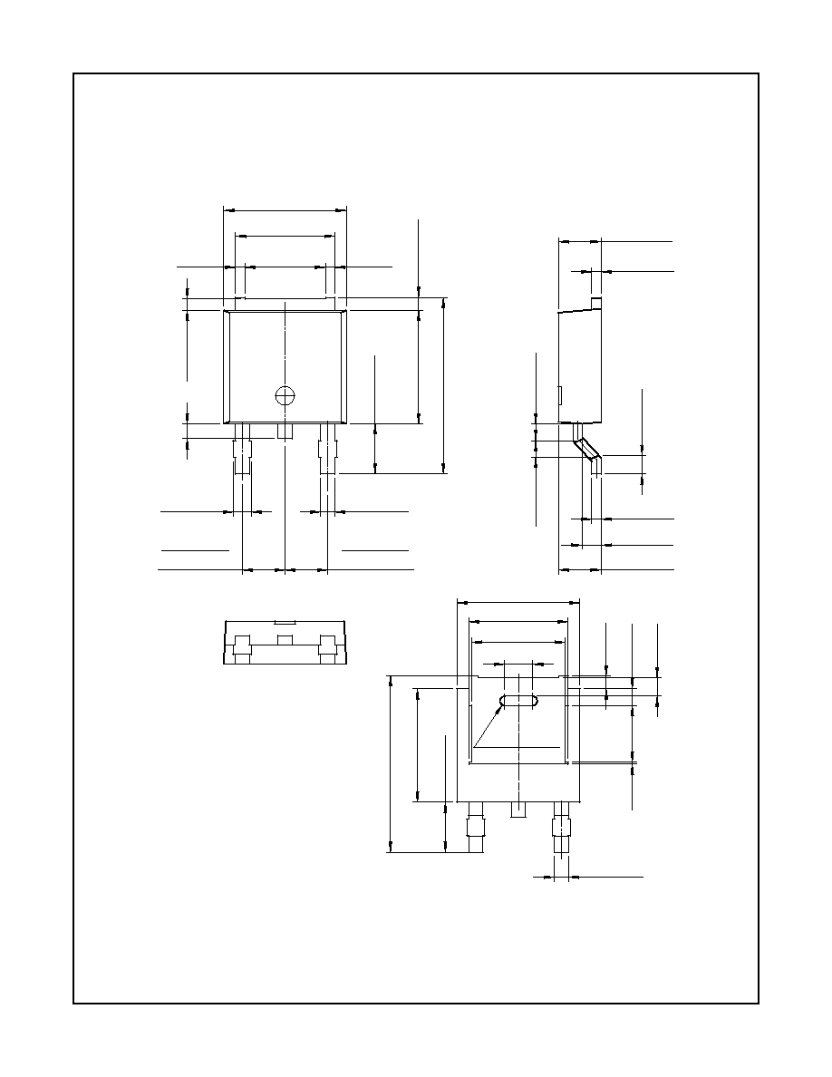
Mechanical Dimensions
6.60
±
0.20
2.30
±
0.10
0.50
±
0.10
5.34
±
0.30
0.70
±
0.20
0.60
±
0.20
0.80
±
0.20
9.50
±
0.30
6.10
±
0.20
2.70
±
0.20
9.50
±
0.30
6.10
±
0.20
2.70
±
0.20
MIN0.55
0.76
±
0.10
0.50
±
0.10
1.02
±
0.20
2.30
±
0.20
6.60
±
0.20
0.76
±
0.10
(5.34)
(1.50)
(2XR0.25)
(5.04)
0.89
±
0.10
(0.10)
(3.05)
(1.00)
(0.90)
(0.70)
0.91
±
0.10
2.30TYP
[2.30
±
0.20]
2.30TYP
[2.30
±
0.20]
MAX0.96
(4.34)
(0.50)
(0.50)
D-PAK
Dimensions in Millimeters
TRADEMARKS
The following are registered and unregistered trademarks Fairchild Semiconductor owns or is authorized to use and is not intended to
be an exhaustive list of all such trademarks.
FGD3
N6
0LS
D
I
G
BT
DISCLAIMER
FAIRCHILD SEMICONDUCTOR RESERVES THE RIGHT TO MAKE CHANGES WITHOUT FURTHER NOTICE TO ANY
PRODUCTS HEREIN TO IMPROVE RELIABILITY, FUNCTION OR DESIGN. FAIRCHILD DOES NOT ASSUME ANY LIABILITY
ARISING OUT OF THE APPLICATION OR USE OF ANY PRODUCT OR CIRCUIT DESCRIBED HEREIN; NEITHER DOES IT
CONVEY ANY LICENSE UNDER ITS PATENT RIGHTS, NOR THE RIGHTS OF OTHERS.
LIFE SUPPORT POLICY
FAIRCHILD'S PRODUCTS ARE NOT AUTHORIZED FOR USE AS CRITICAL COMPONENTS IN LIFE SUPPORT DEVICES OR
SYSTEMS WITHOUT THE EXPRESS WRITTEN APPROVAL OF FAIRCHILD SEMICONDUCTOR CORPORATION.
As used herein:
1. Life support devices or systems are devices or systems which,
(a) are intended for surgical implant into the body, or (b) support
or sustain life, or (c) whose failure to perform when properly used
in accordance with instructions for use provided in the labeling,
can be reasonably expected to result in significant injury to the
user.
2. A critical component is any component of a life support device
or system whose failure to perform can be reasonably expected
to cause the failure of the life support device or system, or to
affect its safety or effectiveness.
PRODUCT STATUS DEFINITIONS
Definition of Terms
Datasheet Identification
Product Status
Definition
Advance Information
Formative or In
Design
This datasheet contains the design specifications for
product development. Specifications may change in
any manner without notice.
Preliminary
First Production
This datasheet contains preliminary data, and
supplementary data will be published at a later date.
Fairchild Semiconductor reserves the right to make
changes at any time without notice in order to improve
design.
No Identification Needed
Full Production
This datasheet contains final specifications. Fairchild
Semiconductor reserves the right to make changes at
any time without notice in order to improve design.
Obsolete
Not In Production
This datasheet contains specifications on a product
that has been discontinued by Fairchild semiconductor.
The datasheet is printed for reference information only.
FAST
Æ
FASTrTM
FPSTM
FRFETTM
GlobalOptoisolatorTM
GTOTM
HiSeCTM
I
2
CTM
i-LoTM
ImpliedDisconnectTM
IntelliMAXTM
ISOPLANARTM
LittleFETTM
MICROCOUPLERTM
MicroFETTM
MicroPakTM
MICROWIRETM
MSXTM
MSXProTM
OCXTM
OCXProTM
OPTOLOGIC
Æ
OPTOPLANARTM
PACMANTM
POPTM
Power247TM
PowerEdgeTM
PowerSaverTM
PowerTrench
Æ
QFET
Æ
QSTM
QT OptoelectronicsTM
Quiet SeriesTM
RapidConfigureTM
RapidConnectTM
µSerDesTM
SILENT SWITCHER
Æ
SMART STARTTM
SPMTM
StealthTM
SuperFETTM
SuperSOTTM-3
SuperSOTTM-6
SuperSOTTM-8
SyncFETTM
TinyLogic
Æ
TINYOPTOTM
TruTranslationTM
UHCTM
UltraFET
Æ
UniFETTM
VCXTM
WireTM
ACExTM
ActiveArrayTM
BottomlessTM
Build it NowTM
CoolFETTM
CROSSVOLTTM
DOMETM
EcoSPARKTM
E
2
CMOSTM
EnSignaTM
FACTTM
FACT Quiet SeriesTM
Across the board. Around the world.TM
The Power Franchise
Æ
Programmable Active DroopTM
Rev. I16
8
www.fairchildsemi.com
FGD3N60LSD Rev. A
FGD3
N6
0LS
D
I
G
BT