 | ÐлекÑÑоннÑй компоненÑ: FGP30N6S2 | СкаÑаÑÑ:  PDF PDF  ZIP ZIP |
Äîêóìåíòàöèÿ è îïèñàíèÿ www.docs.chipfind.ru
©2003 Fairchild Semiconductor Corporation
August 2003
FGH30N6S2 / FGP30N6S2 / FGB30N6S2 Rev. A1
FGH30N6S
2
/
F
G
P30N6S2
/ FGB30N6S2
FGH30N6S2 / FGP30N6S2 / FGB30N6S2
600V, SMPS II Series N-Channel IGBT
General Description
The FGH30N6S2, FGP30N6S2, and FGB30N6S2 are Low
Gate Charge, Low Plateau Voltage SMPS II IGBTs combin-
ing the fast switching speed of the SMPS IGBTs along with
lower gate charge and plateau voltage and avalanche capa-
bility (UIS). These LGC devices shorten delay times, and
reduce the power requirement of the gate drive. These de-
vices are ideally suited for high voltage switched mode pow-
er supply applications where low conduction loss, fast
switching times and UIS capability are essential. SMPS II
LGC devices have been specially designed for:
· Power Factor Correction (PFC) circuits
· Full bridge topologies
· Half bridge topologies
· Push-Pull circuits
· Uninterruptible power supplies
· Zero voltage and zero current switching circuits
Formerly Developmental Type TA49367.
Features
· 100kHz Operation at 390V, 14A
· 200kHZ Operation at 390V, 9A
· 600V Switching SOA Capability
· Typical Fall Time. . . . . . . . . . . 90ns at TJ = 125
o
C
· Low Gate Charge . . . . . . . . . 23nC at V
GE
= 15V
· Low Plateau Voltage . . . . . . . . . . . . . 6.5V Typical
· UIS Rated . . . . . . . . . . . . . . . . . . . . . . . . . 150mJ
· Low Conduction Loss
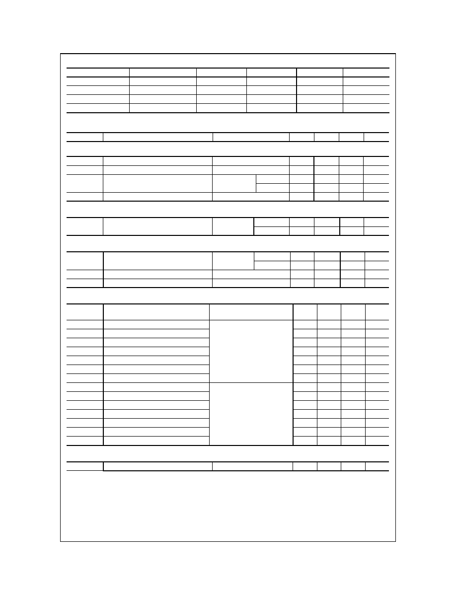
Device Maximum Ratings
T
C
= 25°C unless otherwise noted
Symbol
Parameter
Ratings
Units
BV
CES
Collector to Emitter Breakdown Voltage
600
V
I
C25
Collector Current Continuous, T
C
= 25°C
45
A
I
C110
Collector Current Continuous, T
C
= 110°C
20
A
I
CM
Collector Current Pulsed (Note 1)
108
A
V
GES
Gate to Emitter Voltage Continuous
±20
V
V
GEM
Gate to Emitter Voltage Pulsed
±30
V
SSOA
Switching Safe Operating Area at T
J
= 150°C, Figure 2
60A at 600V
E
AS
Pulsed Avalanche Energy, I
CE
= 20A, L = 1.3mH, V
DD
= 50V
150
mJ
P
D
Power Dissipation Total T
C
= 25°C
167
W
Power Dissipation Derating T
C
> 25°C
1.33
W/°C
T
J
Operating Junction Temperature Range
-55 to 150
°C
T
STG
Storage Junction Temperature Range
-55 to 150
°C
CAUTION: Stresses above those listed in "Device Maximum Ratings" may cause permanent damage to the device. This is a stress only rating and
operation of the device at these or any other conditions above those indicated in the operational sections of this specification is not implied.
NOTE:
1. Pulse width limited by maximum junction temperature.
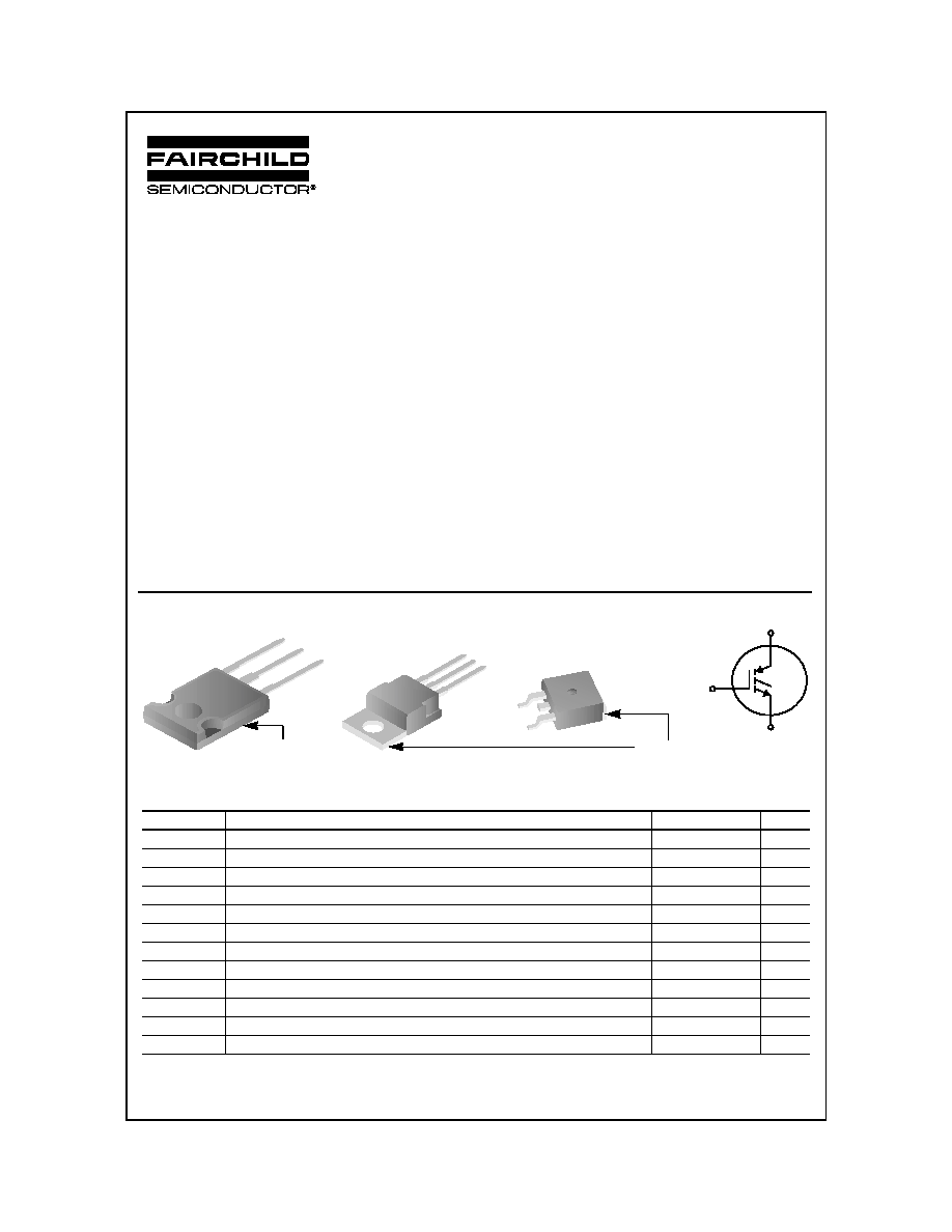
Package
Symbol
C
E
G
TO-247
E
C
G
TO-263AB
TO-220AB
E
C
G
E
G
COLLECTOR
(Flange)
COLLECTOR
(Back-Metal)
©2003 Fairchild Semiconductor Corporation
FGH30N6S2 / FGP30N6S2 / FGS30N6S2 Rev. A1
FGH30N6S
2
/
FGP3
0N6S2 / FGS30N6S
2
Package Marking and Ordering Information
Electrical Characteristics
T
J
= 25°C unless otherwise noted
Off State Characteristics
On State Characteristics
Dynamic Characteristics
Switching Characteristics
Thermal Characteristics
Device Marking
Device
Package
Reel Size
Tape Width
Quantity
30N6S2
FGH30N6S2
TO-247
Tube
N/A
30 Units
30N6S2
FGP30N6S2
TO-220AB
Tube
N/A
50 Units
30N6S2
FGB30N6S2
TO-263AB
Tube
N/A
50 Units
30N6S2
FGB30N6S2T
TO-263AB
330mm
24mm
800 Units
Symbol
Parameter
Test Conditions
Min
Typ
Max
Units
BV
CES
Collector to Emitter Breakdown Voltage
I
C
= 250
µ
A, V
GE
= 0
600
-
-
V
BV
ECS
Emitter to Collector Breakdown Voltage
I
C
= -10mA, V
GE
= 0
20
-
-
V
I
CES
Collector to Emitter Leakage Current
V
CE
= 600V
T
J
= 25°C
-
-
100
µ
A
T
J
= 125°C
-
-
2
mA
I
GES
Gate to Emitter Leakage Current
V
GE
= ± 20V
-
-
±250
nA
V
CE(SAT)
Collector to Emitter Saturation Voltage
I
C
= 12A,
V
GE
= 15V
T
J
= 25°C
-
2.0
2.5
V
T
J
= 125°C
-
1.7
2.0
V
Q
G(ON)
Gate Charge
I
C
= 12A,
V
CE
= 300V
V
GE
= 15V
-
23
29
nC
V
GE
= 20V
-
26
33
nC
V
GE(TH)
Gate to Emitter Threshold Voltage
I
C
= 250
µ
A, V
CE
= 600V
3.5
4.3
5.0
V
V
GEP
Gate to Emitter Plateau Voltage
I
C
= 12A, V
CE
= 300V
-
6.5
8.0
V
SSOA
Switching SOA
T
J
= 150°C, R
G
= 10
,
V
GE
=
15V, L = 100
µ
H, V
CE
= 600V
60
-
-
A
t
d(ON)I
Current Turn-On Delay Time
IGBT and Diode at T
J
= 25°C,
I
CE
= 12A,
V
CE
= 390V,
V
GE
= 15V,
R
G
= 10
L = 200
µ
H
Test Circuit - Figure 20
-
6
-
ns
t
rI
Current Rise Time
-
10
-
ns
t
d(OFF)I
Current Turn-Off Delay Time
-
40
-
ns
t
fI
Current Fall Time
-
53
-
ns
E
ON1
Turn-On Energy (Note 2)
-
55
-
µ
J
E
ON2
Turn-On Energy (Note 2)
-
110
-
µ
J
E
OFF
Turn-Off Energy (Note 3)
-
100
150
µ
J
t
d(ON)I
Current Turn-On Delay Time
IGBT and Diode at T
J
= 125°C
I
CE
= 12A,
V
CE
= 390V,
V
GE
= 15V,
R
G
= 10
L = 200
µ
H
Test Circuit - Figure 20
-
11
-
ns
t
rI
Current Rise Time
-
17
-
ns
t
d(OFF)I
Current Turn-Off Delay Time
-
73
100
ns
t
fI
Current Fall Time
-
90
100
ns
E
ON1
Turn-On Energy (Note 2)
-
55
-
µ
J
E
ON2
Turn-On Energy (Note 2)
-
160
200
µ
J
E
OFF
Turn-Off Energy (Note 3)
-
250
350
µ
J
R
JC
Thermal Resistance Junction-Case
-
-
0.75
°C/W
NOTE:
2.
Values for two Turn-On loss conditions are shown for the convenience of the circuit designer. E
ON1
is the turn-on loss
of the IGBT only. E
ON2
is the turn-on loss when a typical diode is used in the test circuit and the diode is at the same T
J
as the IGBT. The diode type is specified in figure 20.
3.
Turn-Off Energy Loss (E
OFF
) is defined as the integral of the instantaneous power loss starting at the trailing edge of
the input pulse and ending at the point where the collector current equals zero (I
CE
= 0A). All devices were tested per
JEDEC Standard No. 24-1 Method for Measurement of Power Device Turn-Off Switching Loss. This test method produc-
es the true total Turn-Off Energy Loss.
©2003 Fairchild Semiconductor Corporation
FGH30N6S2 / FGP30N6S2 / FGS30N6S2 Rev. A1
FGH30N6S
2
/
FGP3
0N6S2 / FGS30N6S
2
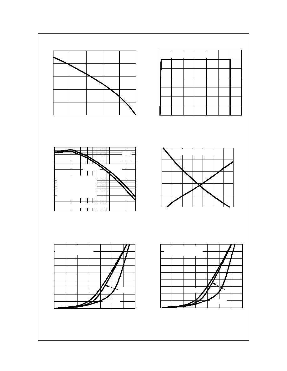
Typical Performance Curves
Figure 1. DC Collector Current vs Case
Temperature
Figure 2. Minimum Switching Safe Operating Area
Figure 3. Operating Frequency vs Collector to
Emitter Current
Figure 4. Short Circuit Withstand Time
Figure 5. Collector to Emitter On-State Voltage
Figure 6. Collector to Emitter On-State Voltage
T
C
, CASE TEMPERATURE (
o
C)
I
CE
,
DC CO
L
L
ECT
O
R CUR
RENT
(A)
50
10
0
20
25
75
100
125
150
40
30
50
V
CE
, COLLECTOR TO EMITTER VOLTAGE (V)
700
0
I
CE
,
CO
L
L
ECT
O
R T
O
EM
I
T
T
E
R CURRENT
(
A
)
300
400
200
100
500
600
0
40
60
20
70
50
30
10
T
J
= 150
o
C, R
G
= 10
, V
GE
= 15V, L = 100
µ
H
f
MAX
, O
PERA
T
ING
F
R
EQ
U
E
NCY (
k
Hz)
1
I
CE
, COLLECTOR TO EMITTER CURRENT (A)
10
30
10
20
1000
100
T
C
75
o
C
T
J
= 125
o
C, R
G
= 3
, L = 200
µ
H, V
CE
= 390V
f
MAX1
= 0.05 / (t
d(OFF)I
+ t
d(ON)I
)
R
ØJC
= 0.49
o
C/W, SEE NOTES
P
C
= CONDUCTION DISSIPATION
(DUTY FACTOR = 50%)
f
MAX2
= (P
D
- P
C
) / (E
ON2
+ E
OFF
)
V
GE
= 10V
V
GE
= 15V
V
GE
, GATE TO EMITTER VOLTAGE (V)
I
SC
,
P
E
AK
SHO
R
T
C
I
RCU
I
T
CU
RRE
NT
(
A
)
t
SC
,
S
H
O
R
T
CI
R
C
U
I
T
W
I
T
H
S
T
AN
D T
I
M
E
(
µ
s)
100
150
200
250
300
350
9
10
11
12
13
14
15
16
2
4
6
8
10
12
V
CE
= 390V, R
G
= 10
, T
J
= 125
o
C
I
SC
t
SC
0.50
1.00
V
CE
, COLLECTOR TO EMITTER VOLTAGE (V)
I
CE
,
CO
L
L
E
C
T
O
R T
O
E
M
I
T
T
E
R CURRE
NT
(A)
0
2
6
1.50
2.25
14
8
18
16
1.25
4
10
12
1.75
PULSE DURATION = 250
µ
s
DUTY CYCLE < 0.5%, V
GE
= 10V
T
J
= 125
o
C
T
J
= 150
o
C
0.75
2.00
T
J
= 25
o
C
I
CE
,
C
O
L
L
EC
T
O
R T
O
EM
I
T
T
E
R
CURRE
NT
(
A
)
V
CE
, COLLECTOR TO EMITTER VOLTAGE (V)
0
18
.5
1
1.50
2.0
2.25
.75
1.75
1.25
2
6
14
8
16
4
10
12
T
J
= 125
o
C
T
J
= 25
o
C
DUTY CYCLE < 0.5%, V
GE
=15V
PULSE DURATION = 250
µ
s
T
J
= 150
o
C
©2003 Fairchild Semiconductor Corporation
FGH30N6S2 / FGP30N6S2 / FGS30N6S2 Rev. A1
FGH30N6S
2
/
FGP3
0N6S2 / FGS30N6S
2
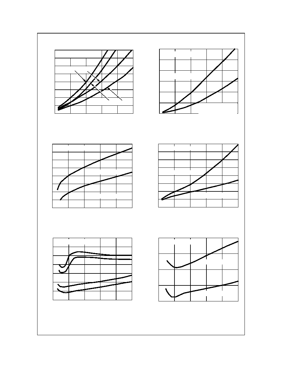
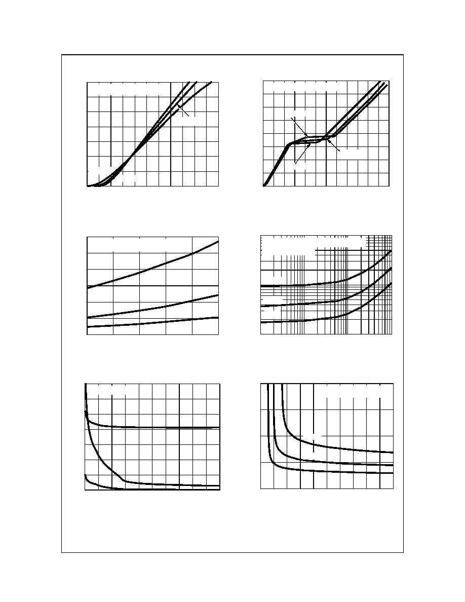
Figure 7. Turn-On Energy Loss vs Collector to
Emitter Current
Figure 8. Turn-Off Energy Loss vs Collector to
Emitter Current
Figure 9. Turn-On Delay Time vs Collector to
Emitter Current
Figure 10. Turn-On Rise Time vs Collector to
Emitter Current
Figure 11. Turn-Off Delay Time vs Collector to
Emitter Current
Figure 12. Fall Time vs Collector to Emitter
Current
Typical Performance Curves
(Continued)
E
ON
2
,
T
URN-O
N
ENERG
Y
L
O
SS (
µ
J)
200
I
CE
, COLLECTOR TO EMITTER CURRENT (A)
100
250
0
5
10
15
20
25
0
350
300
50
400
T
J
= 125
o
C, V
GE
= 10V, V
GE
= 15V
T
J
= 25
o
C, V
GE
= 10V, V
GE
= 15V
150
R
G
= 10
, L = 500
µ
H, V
CE
= 390V
E
OF
F
T
URN-
O
F
F
ENERG
Y
L
O
SS
(
µ
J)
I
CE
, COLLECTOR TO EMITTER CURRENT (A)
100
300
0
600
5
10
15
20
25
0
500
400
200
R
G
= 10
, L = 500
µ
H, V
CE
= 390V
T
J
= 125
o
C, V
GE
= 10V, V
GE
= 15V
T
J
= 25
o
C, V
GE
= 10V, V
GE
= 15V
I
CE
, COLLECTOR TO EMITTER CURRENT (A)
t
d(
ON
)I
,
T
URN
-O
N
DEL
A
Y T
I
M
E
(n
s
)
0
6
8
12
14
5
10
15
20
25
0
16
4
2
10
R
G
= 10
, L = 500
µ
H, V
CE
= 390V
T
J
= 25
o
C, T
J
= 125
o
C, V
GE
= 10V
T
J
= 25
o
C, T
J
= 125
o
C, V
GE
= 15V
I
CE
, COLLECTOR TO EMITTER CURRENT (A)
t
rI
,
R
ISE TIME
(ns
)
0
20
10
40
35
25
5
10
15
20
25
0
30
15
T
J
= 25
o
C, V
GE
= 10V, V
GE
=15V
T
J
= 125
o
C, V
GE
= 15V, V
GE
= 10V
R
G
= 10
, L = 500
µ
H, V
CE
= 390V
5
20
30
40
50
60
70
80
90
0
5
10
15
20
25
t
d(O
F
F
)
T
URN
-O
F
F
DEL
A
Y
T
I
M
E
(
n
s
)
I
CE
, COLLECTOR TO EMITTER CURRENT (A)
R
G
= 10
, L = 500
µ
H, V
CE
= 390V
I
CE
, COLLECTOR TO EMITTER CURRENT (A)
t
fI
, F
A
LL T
I
M
E
(
n
s
)
40
60
80
100
10
5
15
20
25
0
120
R
G
= 10
, L = 500
µ
H, V
CE
= 390V
T
J
= 125
o
C, V
GE
= 10V OR 15V
T
J
= 25
o
C, V
GE
= 10V OR 15V
©2003 Fairchild Semiconductor Corporation
FGH30N6S2 / FGP30N6S2 / FGS30N6S2 Rev. A1
FGH30N6S
2
/
FGP3
0N6S2 / FGS30N6S
2
Figure 13. Transfer Characteristic
Figure 14. Gate Charge
Figure 15. Total Switching Loss vs Case
Temperature
Figure 16. Total Switching Loss vs Gate
Resistance
Figure 17. Capacitance vs Collector to Emitter
Voltage
Figure 18. Collector to Emitter On-State Voltage vs
Gate to Emitter Voltage
Typical Performance Curves
(Continued)
I
CE
,
CO
L
L
ECT
O
R T
O
EM
I
T
T
E
R
CURRENT
(
A
)
0
25
50
7
9
16
75
150
5
125
100
175
6
8
10
11
12
13
14
15
PULSE DURATION = 250
µ
s
DUTY CYCLE < 0.5%, V
CE
= 10V
T
J
= -55
o
C
T
J
= 125
o
C
V
GE
, GATE TO EMITTER VOLTAGE (V)
T
J
= 25
o
C
V
GE
, G
A
T
E
T
O
E
M
IT
T
E
R V
O
L
T
A
GE
(
V
)
Q
G
, GATE CHARGE (nC)
2
10
0
6
4
8
12
2
6
10
12
0
14
16
14
16
18
24
4
8
20
I
G(REF)
= 1mA, R
L
= 25
, T
J
= 25
o
C
V
CE
= 200V
V
CE
= 400V
V
CE
= 600V
22
I
CE
= 6A
0
0.6
50
75
100
T
C
, CASE TEMPERATURE (
o
C)
0.8
125
25
1.2
E
TOT
A
L
,
T
O
T
A
L
SW
I
T
CHI
N
G
ENE
R
G
Y
L
O
SS (
m
J
)
1.0
I
CE
= 24A
I
CE
= 12A
0.4
0.2
R
G
= 10
, L = 500
µ
H, V
CE
= 390V, V
GE
= 15V
E
TOTAL
= E
ON2
+ E
OFF
150
0.1
10
100
R
G
, GATE RESISTANCE (
)
1.0
1000
E
TO
T
A
L
, T
O
T
A
L S
W
IT
C
H
IN
G
EN
ER
G
Y
L
O
SS
(m
J
)
10
1
E
TOTAL
= E
ON2
+ E
OFF
T
J
= 125
o
C, L = 500
µ
H, V
CE
= 390V, V
GE
= 15V
I
CE
= 24A
I
CE
= 12A
I
CE
= 6A
V
CE
, COLLECTOR TO EMITTER VOLTAGE (V)
C,
CAP
A
C
I
T
ANCE
(
n
F
)
C
RES
0
10
20
30
40
50
0.0
0.4
1.2
1.4
0.8
C
OES
C
IES
60
70
80
90
100
0.2
0.6
1.0
FREQUENCY = 1MHz
1.5
2.0
2.5
3.0
3.5
6
7
8
9
10
11
12
13
14
15
16
V
GE
, GATE TO EMITTER VOLTAGE (V)
V
CE
, C
O
L
L
EC
T
O
R
T
O
EMITT
E
R
V
O
L
T
A
G
E (V)
I
CE
= 12A
I
CE
= 6A
I
CE
= 24A
PULSE DURATION = 250
µ
s
DUTY CYCLE < 0.5%, V
CE
= 10V