©2006 Fairchild Semiconductor Corporation
1
www.fairchildsemi.com
FGP7N60RUFD Rev. A
F
G
P7
N60RUFD 6
0
0V
, 7A RUF IGBT CO-P
AK
January 2006
FGP7N60RUFD
600V, 7A RUF IGBT CO-PAK
Features
∑ High speed switching
∑ Low saturation voltage : V
CE(sat)
= 1.95 V @ I
C
= 7A
∑ High input impedance
∑ CO-PAK, IGBT with FRD : t
rr
= 50 ns (typ.)
∑ Short Circuit rated
Applications
Motor controls and general purpose inverters.
Description
Fairchild's Insulated Gate Bipolar Transistors (IGBTs) provides
low conduction and switching losses.The device is designed for
Motor applications where ruggedness is a required feature.
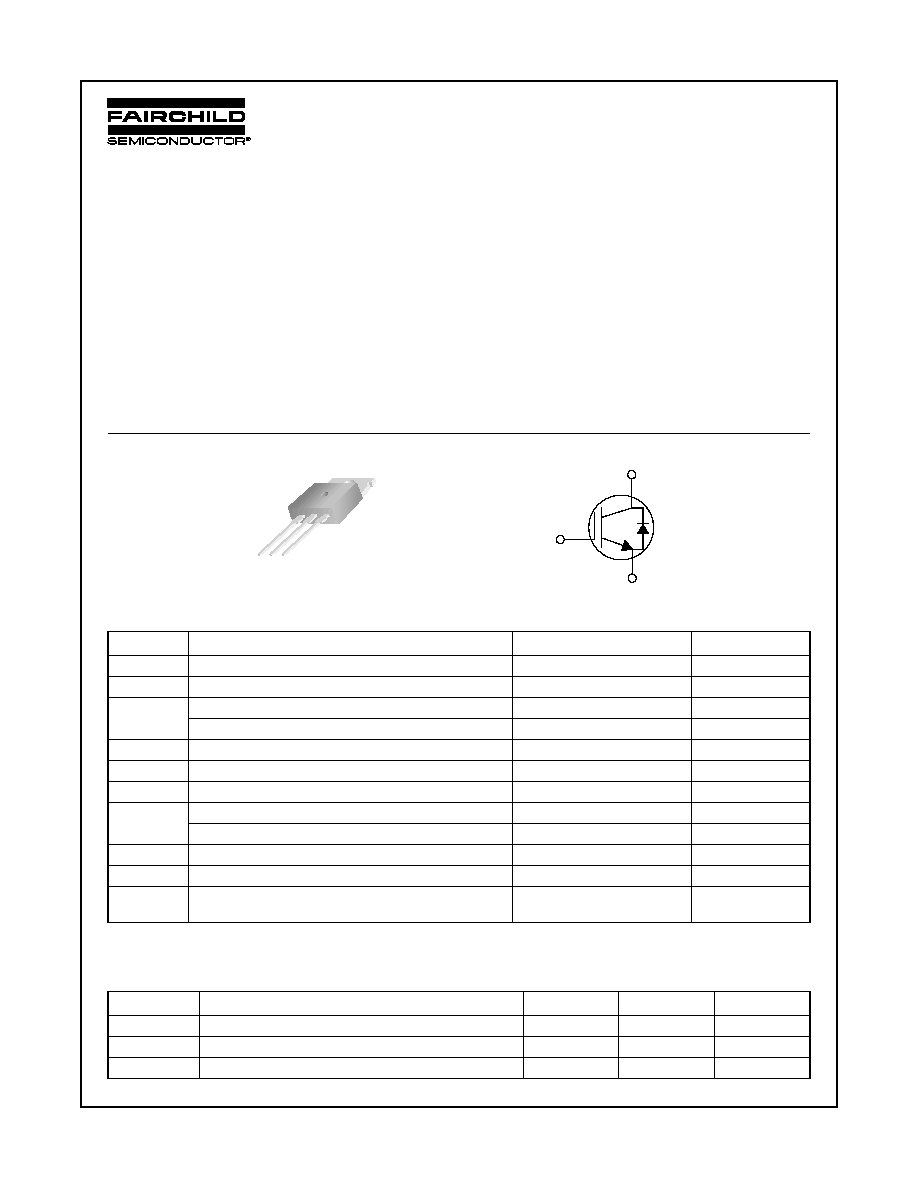
1
TO-220
1.Gate 2.Collector 3.Emitter
C
E
G
Absolute Maximum Ratings
Symbol
Description
FGP7N60RUFD
Units
V
CES
Collector-Emitter Voltage
600
V
V
GES
Gate-Emitter Voltage
± 20
V
I
C
Collector Current
@ T
C
= 25
∞C
14
A
Collector Current
@ T
C
= 100
∞C
7
A
I
CM (1)
Pulsed Collector Current
21
A
I
F
Diode Continuous Forward Current
@ T
C
= 100
∞C
12
A
I
FM
Diode Maximum Forward Current
60
A
P
D
Maximum Power Dissipation
@ T
C
= 25
∞C
69
W
Maximum Power Dissipation
@ T
C
= 100
∞C
28
W
T
J
Operating Junction Temperature
-55 to +150
∞C
T
stg
Storage Temperature Range
-55 to +150
∞C
T
L
Maximum Lead Temp. for soldering
Purposes, 1/8" from case for 5 seconds
300
∞C
Notes :
(1) Repetitive rating : Pulse width limited by max. junction temperature
Thermal Characteristics
Symbol
Parameter
Typ.
Max.
Units
R
JC
(IGBT)
Thermal Resistance, Junction-to-Case
--
1.8
∞C/W
R
JC
(DIODE)
Thermal Resistance, Junction-to-Case
--
3.0
∞C/W
R
JA
Thermal Resistance, Junction-to-Ambient
--
62.5
∞C/W

2
www.fairchildsemi.com
FGP7N60RUFD Rev. A
F
G
P7
N60RUFD 6
0
0V
, 7A RUF IGBT CO-P
AK
Package Marking and Ordering Information
Device Marking
Device
Package
Packaging
Type
Qty per Tube
Max Qty
per Box
FGP7N60RUFD
FGP7N60RUFDTU
TO-220
Rail / Tube
50ea
-
Electrical Characteristics of the IGBT
T
C
= 25∞C unless otherwise noted
Symbol
Parameter
Test Conditions
Min.
Typ.
Max.
Units
Off Characteristics
BV
CES
Collector-Emitter Breakdown Voltage
V
GE
= 0V, I
C
= 250uA
600
--
--
V
B
VCES
/
T
J
Temperature Coefficient of Breakdown
Voltage
V
GE
= 0V, I
C
= 3mA
--
0.6
--
V/
∞C
I
CES
Collector Cut-Off Current
V
CE
= V
CES
, V
GE
= 0V
--
--
250
uA
I
GES
G-E Leakage Current
V
GE
= V
GES
, V
CE
= 0V
--
--
± 100
nA
On Characteristics
V
GE(th)
G-E Threshold Voltage
I
C
= 7mA, V
CE
= V
GE
5.0
6.5
8.0
V
V
CE(sat)
Collector to Emitter
Saturation Voltage
I
C
= 7A
,
V
GE
= 15V
--
1.95
2.8
V
I
C
= 7A
,
V
GE
= 15V,
T
C
= 125
∞C
--
2.1
--
V
I
C
= 14 A
,
V
GE
= 15V
--
2.65
--
V
Dynamic Characteristics
C
ies
Input Capacitance
V
CE
= 30V
,
V
GE
= 0V,
f = 1MHz
--
510
--
pF
C
oes
Output Capacitance
--
55
--
pF
C
res
Reverse Transfer Capacitance
--
15
--
pF
Switching Characteristics
t
d(on)
Turn-On Delay Time
V
CC
= 300 V, I
C
= 7A,
R
G
= 30
, V
GE
= 15V,
Inductive Load, T
C
= 25
∞C
--
60
--
ns
t
r
Rise Time
--
60
--
ns
t
d(off)
Turn-Off Delay Time
--
60
80
ns
t
f
Fall Time
--
170
280
ns
E
on
Turn-On Switching Loss
--
0.23
--
mJ
E
off
Turn-Off Switching Loss
--
0.10
--
mJ
E
ts
Total Switching Loss
--
0.33
0.5
mJ
t
d(on)
Turn-On Delay Time
V
CC
= 300 V, I
C
= 7 A,
R
G
=30
, V
GE
= 15V,
Inductive Load, T
C
= 125
∞C
--
65
--
ns
t
r
Rise Time
--
70
--
ns
t
d(off)
Turn-Off Delay Time
--
55
--
ns
t
f
Fall Time
--
350
--
ns
E
on
Turn-On Switching Loss
--
0.25
--
mJ
E
off
Turn-Off Switching Loss
--
0.27
--
mJ
E
ts
Total Switching Loss
--
0.52
--
mJ
Q
g
Total Gate Charge
V
CE
= 300 V, I
C
= 7A,
V
GE
= 15V
--
24
36
nC
Q
ge
Gate-Emitter Charge
--
4
6
nC
Q
gc
Gate-Collector Charge
--
10
15
nC
L
e
Internal Emitter Inductance
Measured 5mm from PKG
--
7.5
--
nH

3
www.fairchildsemi.com
FGP7N60RUFD Rev. A
F
G
P7
N60RUFD 6
0
0V
, 7A RUF IGBT CO-P
AK
Electrical Characteristics of DIODE
T
C
= 25
∞C unless otherwise noted
Symbol
Parameter
Test Conditions
Min.
Typ.
Max.
Units
V
FM
Diode Forward Voltage
I
F
= 7A
T
C
= 25
∞C
--
1.65
2.1
V
T
C
= 100
∞C
--
1.58
--
t
rr
Diode Reverse Recovery Time
I
F
= 7A
dI/dt = 200 A/
µs
T
C
= 25
∞C
--
50
65
ns
T
C
= 100
∞C
--
58
--
I
rr
Diode Peak Reverse Recovery Current
T
C
= 25
∞C
--
2.5
3.75
A
T
C
= 100
∞C
--
3.3
--
Q
rr
Diode Reverse Recovery Charge
T
C
= 25
∞C
--
62.5
122
nC
T
C
= 100
∞C
--
95.7
--

4
www.fairchildsemi.com
FGP7N60RUFD Rev. A
F
G
P7
N60RUFD 6
0
0V
, 7A RUF IGBT CO-P
AK
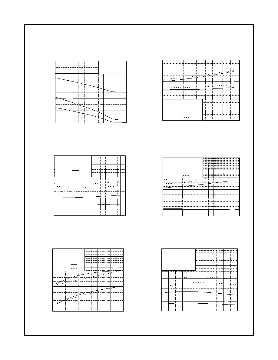
Typical Performance Characteristics
Figure 1. Typical Output Characteristics
Figure 2. Typical Saturation Voltage
Characteristics
0
2
4
6
8
0
10
20
30
40
V
GE
= 8V
T
C
= 25
o
C
Col
l
ec
tor
Cu
rr
ent,
I
C
[A
]
Collector-Emitter Voltage, V
CE
[V]
20V
15V
12V
10V
0
2
4
6
8
0
1 0
2 0
3 0
4 0
C o m m o n E m itte r
V
G e
= 1 5 V
T c = 2 5
o
C
T c = 1 2 5
o
C
C o lle cto r-E m itte r V o lta ge , V
c e
[V ]
C
o
llec
t
or Curr
ent,
I
C
[A
]
Figure 3. Saturation Voltage vs Case
Figure 4. Load Current vs Frequency
Temperature at Variant Current Level
0
25
50
75
100
125
150
1
2
3
4
Ic = 14 A
Ic = 7 A
Ic =3.5 A
Collector - Em
itter Voltage, V
CE
[V]
Case Temperature, Tc [
o
C]
Com m om Em itter
V
GE
= 15V
0.1
1
10
100
1000
0
5
10
15
Vcc = 300V
load Current : peak of square wave
Duty cycle : 50%
Tc = 100
o
C
Power Dissipation = 14W
Lo
ad
C
u
rr
en
t
[
A
]
Frequency [kHz]
Figure 5. Saturation Voltage vs. Vge
Figure 6. Saturation Voltage vs. Vge
5
10
15
20
2
4
6
8
10
Common Emitter
T
C
= 25
o
C
Ic=3.5A
Gate - Emitter Voltage, V
GE
[V]
Collect
or
- Emitt
e
r Voltage,
V
CE
[V]
7A
14A
5
10
15
20
0
2
4
6
8
10
C om m on E m itter
T c = 125
o
C
G ate - Em itter V oltage, V
G E
[V]
Collector - Emitt
e
r V
o
lt
age, V
CE
[V
]
Ic=3.5A
7A
14A
5
www.fairchildsemi.com
FGP7N60RUFD Rev. A
F
G
P7
N60RUFD 6
0
0V
, 7A RUF IGBT CO-P
AK
Typical Performance Characteristics
(Continued)
Figure 7. Capacitance Characteristics
Figure 8. Turn-On Characteristics vs. Gate
Temperature at Variant Current Level
Resistance
1
10
0
200
400
600
800
1000
Crss
Coss
Ciss
Common Emitter
V
GE
= 0V, f = 1MHz
T
C
= 25
o
C
Collector-Emitter Voltage, V
CE
[V]
Ca
pacitance
[pF
]
1 0
1 0 0
1 0
1 0 0
C o m m o n E m itte r
V
CC
= 3 0 0 V , V
GE
= + /-1 5 V
I
C
= 7 A
T c = 2 5
o
C
T c = 1 2 5
o
C
T r
T o n
Switchin
g Time [n
s]
G a te R esistance, R
G
[ ]
Figure 9. Turn-Off Characteristics vs.
Figure 10. Switching Loss vs. Gate Resistance
Gate Resistance
10
100
1000
Tf
Toff
Gate Resistance, R
G
[
]
S
w
it
ch
ing
T
i
me
[
n
s]
Comm on Emitter
V
CC
= 300V, V
GE
= +/-15V
I
C
= 7A
Tc = 25
o
C
Tc = 125
o
C
100
Tf
Toff
1 0
1 0 0
2 0 0
3 0 0
4 0 0
5 0 0
6 0 0
E o n
E o n
E o ff
100
E o ff
G a te R e sista nce , R
G
[
]
S
w
itc
h
in
g Lo
ss [
uJ]
C o m m o n E m itte r
V
C C
= 3 0 0 V , V
G E
= + /-1 5 V
I
C
= 7 A
T c = 2 5
o
C
T c = 1 2 5
o
C
Figure 11. Turn-On Characteristics vs.
Figure 12. Turn-Off Characteristics vs.
Collector Current
Collector Current
4
6
8
10
12
14
50
100
150
200
Tr
Ton
Swi
t
chi
ng Ti
me [ns
]
Collector Current, I
C
[A]
Common Emitter
V
GE
= +/-15V, R
G
=30
I
C
= 7A
Tc = 25
o
C
Tc = 125
o
C
4
6
8
10
12
14
200
400
600
800
1000
Collector Current, I
C
[A]
Sw
it
ch
in
g T
i
me [
n
s]
Toff
Tf
Toff
Tf
Com m on Em itter
V
GE
= +/-15V, R
G
=30
I
C
= 7A
Tc = 25
o
C
Tc = 125
o
C