 | ÐлекÑÑоннÑй компоненÑ: FHP3450 | СкаÑаÑÑ:  PDF PDF  ZIP ZIP |
Äîêóìåíòàöèÿ è îïèñàíèÿ www.docs.chipfind.ru
FHP3350, FHP3450 Rev. 1A
1
www.fairchildsemi.com
FHP3350,
FHP3450 T
riple and Quad
V
olta
g
e
Feedbac
k Amplifier
s
tm
June 2006
FHP3350, FHP3450
Triple and Quad Voltage Feedback Amplifiers
Features at ±5V
0.1dB gain flatness to 30MHz
0.07%/0.03° differential gain/phase error
210MHz full power -3dB bandwidth at G = 2
1,100V/µs slew rate
±55mA output current (drives dual video load)
±83mA output short circuit current
Output swings to within 1.3V of either rail
3.6mA supply current per amplifier
Minimum stable gain of 3dB or 1.5V/V
FHP3350 - improved replacement for RC6333
FHP3450 - improved replacement for RC6334
Fully specified at +5V, and ±5V supplies
Applications
Video driver
RGB driver
ADC buffer
S-video amp
Active Filters
Description
The FHP3350 and FHP3450 are low cost, high performance,
voltage feedback amplifiers designed for video applications.
These triple and quad amplifiers consume only 3.6mA of supply
current per channel and are capable of driving dual (75
) video
loads while providing 0.1dB of gain flatness to 30MHz.
Consumer video applications will also benefit from their low
0.07% differential gain and 0.03° differential phase errors. The
FHP3350 offers three outputs that can be put into a high
impedance disable state to allow for video multiplexing or
minimize power consumption.
These amplifiers are designed to operate from 5V (±2.5V) to
12V (±6V) supplies. The outputs swing to within 1.3V of either
supply rail to accommodate video signals on a single 5V supply.
The FHP3350 and FHP3450 are designed on a complementary
bipolar process. They provide 210MHz of full power bandwidth
and 1,100V/µs of slew rate at a supply voltage of ±5V. The
combination of high performance, low power, and excellent
video performance make these amplifiers well suited for use in
many digital consumer video appliances as well as many
general purpose high speed applications.
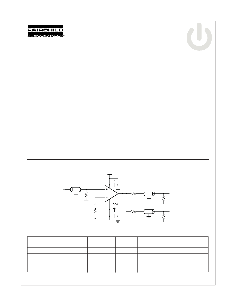
Typical Application Driving Dual Video Loads
Ordering Information
Moisture sensitivity level for all parts is MSL-1.
Part Number
Package
Lead Free
Operating Temp
Range
Packaging
Method
FHP3350IMTC14X
TSSOP-14
Yes
-40°C to +85°C
Reel
FHP3350IM14X
SOIC-14
Yes
-40°C to +85°C
Reel
FHP3450IMTC14X
TSSOP-14
Yes
-40°C to +85°C
Reel
FHP3450IM14X
SOIC-14
Yes
-40°C to +85°C
Reel
+IN
OUT
+Vs
-Vs
Rg
Rf
75
75
Cabl
75
Cable
75
75
OUT
75
Cable
75
75
e
www.fairchildsemi.com
2
FHP3350, FHP3450 Rev. 1A
FHP3350,
FHP3450 T
riple and Quad
V
olta
g
e
Feedbac
k Amplifier
s
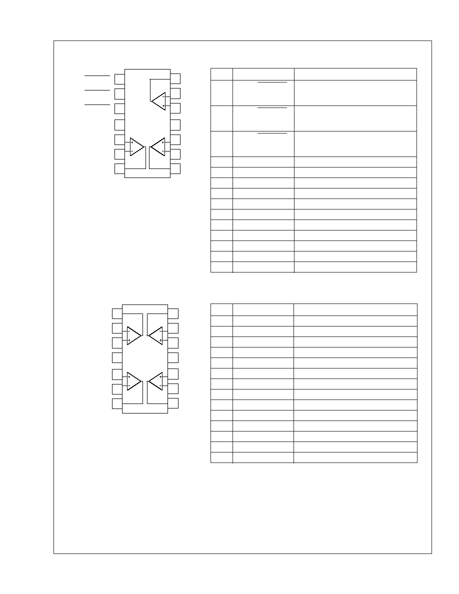
FHP3350 Pin Configurations
FHP3450 Pin Configurations
FHP3350 Pin Assignments
Pin#
Pin
Description
1
NC or DISABLE1
Channel 1 ENABLED if pin is left open or
pulled above V
ON
, DISABLED if pin is
grounded or pulled below V
OFF
2
NC or DISABLE2
Channel 2 ENABLED if pin is left open or
pulled above V
ON
, DISABLED if pin is
grounded or pulled below V
OFF
3
NC or DISABLE3
Channel 3 ENABLED if pin is left open or
pulled above V
ON
, DISABLED if pin is
grounded or pulled below V
OFF
4
+Vs
Positive supply
5
+IN1
Positive Input, channel 1
6
-IN1
Negative Input, channel 1
7
OUT1
Output, channel 1
8
OUT3
Output, channel 3
9
-IN3
Negative Input, channel 3
10
+IN3
Positive Input, channel 3
11
-Vs
Negative supply
12
+IN2
Positive Input, channel 2
13
-IN2
Negative Input, channel 2
14
OUT2
Output, channel 2
FHP3450 Pin Assignments
Pin#
Pin
Description
1
OUT1
Output, channel 1
2
-IN1
Negative Input, channel 1
3
+IN1
Positive Input, channel 1
4
+Vs
Positive supply
5
+IN2
Positive Input, channel 2
6
-IN2
Negative Input, channel 2
7
OUT2
Output, channel 2
8
OUT3
Output, channel 3
9
-IN3
Negative Input, channel 3
10
+IN3
Positive Input, channel 3
11
-Vs
Negative supply
12
+IN4
Positive Input, channel 4
13
-IN4
Negative Input, channel 4
14
OUT4
Output, channel 4
2
3
4
11
12
13
14
OUT4
1
OUT1
FHP3450
TSSOP
6
7
5
8
9
10
+Vs
+IN2
-IN2
OUT2
-IN4
+IN4
-Vs
+IN3
-IN3
OUT3
-IN1
+IN1
2
3
4
11
12
13
14
OUT2
1
NC or DISABLE1
FHP3350
TSSOP-14
6
7
5
8
9
10
+Vs
+IN1
-IN1
OUT1
-IN2
+IN2
-Vs
+IN3
-IN3
OUT3
NC or DISABLE2
NC or DISABLE3
FHP3350, FHP3450 Rev. 1A
3
www.fairchildsemi.com
FHP3350,
FHP3450 T
riple and Quad
V
olta
g
e
Feedbac
k Amplifier
s
Absolute Maximum Ratings
The "Absolute Maximum Ratings" are those values beyond which the safety of the device cannot be guaranteed. The device should
not be operated at these limits. The parametric values defined in the Electrical Characteristics tables are not guaranteed at the
absolute maximum ratings. The "Recommended Operating Conditions" table defines the conditions for actual device operation.
Reliability Information
Note:
1. Package thermal resistance (
JA
), JDEC standard, multi-layer test boards, still air. Assumed power is concentrated in one channel
JA
will be lower,
if power is distributed in all channels.
ESD Protection
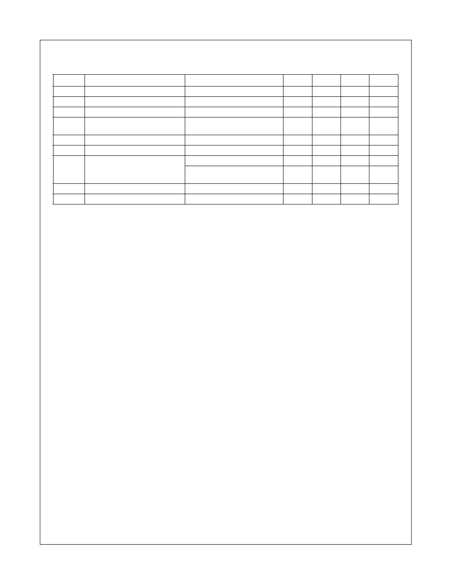
Recommended Operating Conditions
Parameter
Min.
Max.
Unit
Supply Voltage
0
12.6
V
Input Voltage Range
-V
s
- 0.5V
+V
s
+0.5V
V
Parameter
Min.
Typ.
Max.
Unit
Junction Temperature
150
°C
Storage Temperature Range
-65
150
°C
Lead Temperature (Soldering, 10s)
300
°C
14-Lead TSSOP
1
160
°C/W
14-Lead SOIC
1
148
°C/W
ESD Protection
FHP3350
FHP3450
Package
SOIC
TSSOP
SOIC
TSSOP
Human Body Model (HBM)
1500V
1500V
2000V
2000V
Charged Device Model (CDM)
2000V
1500V
2000V
1500V
Parameter
Min.
Typ.
Max.
Unit
Operating Temperature Range
-40
+85
°C
Supply Voltage Range
3
12
V
www.fairchildsemi.com
4
FHP3350, FHP3450 Rev. 1A
FHP3350,
FHP3450 T
riple and Quad
V
olta
g
e
Feedbac
k Amplifier
s
Electrical Characteristics at +5V
T
c
= 25°C, V
s
= 5V, R
f
= 249
,
R
L
= 150
to V
s
/2, G = 2; unless otherwise noted.
Symbol
Parameter
Conditions
Min
Typ
Max
Units
Frequency Domain Response
BW
ss
-3dB Bandwidth
No Peaking, G = +2, V
OUT
= 0.2V
pp
190
MHz
BW
Ls
Full Power Bandwidth
No Peaking, G = +2, V
OUT
= 2V
pp
190
MHz
BW
0.1dB
0.1dB Gain Flatness - Large Signal
G = +2, V
OUT
= 2V
pp
35
MHz
Time Domain Response
t
R
, t
F
Rise and Fall Time
V
OUT
= 0.2V step
2.0
ns
t
S
Settling Time to 0.1%
V
OUT
= 2V step
20
ns
OS
Overshoot
V
OUT
= 0.2V step
2.5
%
SR
Slew Rate
2V step. G = -1
800
V/
µ
s
Distortion / Noise Response
HD2
2nd Harmonic Distortion
V
OUT
= 2V
pp
, 5MHz
-70
dBc
HD3
3rd Harmonic Distortion
V
OUT
= 2V
pp
, 5MHz
-80
dBc
THD
Total Harmonic Distortion
V
OUT
= 2V
pp
, 5MHz
-69
dB
DG
Differential Gain
NTSC (3.58MHz); AC coupled
0.08
%
DP
Differenital Phase
NTSC (3.58MHz); AC coupled
0.02
°
e
n
Input Voltage Noise
> 100kHz
8.5
nV/Hz
i
n
Input Current Noise
> 100kHz
1
pA/Hz
X
TALK
Crosstalk
at 5MHz
-70
dB
DC Performance
V
IO
Input Offset Voltage
1
mV
dV
IO
Average Drift
10
µ
V/°C
I
bn
Input Bias Current
±50
nA
dI
bn
Average Drift
0.33
nA/°C
I
IO
Input Offset Current
±50
nA
PSRR
Power Supply Rejection Ratio
DC
75
dB
A
OL
Open Loop Gain
DC
55
dB
I
S
Supply Current per Amplifier
3.0
mA
I
SD
Disable Supply Current per Amp
Disable Mode
35
µ
A
Disable Characteristics
OFF
ISO
Off Isolation
5MHz
-60
dB
OFFC
OUT
Off Output Capacitance
3
pF
CH
ISO
Channel-to-Channel Isolation
5MHz
-85
dB
T
ON
Turn on time
300
ns
T
OFF
Turn off time
80
ns
V
OFF
Power Down Input Voltage
DISABLE pins; disabled if pin is
grounded or pulled below V
OFF
+V
s
- 3.1
V
V
ON
Enable Input Voltage
DISABLE pins; enabled if pin is left
open or pulled above V
ON
+V
s
- 1.9
V
FHP3350, FHP3450 Rev. 1A
5
www.fairchildsemi.com
FHP3350,
FHP3450 T
riple and Quad
V
olta
g
e
Feedbac
k Amplifier
s
Electrical Characteristics at +5V (Continued)
T
c
= 25°C, V
s
= 5V, R
f
= 249
,
R
L
= 150
to V
s
/2, G = 2; unless otherwise noted.
Symbol
Parameter
Conditions
Min
Typ
Max
Units
Input Characteristics
R
IN
Input Resistance
70
M
C
IN
Input Capacitance
1
pF
CMIR
Input Common Mode Voltage Range
1.2 to
3.8
V
CMRR
Common Mode Rejection Ratio
DC, V
CM
= 1.5V to 3.5V
90
dB
Output Characteristics
V
O
Output Voltage Swing
R
L
= 2k
to V
s
/2
1 to 4
V
R
L
= 150
to V
s
/2
1.1 to
3.9
V
I
OUT
Linear Output Current
V
O
= +V
s
/2
±50
mA
I
SC
Short Circuit Output Current
V
O
= shorted to +V
s
or GND
±75
mA