 | ÐлекÑÑоннÑй компоненÑ: FIN1022M | СкаÑаÑÑ:  PDF PDF  ZIP ZIP |
Äîêóìåíòàöèÿ è îïèñàíèÿ www.docs.chipfind.ru
© 2001 Fairchild Semiconductor Corporation
DS500653
www.fairchildsemi.com
September 2001
Revised December 2001
FI
N1022 2 X
2 L
V
DS High Speed Crosspoi
nt Swit
ch
FIN1022
2 X 2 LVDS High Speed Crosspoint Switch
General Description
This non-blocking 2x2 crosspoint switch has a fully differ-
ential input to output data path for low noise generation and
low pulse width distortion. The device can be used as a
high speed crosspoint switch, 2:1 multiplexer, 1:2 demulti-
plexer or 1:2 signal splitter. The inputs can directly interface
with LVDS and LVPECL levels.
Features
s
Low jitter, 800 Mbps full differential data path
s
Worst case jitter of 190ps
with PRBS
=
2
23
-
1 data pattern at 800 Mbps
s
Rail-to-rail common mode range is 0.5V to 3.25V
s
Worst case power dissipation is less than 126 mW
s
Open-circuit fail safe protection
s
Fast switch time of 1.1 ns typical
s
35 ps typical pin channel to channel skew
s
3.3V power supply operation
s
Non-blocking switch
s
LVDS receiver inputs accept LVPECL signals directly
s
7.5 kV HBM ESD protection
s
16-lead SOIC package and TSSOP package
s
Inter-operates with TIA/EIA 644-1995 specification
s
See the Fairchild Interface Solutions web page for cross
reference information:
www.fairchildsemi.com/products/interface/lvds.html
Ordering Code:
Devices also available in Tape and Reel. Specify by appending suffix letter "X" to the ordering code.
Logic Symbol
Order Number
Package Number
Package Description
FIN1022M
M16A
16-Lead Small Outline Integrated Circuit (SOIC), JEDEC MS-012, 0.150" Narrow
FIN1022MTC
MTC16
16-Lead Thin Shrink Small Outline Package (TSSOP), JEDEC MO-153, 4.4mm Wide
www.fairchildsemi.com
2
FIN1022
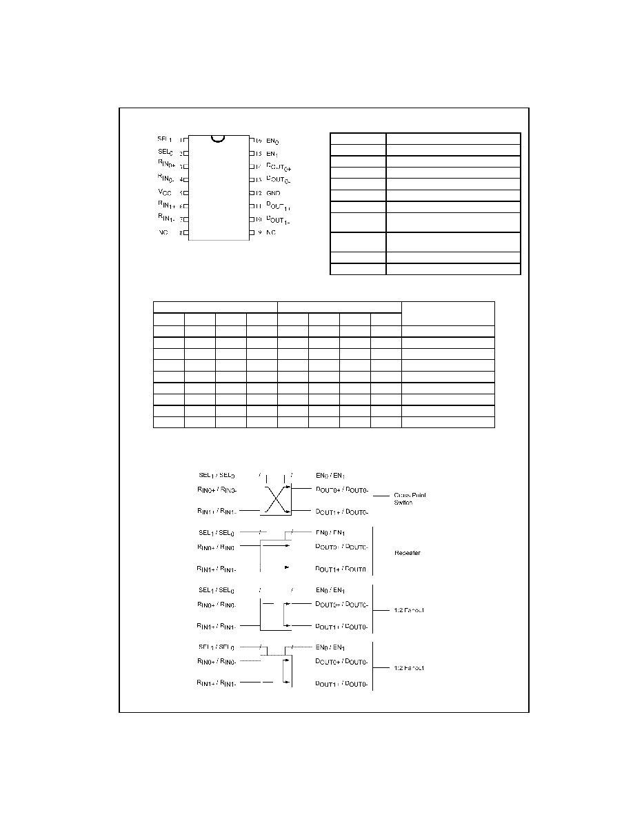
Connection Diagram
Pin Descriptions
Function Table
O
=
OPEN
L / O
=
LOW or OPEN
H
=
HIGH Logic Level
L
=
LOW Logic Level
X
=
Don't Care
Z
=
High Impedance
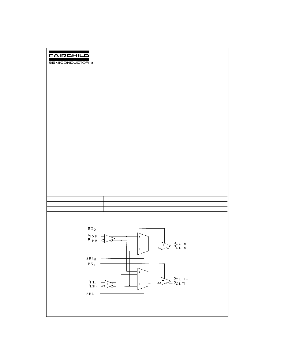
Function Diagrams
Pin Name
Description
R
IN0
+
, R
IN1
+
LVDS non-inverting data inputs
R
IN0
-
, R
IN1
-
LVDS inverting data inputs
D
OUT0
+
, D
OUT1
+
LVDS non-inverting data outputs
D
OUT0
-
, D
OUT1
-
LVDS inverting data outputs
EN
0
LVTTL input for enabling D
OUT0
+
/D
OUT0
-
EN
1
LVTTL input for enabling D
OUT1
+
/D
OUT1
-
SEL
0
LVTTL input for selecting R
IN0
+
/R
IN0
-
or
R
IN1
+
/R
IN1
-
for output D
OUT0
+
/D
OUT0
-
SEL
1
LVTTL input for selecting R
IN0
+
/R
IN0
-
or
R
IN1
+
/R
IN1
-
for output D
OUT1
+
/D
OUT1
-
V
CC
Power Supply
GND
Ground
Inputs
Outputs
Mode
SEL
0
SEL
1
EN
0
EN
1
D
OUT0
+
D
OUT0
-
D
OUT1
+
D
OUT1
-
L / O
L / O
H
H
R
IN0
+
R
IN0
-
R
IN0
+
R
IN0
-
1:2 Splitter
L / O
H
H
H
R
IN0
+
R
IN0
-
R
IN1
+
R
IN1
-
Repeater
H
L / O
H
H
R
IN1
+
R
IN1
-
R
IN0
+
R
IN0
-
Switch
H
H
H
H
R
IN1
+
R
IN1
-
R
IN1
+
R
IN1
-
1:2 Splitter
X
L / O
L / O
H
Z
Z
R
IN0
+
R
IN0
-
D
OUT0
Disabled
X
H
L / O
H
Z
Z
R
IN1
+
R
IN1
-
D
OUT0
Disabled
L / O
X
H
L / O
R
IN0
+
R
IN0
-
Z
Z
D
OUT1
Disabled
H
X
H
L / O
R
IN1
+
R
IN1
-
Z
Z
D
OUT1
Disabled
X
X
L / O
L / O
Z
Z
Z
Z
D
OUT0
and D
OUT1
Disabled
3
www.fairchildsemi.com
FI
N1022
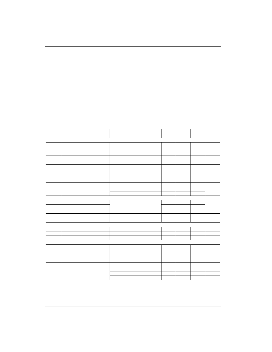
Absolute Maximum Ratings
(Note 1)
Recommended Operating
Conditions
Note 1: The "Absolute Maximum Ratings": are those values beyond which
damage to the device may occur. The databook specifications should be
met, without exception, to ensure that the system design is reliable over its
power supply, temperature and output/input loading variables. Fairchild
does not recommend operation of circuits outside databook specification.
DC Electrical Characteristics
Over supply voltage and operating temperature ranges, unless otherwise specified (Note 2)
Note 2: This part will only function with datasheet specification when a resistive load is applied to the driver outputs.
Note 3: All typical values are at T
A
=
25
°
C and with V
CC
=
3.3V.
Supply Voltage (V
CC
)
-
0.3V to
+
4.6V
DC Input Voltage (V
IN
)
-
0.3V to
+
4.6V
DC Output Voltage (V
OUT
)
-
0.3V to
+
4.6V
Driver Short Circuit Current (I
OSD
)
Continuous
Storage Temperature Range (T
STG
)
-
65
°
C to
+
150
°
C
Max Junction Temperature (T
J
)
150
°
C
Lead Temperature (T
L
)
(Soldering, 10 seconds)
260
°
C
Supply Voltage (V
CC
)
3.0V to 3.6V
Input Voltage (V
IN
)
0 to V
CC
Operating Temperature (T
A
)
-
40
°
C to
+
85
°
C
Electrostatic Discharge
(HBM 1.5 k
, 100 pF)
>
7500V
Electrostatic Discharge
(MM 0
, 100 pF)
>
300V
Symbol
Parameter
Test Conditions
Min
Typ
Max
Units
(Note 3)
LVDS Differential Driver Characteristics
V
OD
Output Differential Voltage
R
L
=
75
, See Figure 3
270
365
475
mV
R
L
=
75
, See Figure 3
285
365
440
T
A
=
25
°
C and V
CC
=
3.3V
V
OD
V
OD
Magnitude Change from
R
L
=
75
, See Figure 3
35
mV
Differential LOW-to-HIGH
V
OS
Offset Voltage
See Figure 3
1.0
1.2
1.45
V
V
OS
Offset Magnitude Change from
See Figure 3
35
mV
Differential LOW-to-HIGH
I
OZD
Disabled Output Leakage Current
V
OUT
=
3.6V or GND, Driver Disabled
±
10
µ
A
I
OFF
Power-Off Current
V
CC
=
0V, V
IN
or V
OUT
=
3.6V or 0V
±
20
µ
A
I
OS
Short Circuit Output Current
V
OUT
=
0V, Driver Enabled
-
10
mA
V
OUTx
+
=
0V, V
OUTx
-
=
0V, Driver Enabled
-
10
LVDS Differential Receiver Characteristics
V
TH
Differential Input Threshold HIGH
V
IC
=
0.05V or 1.2V or 3.25V
100
mV
V
TL
Differential Input Threshold LOW
V
CC
=
3.3V
-
100
V
IC
Input Common Mode Voltage
0.05
3.25
V
I
IND
Input Current (Differential Inputs)
V
IN
=
GND
±
20
µ
A
V
IN
=
V
CC
±
20
LVTTL Control Characteristics
V
IH
Input High Voltage
2
V
V
IL
Input Low Voltage
0.8
V
I
IN
Input Current
V
IN
=
3.6V or GND
±
20
µ
A
Device Characteristics
V
IK
Input Clamp Voltage
I
IK
=
-
18 mA
-
1.5
V
I
PU/PD
Output Power-Up/Power-Down
V
CC
=
0V to 1.5V
±
10
µ
A
High Z Leakage Current
C
IN
Input Capacitance
4.5
pF
C
OUT
Output Capacitance
4.5
pF
I
CC
Power Supply Current
No Load, All Drivers Enabled
35
mA
R
L
=
75
, All Drivers Enabled
35
mA
R
L
=
75
, All Drivers Enabled
35
mA
www.fairchildsemi.com
4
FIN1022
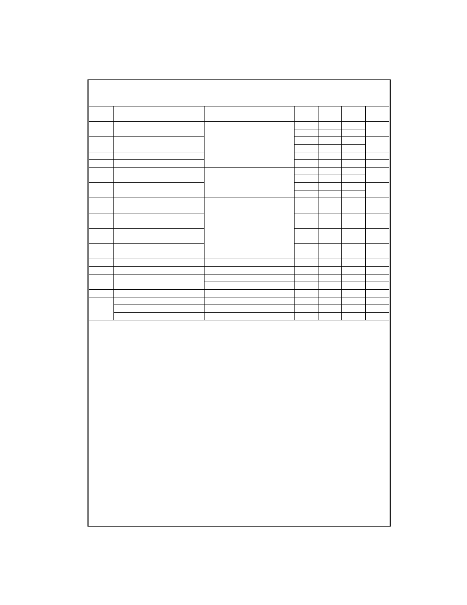
AC Electrical Characteristics
Over supply voltage and operating temperature ranges, unless otherwise specified
Note 4: All typical values are at T
A
=
25
°
C and with V
CC
=
3.3V.
Note 5: Part-to-part skew is the maximum delay time difference on like edges (LOW-to-HIGH or HIGH-to-LOW) for the same V
CC
and temperature condi-
tions.
Symbol
Parameter
Test Conditions
Min
Typ
Max
Units
(Note 4)
t
PLHD
Differential Output Propagation Delay
0.7
1.6
ns
LOW-to-HIGH
R
L
=
75
, C
L
=
5 pF,
1.0
1.2
1.3
t
PHLD
Differential Output Propagation Delay
V
CC
=
3.3V, T
A
=
25
°
C
0.7
1.6
ns
HIGH-to-LOW
See Figure 4 and Figure 5
1.0
1.2
1.3
t
TLHD
Differential Output Rise Time (20% to 80%)
290
580
ps
t
THLD
Differential Output Fall Time (80% to 20%)
290
580
ps
t
PLH
Selection Propagation Delay
0.6
1.5
ns
LOW-to-HIGH (SEL
n
to OUT
n
)
R
L
=
75
, C
L
=
5 pF,
0.9
1.1
1.2
t
PHL
Selection Propagation Delay
V
CC
=
3.3V, T
A
=
25
°
C
0.6
1.5
ns
HIGH-to-LOW (SEL
n
to OUT
n
)
See Figure 6 and Figure 7
0.9
1.1
1.2
t
ZHD
Differential Output Enable Time
3.5
ns
from Z-to-HIGH
t
ZLD
Differential Output Enable Time
3.5
ns
from Z-to-LOW
R
L
=
75
, C
L
=
5 pF
t
HZD
Differential Output Disable Time
See Figure 8 and Figure 9
3.5
ns
from HIGH-to-Z
t
LZD
Differential Output Disable Time
3.5
ns
from LOW-to-Z
t
SET
Input (IN
n
+
/IN
n
-
) Setup Time to SEL
n
See Figure 10
0.5
0.3
ns
t
HOLD
Input (IN
n
+
/IN
n
-
) Hold Time to SEL
n
See Figure 10
0.5
0.3
ns
t
JIT
Output Peak-to-Peak Jitter
2
23
-
1 PRBS Sequence at 800 Mbps
190
ps
50% Duty Cycle at 800 Mbps
20
35
ps
f
TOG
Maximum Toggle Frequency
R
L
=
75
, C
L
=
5 pF, See Figure 4
800
900
Mbps
t
SKEW
Within Device Channel-to-Channel Skew
35
80
ps
Pulse Skew |t
PLHD
-t
PHLD
|
0
225
ps
Part-to-Part Skew (Note 5)
100
500
ps
5
www.fairchildsemi.com
FI
N1022
Required Specifications
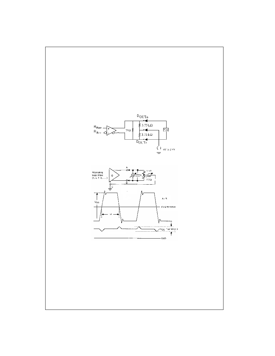
1. When the true and complement LVDS outputs (having
a 75
connected between outputs) are connected to
3.75 k
resistors and the common point of those 3.75
k
resistors are connected to a voltage source that
sweeps from 0 to 2.4V, the DC V
OD
and
V
OD
are still
maintained (see Figure 1).
2. When the true and complement LVDS outputs (having
a 5 pF capacitor attached between outputs) are con-
nected with 37.5
resistors each to common point,
then the common point does not vary by more than 150
mV under all process, temperature and voltage condi-
tions when the outputs switch either from LOW-to-
HIGH or from HIGH-to-LOW (see Figure 2).
3. Pull-down resistors are required on Enable (EN
0
and
EN
1
) and select (SEL
0
and SEL
1
) inputs.
4. Fail safe protection on the outputs that draw less than
20
µ
A of current (worst case) on the LVDS inputs. In
this condition, if the input is in fail safe selected to
OUT
0
+
/OUT
0
-
(say) and the outputs are Enabled then
OUT
0
+
=
HIGH and OUT
0
-
=
LOW. This prevents noise
from being amplified when the connection is broken.
5. In the disabled state the outputs can go beyond V
CC
but there should be no appreciable leakage (see I
OZD
and I
OFF
specifications)
FIGURE 1. Common Mode Supply Test Circuit
FIGURE 2. Dynamic V
OS
Test Circuit and Waveforms