 | ÐлекÑÑоннÑй компоненÑ: FIN1025 | СкаÑаÑÑ:  PDF PDF  ZIP ZIP |
Äîêóìåíòàöèÿ è îïèñàíèÿ www.docs.chipfind.ru
© 2002 Fairchild Semiconductor Corporation
DS500783
www.fairchildsemi.com
June 2002
Revised June 2002
FI
N1025
3.
3V L
V
DS 2-
Bit
Hi
gh Spe
e
d Di
ff
erent
i
al
D
r
ive
r
FIN1025
3.3V LVDS 2-Bit High Speed Differential Driver
General Description
This dual driver is designed for high speed interconnects
utilizing Low Voltage Differential Signaling (LVDS) technol-
ogy. The driver translates LVTTL signal levels to LVDS lev-
els with a typical differential output swing of 350mV which
provides low EMI at ultra low power dissipation even at
high frequencies. This device is ideal for high speed trans-
fer of clock and data.
The FIN1025 can be paired with its companion receiver,
the FIN1026, or any other LVDS receiver.
Features
s
Greater than 400Mbs data rate
s
Flow-through pinout simplifies PCB layout
s
3.3V power supply operation
s
0.4ns maximum differential pulse skew
s
1.7ns maximum propagation delay
s
Low power dissipation
s
Power-Off protection
s
Meets or exceeds the TIA/EIA-644 LVDS standard
s
14-Lead TSSOP package saves space
Ordering Code:
Devices also available in Tape and Reel. Specify by appending the suffix letter "X" to the ordering code.
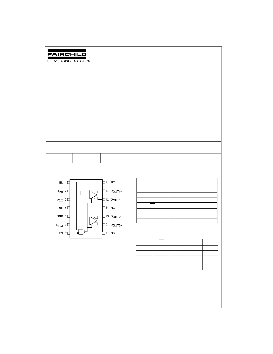
Connection Diagram
Pin Descriptions
Truth Table
H
=
HIGH Logic Level
L
=
LOW Logic Level
X
=
Don't Care
Z
=
High Impedance
Order Number
Package Number
Package Description
FIN1025MTC
MTC14
14-Lead Thin Shrink Small Outline Package (TSSOP), JEDEC MO-153, 4.4mm Wide
Pin Name
Description
D
IN1
, D
IN2
,
LVTTL Data Inputs
D
OUT1
+
, D
OUT2
+
Non-Inverting Driver Outputs
D
OUT1
-
, D
OUT2
-
Inverting Driver Outputs
EN
Driver Enable Pin
EN
Inverting Driver Enable Pin
V
CC
Power Supply
GND
Ground
NC
No Connect
Inputs
Outputs
EN
EN
D
IN
D
OUT
+
D
OUT
-
H
L or OPEN
H
H
L
H
L or OPEN
L
L
H
H
L or OPEN
OPEN
L
H
X
H
X
Z
Z
L or OPEN
X
X
Z
Z
www.fairchildsemi.com
2
FIN1025
Absolute Maximum Ratings
(Note 1)
Recommended Operating
Conditions
Note 1: The "Absolute Maximum Ratings": are those values beyond which
damage to the device may occur. The databook specifications should be
met, without exception, to ensure that the system design is reliable over its
power supply, temperature and output/input loading variables. Fairchild
does not recommend operation of circuits outside databook specification.
DC Electrical Characteristics
Over supply voltage and operating temperature ranges, unless otherwise specified
Note 2: All typical values are at T
A
=
25
°
C and with V
CC
=
3.3V.
Supply Voltage (V
CC
)
-
0.5V to
+
4.6V
LVTTL DC Input Voltage (V
IN
)
-
0.5V to
+
6V
LVDS DC Output Voltage (V
OUT
)
-
0.5V to 4.6V
Driver Short Circuit Current (I
OSD
)
Continuous
Storage Temperature Range (T
STG
)
-
65
°
C to
+
150
°
C
Max Junction Temperature (T
J
)
150
°
C
Lead Temperature (T
L
)
260
°
C
(Soldering, 10 seconds)
ESD (Human Body Model)
10,000V
ESD (Machine Model)
600V
Supply Voltage (V
CC
)
3.0V to 3.6V
Input Voltage (V
IN
)
0 to V
CC
Operating Temperature (T
A
)
-
40
°
C to
+
85
°
C
Symbol
Parameter
Test Conditions
Min
Typ
Max
Units
(Note 2)
V
OD
Output Differential Voltage
250
340
450
mV
V
OD
V
OD
Magnitude Change from
1.4
25
mV
Differential LOW-to-HIGH
R
L
=
100
, Driver Enabled,
V
OS
Offset Voltage
See Figure 1
1.125
1.25
1.375
V
V
OS
Offset Magnitude Change from
1.2
25
mV
Differential LOW-to-HIGH
V
OH
HIGH Output Voltage
V
IN
=
V
CC
, R
L
=
100
1.4
1.6
V
V
OL
LOW Output Voltage
V
IN
=
0V, R
L
=
100
0.9
1.05
V
I
OFF
Power Off Output Current
V
CC
=
0V, V
OUT
=
0V or 3.6V
-
20
20
µ
A
I
OS
Short Circuit Output Current
V
OUT
=
0V, Driver Enabled
-
3
-
6
mA
V
OD
=
0V, Driver Enabled
-
3.5
-
6
V
IH
Input HIGH Voltage
2.0
V
CC
V
V
IL
Input LOW Voltage
GND
0.8
V
I
IN
Input Current
V
IN
=
0V or V
CC
-
20
20
µ
A
I
OZ
Disabled Output Leakage Current
V
OUT
=
0V or 3.6V
-
20
20
µ
A
I
I(OFF)
Power-Off Input Current
V
CC
=
0V, V
IN
=
0V or 3.6V
-
20
20
µ
A
V
IK
Input Clamp Voltage
I
IK
=
-
18 mA
-
1.5
-
0.8
V
I
CC
Power Supply Current
No Load, V
IN
=
0V or V
CC
, Driver Enabled
5
8
mA
R
L
=
100
, Driver Disabled
1.7
4
R
L
=
100
, V
IN
=
0V or V
CC
, Driver Enabled
9
16
3
www.fairchildsemi.com
FI
N1025
AC Electrical Characteristics
Over supply voltage and operating temperature ranges, unless otherwise specified
Note 3: All typical values are at T
A
=
25
°
C and with V
CC
=
3.3V.
Note 4: t
SK(LH)
, t
SK(HL)
is the skew between specified outputs of a single device when the outputs have identical loads and are switching in the same direc-
tion.
Note 5: t
SK(PP)
is the magnitude of the difference in propagation delay times between any specified terminals of two devices switching in the same direction
(either LOW-to-HIGH or HIGH-to-LOW) when both devices operate with the same supply voltage, same temperature, and have identical test circuits.
Note 6: f
MAX
criteria: Input t
R
=
t
F
<
1ns, 0V to 3V, 50% Duty Cycle; Output V
OD
>
250 mv, 45% to 55% Duty Cycle; all switching in phase channels.
Note 7: Test Circuits in Figures 2, 4, 6 are simplified representations of test fixture and DUT loading.
Symbol
Parameter
Test Conditions
Min
Typ
Max
Units
(Note 3)
t
PLHD
Differential Propagation Delay
0.6
1.1
1.7
ns
LOW-to-HIGH
t
PHLD
Differential Propagation Delay
0.6
1.2
1.7
ns
HIGH-to-LOW
t
TLHD
Differential Output Rise Time (20% to 80%)
R
L
=
100
, C
L
=
10 pF,
0.4
1.2
ns
t
THLD
Differential Output Fall Time (80% to 20%)
See Figure 2 (Note 7), and Figure 3
0.4
1.2
ns
t
SK(P)
Pulse Skew |t
PLH
- t
PHL
|
0.4
ns
t
SK(LH)
Channel-to-Channel Skew
0.05
0.3
ns
t
SK(HL)
(Note 4)
t
SK(PP)
Part-to-Part Skew (Note 5)
1.0
ns
f
MAX
Maximum Frequency (Note 6)
R
L
=
100
, See Figure 6 (Note 7)
200
250
MHz
t
ZHD
Differential Output Enable Time from Z to HIGH
1.7
5.0
ns
t
ZLD
Differential Output Enable Time from Z to LOW
R
L
=
100
, C
L
=
10 pF,
1.7
5.0
ns
t
HZD
Differential Output Disable Time from HIGH to Z See Figure 4 (Note 7), and Figure 5
2.7
5.0
ns
t
LZD
Differential Output Disable Time from LOW to Z
2.7
5.0
ns
C
IN
Input Capacitance
4.2
pF
C
OUT
Output Capacitance
5.2
pF
www.fairchildsemi.com
4
FIN1025
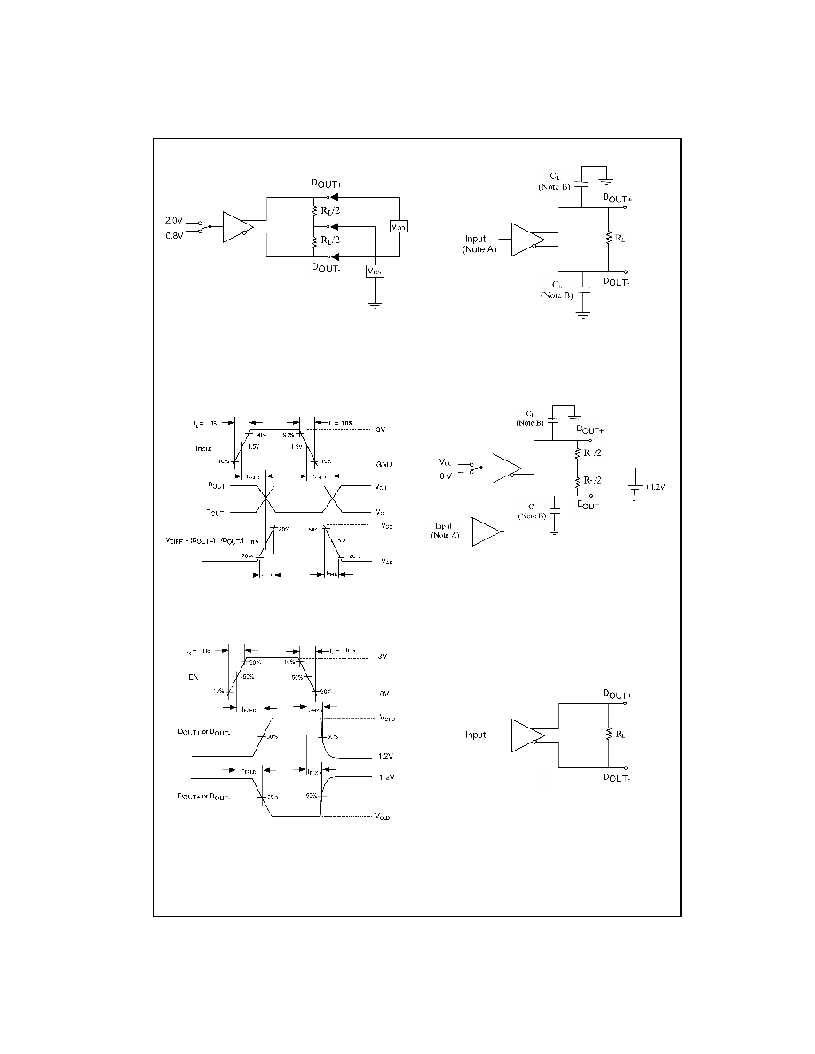
FIGURE 1. Differential Driver DC Test Circuit
Note A: All input pulses have frequency
=
10 MHz, t
R
or t
F
=
1 ns
Note B: C
L
includes all fixture and instrumentation capacitance
FIGURE 2. Differential Driver Propagation Delay and
Transition Time Test Circuit
FIGURE 3. AC Waveforms
Note B: All input pulses have the frequency
=
10 MHz, t
R
or t
F
=
1 ns
Note A: C
L
includes all fixture and instrumentation capacitance
FIGURE 4. Differential Driver Enable and
Disable Test Circuit
FIGURE 5. Enable and Disable AC Waveforms
FIGURE 6. f
MAX
Test Circuit
5
www.fairchildsemi.com
FI
N1025
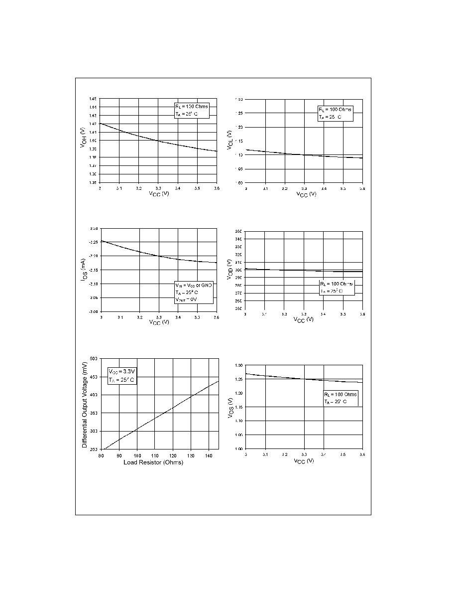
DC / AC Typical Performance Curves
FIGURE 7. Output High Voltage vs.
Power Supply Voltage
FIGURE 8. Output Low Voltage vs.
Power Supply Voltage
FIGURE 9. Output Short Circuit Current vs.
Power Supply Voltage
FIGURE 10. Differential Output Voltage vs.
Power Supply Voltage
FIGURE 11. Differential Output Voltage vs.
Load Resistor
FIGURE 12. Offset Voltage vs.
Power Supply Voltage