 | ÐлекÑÑоннÑй компоненÑ: FIN1028M | СкаÑаÑÑ:  PDF PDF  ZIP ZIP |
Äîêóìåíòàöèÿ è îïèñàíèÿ www.docs.chipfind.ru
© 2003 Fairchild Semiconductor Corporation
DS500503
www.fairchildsemi.com
March 2001
Revised June 2003
FI
N1028
3.
3V L
V
DS 2-
Bit
Hi
gh Spe
e
d Di
ff
erent
i
al
R
e
ceiver
FIN1028
3.3V LVDS 2-Bit High Speed Differential Receiver
General Description
This dual receiver is designed for high speed interconnects
utilizing Low Voltage Differential Signaling (LVDS) technol-
ogy. The receiver translates LVDS levels, with a typical dif-
ferential input threshold of 100 mV, to LVTTL signal levels.
LVDS provides low EMI at ultra low power dissipation even
at high frequencies. This device is ideal for high speed
transfer of clock and data.
The FIN1028 can be paired with its companion driver, the
FIN1027, or any other LVDS driver.
Features
s
Greater than 400Mbs data rate
s
3.3V power supply operation
s
0.4ns maximum differential pulse skew
s
2.5ns maximum propagation delay
s
Low power dissipation
s
Power-Off protection
s
Fail safe protection for open-circuit, shorted and
terminated conditions
s
Meets or exceeds the TIA/EIA-644 LVDS standard
s
Flow-through pinout simplifies PCB layout
s
8-Lead SOIC and 8-terminal MLP packages save space
Ordering Code:
Note 1: Devices also available in Tape and Reel. Specify by appending the suffix letter "X" to the ordering code.
Pin Descriptions
Function Table
H
=
HIGH Logic Level
L
=
LOW Logic Level
Fail Safe
=
Open, Shorted, Terminated
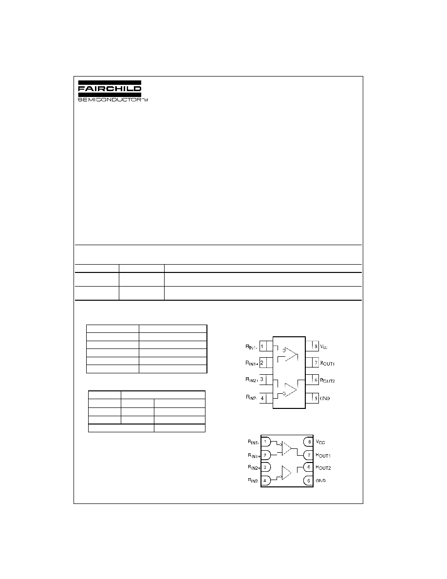
Connection Diagrams
Pin Assignment for SOIC
(Top View)
Terminal Assignments for MLP
(Top Through View)
Order Number
Package Number
Package Description
FIN1028M
(Note 1)
M08A
8-Lead Small Outline Integrated Circuit (SOIC), JEDEC MS-012, 0.150" Narrow
FIN1028MPX
(Preliminary)
MLP08C
8-Terminal Molded Leadless Package (MLP) Dual, JEDEC MO-229, 2mm Square
[TAPE and REEL]
Pin Name
Description
R
OUT1
, R
OUT2
LVTTL Data Outputs
R
IN1
+
, R
IN2
+
Non-inverting LVDS Inputs
R
IN1
-
, R
IN2
-
Inverting LVDS Inputs
V
CC
Power Supply
GND
Ground
Input
Outputs
R
IN
+
R
IN
+
R
OUT
L
H
L
H
L
H
Fail Safe Condition
H
www.fairchildsemi.com
2
FIN1028
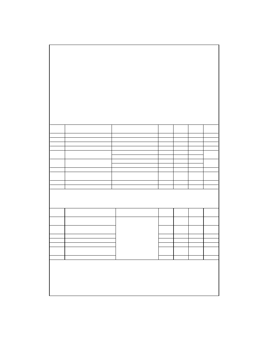
Absolute Maximum Ratings
(Note 2)
Recommended Operating
Conditions
Note 2: The "Absolute Maximum Ratings": are those values beyond which
damage to the device may occur. The databook specifications should be
met, without exception, to ensure that the system design is reliable over its
power supply, temperature and output/input loading variables. Fairchild
does not recommend operation of circuits outside databook specification.
DC Electrical Characteristics
Over supply voltage and operating temperature ranges, unless otherwise specified
Note 3: All typical values are at T
A
=
25
°
C and with V
CC
=
3.3V.
AC Electrical Characteristics
Over supply voltage and operating temperature ranges, unless otherwise specified
Note 4: All typical values are at T
A
=
25
°
C and with V
CC
=
3.3V.
Note 5: t
SK(LH)
, t
SK(HL)
is the skew between specified outputs of a single device when the outputs have identical loads and are switching in the same direc-
tion.
Note 6: t
SK(PP)
is the magnitude of the difference in propagation delay times between any specified terminals of two devices switching in the same direction
(either LOW-to-HIGH or HIGH-to-LOW) when both devices operate with the same supply voltage, same temperature, and have identical test circuits.
Supply Voltage (V
CC
)
-
0.5V to
+
4.6V
DC Input Voltage (R
INx
+
, R
INx
-
)
-
0.5V to
+
4.7V
DC Output Voltage (R
OUTx
)
-
0.5V to
+
6V
DC Output Current (I
O
)
16 mA
Storage Temperature Range (T
STG
)
-
65
°
C to
+
150
°
C
Max Junction Temperature (T
J
)
150
°
C
Lead Temperature (T
L
)
(Soldering, 10 seconds)
260
°
C
ESD (Human Body Model)
6500V
ESD (Machine Model)
300V
Supply Voltage (V
CC
)
3.0V to 3.6V
Input Voltage (V
IN
)
0 to V
CC
Magnitude of Differential Voltage
(|V
ID
|)
100 mV to V
CC
Common-mode Input Voltage
(V
IC
)
0.05V to 2.35V
Operating Temperature (T
A
)
-
40
°
C to
+
85
°
C
Symbol
Parameter
Test Conditions
Min
Typ
Max
Units
(Note 3)
V
TH
Differential Input Threshold HIGH
See Figure 1 and Table 1
100
mV
V
TL
Differential Input Threshold LOW
See Figure 1 and Table 1
-
100
mV
I
IN
Input Current
V
IN
=
0V or V
CC
±
20
µ
A
I
I(OFF)
Power-OFF Input Current
V
CC
=
0V, V
IN
=
0V or 3.6V
±
20
µ
A
V
OH
Output HIGH Voltage
I
OH
=
-
100
µ
A
V
CC
-
0.2
V
I
OH
=
-
8 mA
2.4
V
OL
Output LOW Voltage
I
OH
=
100
µ
A
0.2
V
I
OL
=
8 mA
0.5
V
IK
Input Clamp Voltage
I
IK
=
-
18 mA
-
1.5
V
I
CC
Power Supply Current
(R
IN
+
=
1V and R
IN
-
=
1.4V) or
9
mA
(R
IN
+
=
1.4V and R
IN
-
=
1V)
C
IN
Input Capacitance
4
pF
C
OUT
Output Capacitance
6
pF
Symbol
Parameter
Test Conditions
Min
Typ
Max
Units
(Note 4)
t
PLH
Differential Propagation Delay
0.9
2.5
ns
LOW-to-HIGH
t
PHL
Differential Propagation Delay
0.9
2.5
ns
HIGH-to-LOW
t
TLH
Output Rise Time (20% to 80%)
|V
ID
|
=
400 mV, C
L
=
10 pF,
0.5
ns
t
THL
Output Fall Time (80% to 20%)
See Figure 1 and Figure 2
0.5
ns
t
SK(P)
Pulse Skew |t
PLH
- t
PHL
|
0.4
ns
t
SK(LH)
,
Channel-to-Channel Skew
0.3
ns
t
SK(HL)
(Note 5)
t
SK(PP)
Part-to-Part Skew (Note 6)
1.0
ns
3
www.fairchildsemi.com
FI
N1028
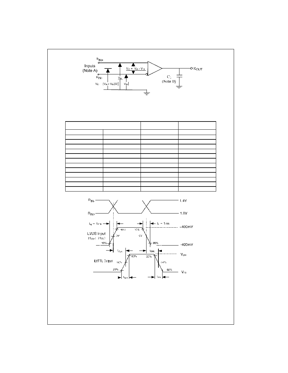
Note A: All input pulses have frequency
=
10 MHz, t
R
or t
F
=
1 ns
Note B: C
L
includes all probe and fixture capacitances
FIGURE 1. Differential Driver Propagation Delay and Transition Time Test Circuit
TABLE 1. Receiver Minimum and Maximum Input Threshold Test Voltages
FIGURE 2. AC Waveforms
Applied Voltages (V)
Resulting Differential
Input Voltage (mV)
Resulting Common Mode
Input Voltage (V)
V
IA
V
IB
V
ID
V
IC
1.25
1.15
100
1.2
1.15
1.25
-
100
1.2
2.4
2.3
100
2.35
2.3
2.4
-
100
2.35
0.1
0
100
0.05
0
0.1
-
100
0.05
1.5
0.9
600
1.2
0.9
1.5
-
600
1.2
2.4
1.8
600
2.1
1.8
2.4
-
600
2.1
0.6
0
600
0.3
0
0.6
-
600
0.3
www.fairchildsemi.com
4
FIN1028
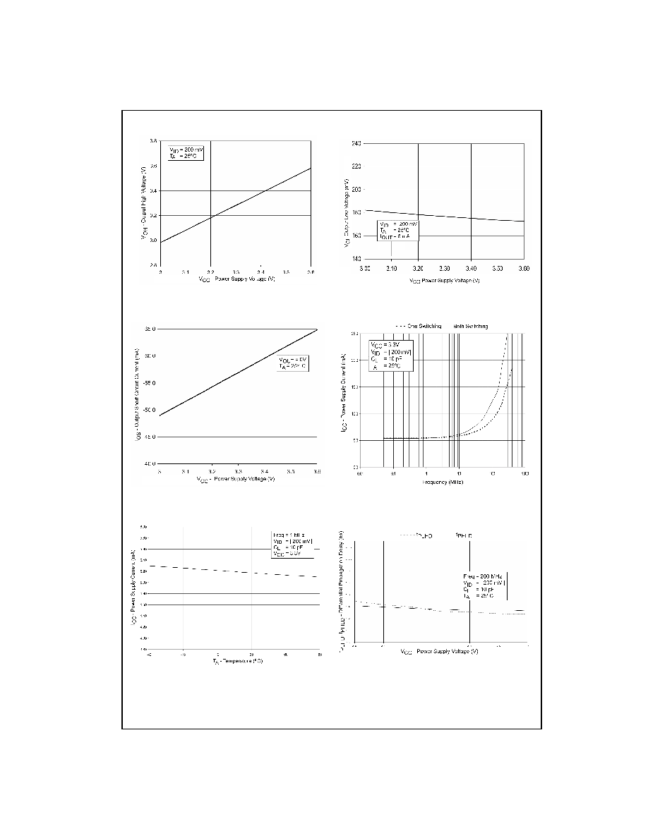
DC /AC Typical Performance Curves
FIGURE 3. Output High Voltage vs.
Power Supply Voltage
FIGURE 4. Output Low Voltage vs.
Power Supply Voltage
FIGURE 5. Output Short Circuit Current vs.
Power Supply Voltage
FIGURE 6. Power Supply Current vs.
Frequency
FIGURE 7. Power Supply Current vs.
Ambient Temperature
FIGURE 8. Differential Propagation Delay vs.
Power Supply Voltage
5
www.fairchildsemi.com
FI
N1028
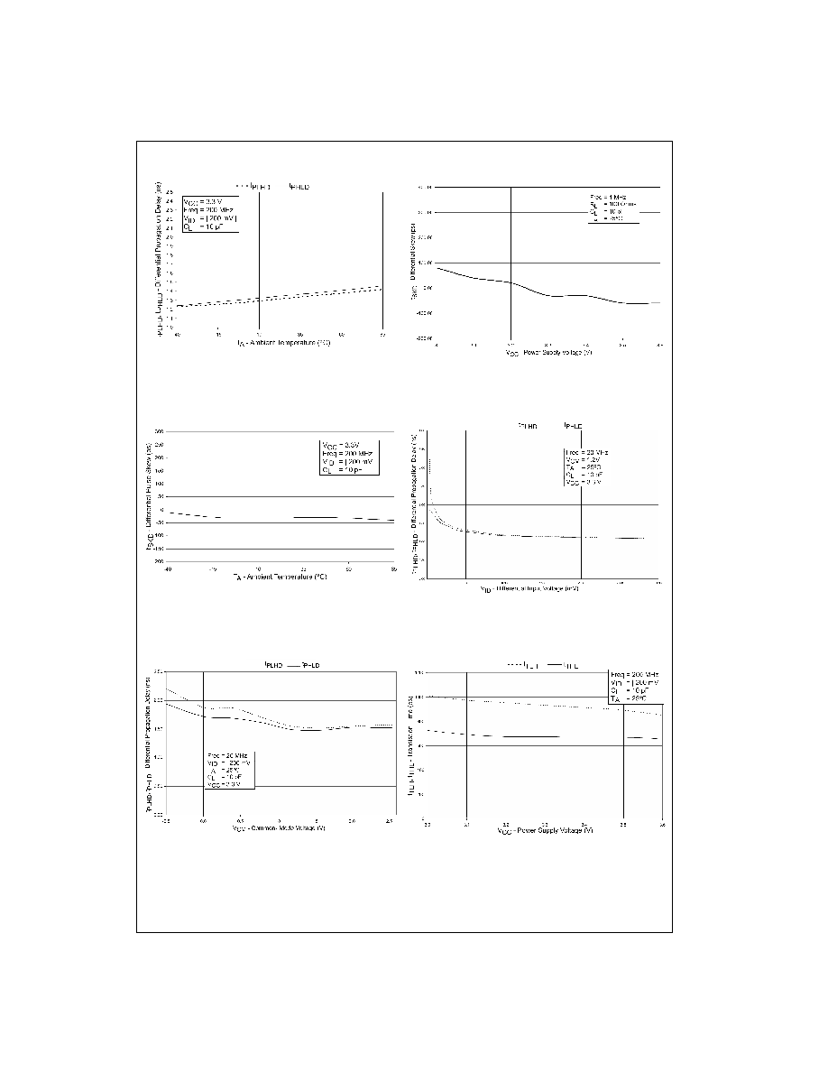
DC /AC Typical Performance Curves
(Continued)
FIGURE 9. Differential Propagation Delay vs.
Ambient Temperature
FIGURE 10. Differential Skew (t
PLH
- t
PHL
) vs.
Power Supply Voltage
FIGURE 11. Differential Skew (t
PHL
- t
PHL
) vs.
Ambient Temperature
FIGURE 12. Differential Propagation Delay vs.
Differential Input Voltage
FIGURE 13. Differential Propagation Delay vs.
Common-Mode Voltage
FIGURE 14. Transition Time vs.
Power Supply Voltage