 | –≠–ª–µ–∫—Ç—Ä–æ–Ω–Ω—ã–π –∫–æ–º–ø–æ–Ω–µ–Ω—Ç: FIN1049 | –°–∫–∞—á–∞—Ç—å:  PDF PDF  ZIP ZIP |

© 2003 Fairchild Semiconductor Corporation
DS500846
www.fairchildsemi.com
March 2003
Revised March 2003
FI
N1049 L
V
DS
Dual
Li
ne
Dr
iver
wi
th Dual Li
ne
Recei
ver
FIN1049
LVDS Dual Line Driver with Dual Line Receiver
General Description
This dual Driver-Receiver is designed for high speed inter-
connects utilizing Low Voltage Differential Signaling
(LVDS) technology. The Driver accepts LVTTL inputs and
translates them to LVDS outputs. The Receiver accepts
LVDS inputs and translates them to LVTTL outputs. The
LVDS levels have a typical differential output swing of
350mV which provide for low EMI at ultra low power dissi-
pation even at high frequencies. The FIN1049 can accept
LVPECL inputs for translating from LVPECL to LVDS. The
En and Enb inputs are ANDed together to enable/disable
the outputs. The enables are common to all four outputs. A
single line driver and single line receiver function is also
available in the FIN1019.
Features
s
Greater than 400 Mbps data rate
s
3.3V power supply operation
s
Low power dissipation
s
Fail safe protection for open-circuit conditions
s
Meets or exceeds the TIA/EIA-644-A LVDS standard
s
16-pin TSSOP package saves space
s
Flow-through pinout simplifies PCB layout
s
Enable/Disable for all outputs
s
Industrial operating temperature range:
-
40
∞
C to
+
85
∞
C
Ordering Code:
Device also available in Tape and Reel. Specify by appending suffix letter "X" to the ordering code.
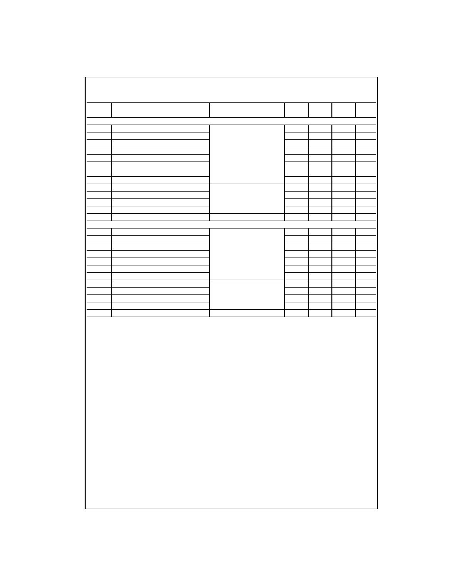
Pin Descriptions
Connection Diagram
Order Number
Package Number
Package Description
FIN1049MTC
MTC16
16-Lead Thin Shrink Small Outline Package (TSSOP), JEDEC MO-153, 4.4mm Wide
Pin Name
Description
R
IN1
+
, R
IN2
+
Non-Inverting LVDS Inputs
R
IN1
-
, R
IN2
-
Inverting LVDS Inputs
D
OUT1
+
, D
OUT2
+
Non-Inverting Driver Outputs
D
OUT1
-
, D
OUT2
-
Inverting Driver Outputs
EN, ENb
Driver Enable Pins for All Outputs
R
OUT1
, R
OUT2
LVTTL Output Pins for R
OUT1
and R
OUT2
D
IN2
, D
IN2
LVTTL Input Pins for D
IN1
and D
IN2
V
CC
Power Supply (3.3V)
GND
Ground

www.fairchildsemi.com
2
FIN1049
Function Table
H
=
HIGH Logic Level
L
=
LOW Logic Level or OPEN
X
=
Don't Care
Z
=
High Impedance
Note 1: Any unused Receiver Inputs should be left Open.
Functional Diagram
Inputs
Outputs (LVTTL)
Inputs (LVDS) (Note 1)
Outputs (LVDS)
EN
ENb
R
OUT1
R
OUT2
R
IN#
+
R
IN#
-
D
OUT#
+
D
OUT#
-
H
L
ON
ON
ON
ON
H
H
Z
Z
Z
Z
L
H
Z
Z
Z
Z
L
L
Z
Z
Z
Z
H
L
H
H
Open Current
Fail Safe Condition

3
www.fairchildsemi.com
FI
N1049
Absolute Maximum Ratings
(Note 2)
Recommended Operating
Conditions
Note 2: The "Absolute Maximum Ratings": are those values beyond which
damage to the device may occur. The databook specifications should be
met, without exception, to ensure that the system design is reliable over its
power supply, temperature and output/input loading variables. Fairchild
does not recommend operation of circuits outside databook specification.
DC Electrical Characteristics
Over supply voltage and operating temperature ranges, unless otherwise specified
Note 3: All typical values are at T
A
=
25
∞
C and with V
CC
=
3.3V.
Note 4: Both driver and receiver inputs are static. All LVDS outputs have 100
load. None of the outputs have any lumped capacitive load.
Supply Voltage (V
CC
)
-
0.5V to
+
4.6V
LVDS DC Input Voltage (V
IN
)
-
0.5V to
+
4.6V
LVDS DC Output Voltage (V
OUT
)
-
0.5V to
+
4.6V
Driver Short Circuit Current (I
OSD
)
Continuous 10mA
Storage Temperature Range (T
STG
)
-
65
∞
C to
+
150
∞
C
Max Junction Temperature (T
J
)
150
∞
C
Lead Temperature (T
L
)
(Soldering, 10 seconds)
260
∞
C
ESD (Human Body Model)
>
7000V
ESD (Machine Model)
>
250V
Supply Voltage (V
CC
)
3.0V to 3.6V
Magnitude of Differential Voltage
(|V
ID
|)
100mV to V
CC
Operating Temperature (T
A
)
-
40
∞
C to
+
85
∞
C
Symbol
Parameter
Test Conditions
Min
Typ
Max
Units
(Note 3)
LVDS Input DC Specifications (R
IN1
+
, R
IN1
-
, R
IN2
+
, R
IN2
-
) See Figure 1 and Table 1
V
TH
Differential Input Threshold HIGH
VCM
=
1.2V, 0.05V, 2.35V
0.0
35.0
mV
V
TL
Differential Input Threshold LOW
-
100
0.0
mV
V
IC
Common Mode Voltage Range
V
ID
=
100mV, V
CC
=
3.3V
V
ID
/2
V
CC
-
(V
ID
/2)
V
I
IN
Input Current
V
CC
=
0V or 3.6V, V
IN
=
0V or 2.8V
±
20.0
mA
CMOS/ LVTTL Input DC Specifications (EN, ENb, D
IN1
, D
IN2
)
V
IH
Input High Voltage (LVTTL)
2.0
V
CC
V
V
IL
Input Low Voltage (LVTTL)
GND
0.8
V
I
IN
Input Current
V
IN
=
0V or V
CC
±
20.0
µ
A
(EN, ENb, D
IN1
, D
IN2
, R
INx
+
, and
R
INx
-
)
V
IK
Input Clamp Voltage
V
IK
=
-
18mA
-
1.5
-
0.7
V
LVDS Output DC Specifications (D
OUT1
+
, D
OUT1
-
, D
OUT2
+
, D
OUT2
-
)
V
OD
Output Differential Voltage
250
350
450
mV
V
OD
V
OD
Magnitude Change from
R
L
=
100
,
35.0
mV
Differential LOW-to-HIGH
Driver Enabled,
V
OS
Offset Voltage
See Figure 2
1.125
1.25
1.375
V
V
OS
Offset Magnitude Change from
25.0
mV
Differential LOW-to-HIGH
I
OS
Short Circuit Output Current
D
OUT
+
=
0V & D
OUT
-
=
0V, Driver Enabled
-
9.0
mA
I
OSD
V
OD
=
0V, Driver Enabled
-
9.0
mA
I
OFF
Power-Off Input or Output Current
V
CC
=
0V, V
OUT
=
0V or V
CC
±
20.0
µ
A
I
OZD
Disabled Output Leakage Current
Driver Disabled, D
OUT
+
=
0V or V
CC
±
10.0
µ
A
or D
OUT
-
=
0V or V
CC
CMOS/LVTTL Output DC Specifications (R
OUT1
, R
OUT2
)
V
OH
Output High Voltage
I
OH
=
-
2mA, V
ID
=
200mV
2.7
V
V
OL
Output Low Voltage
I
OL
=
2mA, V
ID
=
200mV
0.250
V
I
OZ
Disabled Output Leakage Current
Driver Disabled, R
OUTn
=
0V or V
CC
±
10.0
µ
A
I
CC
Power Supply Current (Note 4)
Drivers Enabled, Any Valid Input Condition
25.0
mA
I
CCZ
Power Supply Current
Drivers Disabled
10.0
mA
C
IND
Input Capacitance
LVDS Input
3.0
pF
C
OUT
Output Capacitance
LVDS Output
4.0
pF
C
INT
Input Capacitance
LVTTL Input
3.5
pF
www.fairchildsemi.com
4
FIN1049
AC Electrical Characteristics
Over supply voltage and operating temperature ranges, unless otherwise specified
Note 5: All typical values are at T
A
=
25
∞
C and with V
CC
=
3.3V.
Note 6: t
SK(LH)
, t
SK(HL)
is the skew between specified outputs of a single device when the outputs have identical loads and are switching in the same
direction.
Note 7: t
SK(PP)
is the magnitude of the difference in propagation delay times between any specified terminals of two devices switching in the same direction
(either LOW-to-HIGH or HIGH-to-LOW) when both devices operate with the same supply voltage, same temperature, and have identical test circuits.
Note 8: f
MAX
generator input conditions: t
r
=
t
f
<
1ns (10% to 90%), 50% duty cycle, 0V to 3V. Output criteria: duty cycle
=
45% / 55%, V
OD
>
250mV, all chan-
nels switch.
Note 9: f
MAXT
generator input conditions: t
r
=
t
f
<
1ns (10% to 90%), 50% duty cycle, V
ID
=
200mV, V
CM
=
1.2V. Output criteria: duty cycle
=
45% / 55%, V
OH
>
2.7V. V
OL
<
0.25V, all channels switching.
Symbol
Parameter
Test Conditions
Min
Typ
Max
Units
(Note 5)
Switching Characteristics - LVDS Outputs
t
PLHD
Differential Propagation Delay LOW-to-HIGH
See Figures 3, 4
2.0
ns
t
PHLD
Differential Propagation Delay HIGH-to-LOW
2.0
ns
t
TLHD
Differential Output Rise Time (20% to 80%)
0.2
1.0
ns
t
THLD
Differential Output Fall Time (80% to 20%)
0.2
1.0
ns
t
SK(P)
Pulse Skew |t
PLH
- t
PHL
|
0.35
ns
t
SK(LH)
,
Channel-to-Channel Skew (Note 6)
0.35
ns
t
SK(HL)
t
SK(PP)
Part-to-Part Skew (Note 7)
1.0
ns
t
PZHD
Differential Output Enable Time from Z-to-HIGH
See Figures 5, 6
6.0
ns
t
PZLD
Differential Output Enable Time from A-to-LOW
6.0
ns
t
PHZD
Differential Output Disable Time from HIGH-to-Z
3.0
ns
t
PLZD
Differential Output Disable Time from LOW-to-Z
3.0
ns
f
MAXD
Maximum Frequency (Note 8)
See Figure 3
200
MHz
Switching Characteristics - LVTTL Outputs
t
PHL
Propagation Delay HIGH-to-LOW
Measured from 20% to 80% signal
0.5
1.0
3.5
ns
t
PLH
Propagation Delay LOW-to-HIGH
V
ID
=
200mV;
0.5
1.0
3.5
ns
t
SK1
Pulse Skew
Distributed Load
0.0
35.0
400
ps
t
SK2
Channel-to-Channel Skew
C
L
=
15pF and 50
;
0.0
50.0
500
ps
t
SK3
Part-to-Part Skew
R
L
=
1K
; 0.0
1.0
ns
t
LHR
Transition Time LOW-to-HIGH
V
OS
=
1.2V;
0.1
0.25
1.4
ns
t
HLR
Transition Time HIGH-to-LOW
See Figures 7, 8
0.1
0.18
1.4
ns
t
PHZ
Disable Time HIGH-to-Z
See Figures 9, 10
2.2
4.5
8.0
ns
t
PLZ
Disable Time LOW-to-Z
1.3
3.5
8.0
ns
t
PZH
Enable Time Z-to-HIGH
1.8
3.0
7.0
ns
t
PZL
Enable Time Z-to-LOW
0.9
1.4
7.0
ns
f
MAXT
Maximum Frequency (Note 9)
See Figure 7
200
MHz
5
www.fairchildsemi.com
FI
N1049
Required Specifications
1. Human Body Model ESD and Machine Model ESD
should be measured using MIL-STD-883C method
3015.7 standard.
2. Latch-up immunity should be tested to the EIA/JEDEC
Standard Number 78 (EIA/JESD78).
Note: C
L
=
15pF, includes all probe and jig capacitances
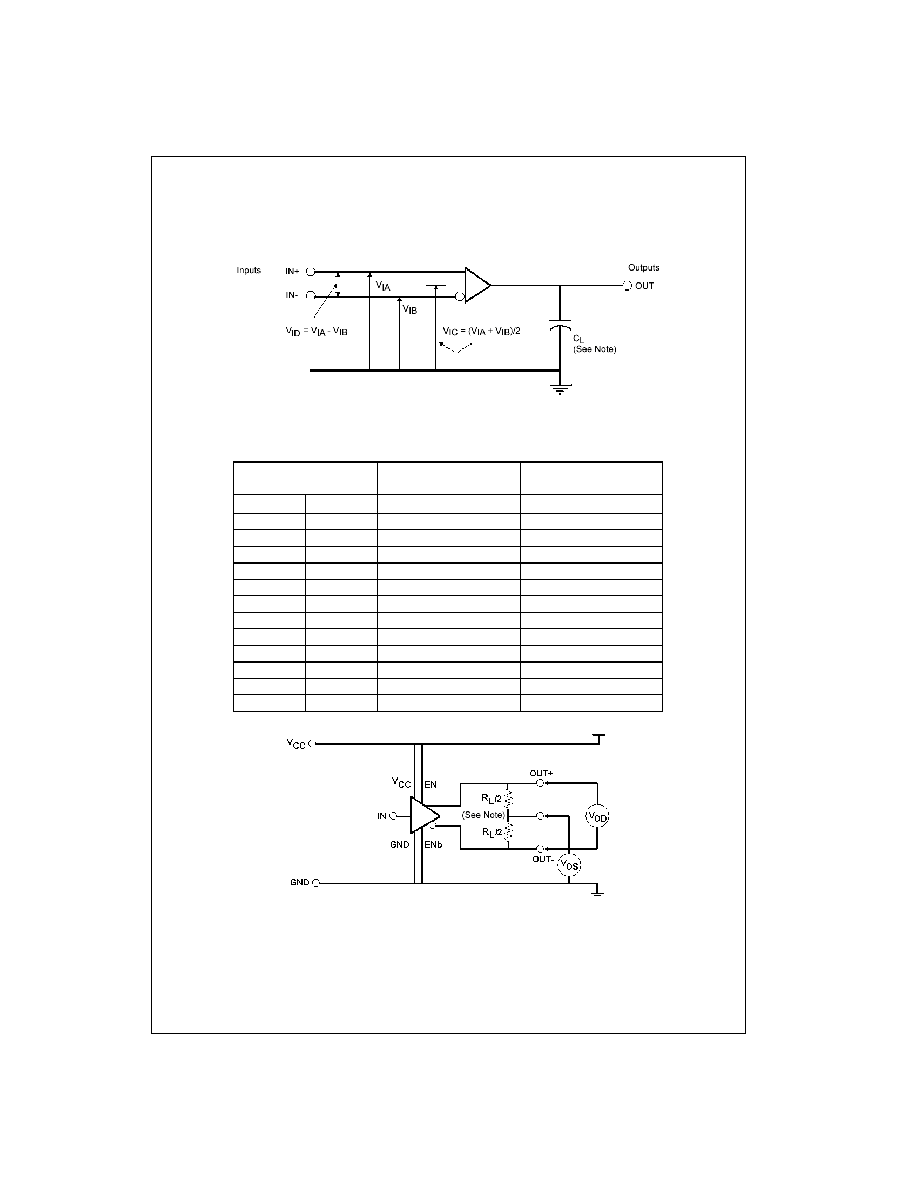
FIGURE 1. Differential Receiver Voltage Definitions Test Circuit
TABLE 1. Receiver Minimum and Maximum Input Threshold Test Voltages
Note: R
L
=
100
FIGURE 2. LVDS Output Circuit for DC Test
Applied Voltages (V)
Resulting Differential Input
Resulting Common
Voltage (mV)
Mode Input Voltage (V)
V
IA
V
IB
V
ID
V
IC
1.25
1.15
100
1.2
1.15
1.25
-
100
1.2
V
CC
V
CC
- 0.1
100
V
CC
- 0.05
V
CC
- 0.1
V
CC
-
100
V
CC
- 0.05
0.1
0.0
100
0.05
0.0
0.1
-
100
0.05
1.75
0.65
1100
1.2
0.65
1.75
-
1100
1.2
V
CC
V
CC
- 1.1
1100
V
CC
- 0.55
V
CC
- 1.1
V
CC
-
1100
V
CC
- 0.55
1.1
0.0
1100
0.55
0.0
1.1
-
1100
0.55