 | ÐлекÑÑоннÑй компоненÑ: FIN1101 | СкаÑаÑÑ:  PDF PDF  ZIP ZIP |
Äîêóìåíòàöèÿ è îïèñàíèÿ www.docs.chipfind.ru
© 2002 Fairchild Semiconductor Corporation
DS500654
www.fairchildsemi.com
January 2002
Revised September 2002
FI
N1
101 L
V
DS
Si
ngle Port
Hi
gh
Spee
d
Repeat
er
FIN1101
LVDS Single Port High Speed Repeater
General Description
This single port repeater is designed for high speed inter-
connects utilizing Low Voltage Differential Signaling
(LVDS) technology. It accepts and outputs LVDS levels
with a typical differential output swing of 330 mV which pro-
vides low EMI at ultra low power dissipation even at high
frequencies. It can directly accept multiple differential I/O
including: LVPECL, HSTL, and SSTL-2 for translating
directly to LVDS.
Features
s
Up to 1.6 Gb/s full differential path
s
3.5 ps max random jitter and 135 ps max deterministic
jitter
s
3.3V power supply operation
s
Wide rail-to-rail common mode range
s
Ultra low power consumption
s
LVDS receiver inputs accept LVPECL, HSTL, and
SSTL-2 directly
s
Power off protection
s
7 kV HBM ESD protection (all pins)
s
Meets or exceed the TA/EIA-644-A LVDS standard
s
Packaged in 8-pin SOIC and US8
s
Open circuit fail safe protection
Ordering Code:
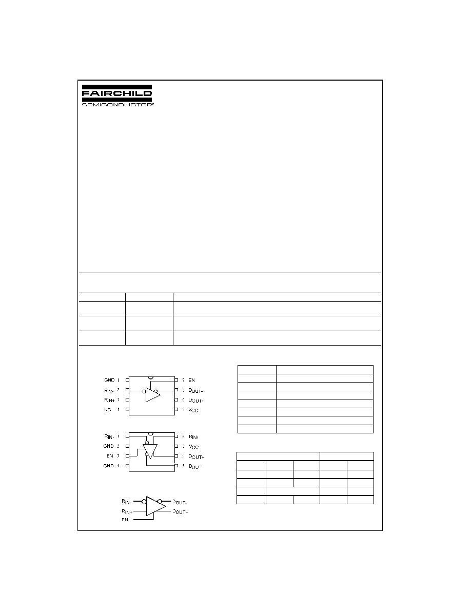
Connection Diagrams
SOIC Package
US8 Package
Functional Diagram
Pin Descriptions
Function Table
H
=
HIGH Logic Level
L
=
LOW Logic Level
X
=
Don't Care
Z
=
High Impedance
Order Number
Package Number
Package Description
FIN1101M
M08A
8-Lead Small Outline Integrated Circuit (SOIC), JEDEC MS-012, 0.150" Narrow
[TUBE]
FIN1101MX
M08A
8-Lead Small Outline Integrated Circuit (SOIC), JEDEC MS-012, 0.150" Narrow
[TAPE and REEL]
FIN1101K8X
MAB08A
8-Lead US8, JEDEC MO-187, Variation CA 3.1mm Wide
[TAPE and REEL]
Pin Name
Description
R
IN
+
Non-Inverting LVDS Inputs
R
IN
-
Inverting LVDS Inputs
D
OUT
+
Non-Inverting Driver Outputs
D
OUT
-
Inverting Driver Outputs
EN
Driver Enable Pin
V
CC
Power Supply
GND
Ground
Inputs
Outputs
EN
R
IN
+
R
IN
-
D
OUT
+
D
OUT
-
H
H
L
H
L
H
L
H
L
H
H
Fail Safe Case
H
L
L
X
X
Z
Z
www.fairchildsemi.com
2
FIN1
101
Absolute Maximum Ratings
(Note 1)
Recommended Operating
Conditions
Note 1: The "Absolute Maximum Ratings": are those values beyond which
damage to the device may occur. The databook specifications should be
met, without exception, to ensure that the system design is reliable over its
power supply, temperature and output/input loading variables. Fairchild
does not recommend operation of circuits outside databook specification.
DC Electrical Characteristics
Over supply voltage and operating temperature ranges, unless otherwise specified
Note 2: All typical values are at T
A
=
25
°
C and with V
CC
=
3.3V.
Supply Voltage (V
CC
)
-
0.5V to
+
4.6V
LVDS DC Input Voltage (V
IN
)
-
0.5V to
+
4.6V
LVDS DC Output Voltage (V
OUT
)
-
0.5V to
+
4.6V
Driver Short Circuit Current (I
OSD
)
Continuous 10 mA
Storage Temperature Range (T
STG
)
-
65
°
C to
+
150
°
C
Max Junction Temperature (T
J
)
150
°
C
Lead Temperature (T
L
)
(Soldering, 10 seconds)
260
°
C
ESD (Human Body Model)
7000V
ESD (Machine Model)
300V
Supply Voltage (V
CC
)
3.0V to 3.6V
Operating Temperature (T
A
)
-
40
°
C to
+
85
°
C
Magnitude of Input
Differential Voltage (|V
ID
|)
100 mV to V
CC
Common Mode Input Voltage
(V
IC
)
(0V
+
|V
ID
|/2) to (V
CC
-
|V
ID
|/2)
Symbol
Parameter
Test Conditions
Min
Typ
Max
Units
(Note 2)
V
TH
Differential Input Threshold HIGH
See Figure 1; V
IC
=
+
0.05V,
+
1.2V, or (V
CC
-
0.05V)
100
mV
V
TL
Differential Input Threshold LOW
See Figure 1; V
IC
=
+
0.05V,
+
1.2V, or (V
CC
-
0.05V)
-
100
mV
V
IH
Input High Voltage (EN)
2.0
V
CC
V
V
IL
Input Low Voltage (EN)
GND
0.8
V
V
OD
Output Differential Voltage
250
330
450
mV
V
OD
V
OD
Magnitude Change from
R
L
=
100
, Driver Enabled,
25
mV
Differential LOW-to-HIGH
See Figure 2
V
OS
Offset Voltage
1.125
1.23
1.375
V
V
OS
Offset Magnitude Change from
25
mV
Differential LOW-to-HIGH
I
OS
Short Circuit Output Current
D
OUT
+
=
0V & D
OUT
-
=
0V, Driver Enabled
-
3.4
-
6
mA
V
OD
=
0V, Driver Enabled
±
3.4
±
6
mA
I
IN
Input Current (EN, D
INX
+
, D
INX
-
)
V
IN
=
0V to V
CC
,
±
20
µ
A
Other Input
=
V
CC
or 0V (for Differential Inputs)
I
OFF
Power-Off Input or Output Current V
CC
=
0V, V
IN
or V
OUT
=
0V to 3.6V
±
20
µ
A
I
CCZ
Disabled Power Supply Current
Drivers Disabled
3.2
5.5
mA
I
CC
Power Supply Current
Drivers Enabled, Any Valid Input Condition
9.3
13.5
mA
I
OZ
Disabled Output Leakage Current
Driver Disabled, D
OUT
+
=
0V to 3.6V or
±
20
µ
A
D
OUT
-
=
0V to 3.6V
V
IC
Common Mode Voltage Range
|V
ID
|
=
100 mV to V
CC
0V
+
|V
ID|
/2
V
CC
-
(|V
ID
|/2)
V
C
IN
Input Capacitance
EN Input
2.2
pF
Data Input
2.0
C
OUT
Output Capacitance
2.6
pF
3
www.fairchildsemi.com
FI
N1
101
AC Electrical Characteristics
Over supply voltage and operating temperature ranges, unless otherwise specified
Note 3: All typical values are at T
A
=
25
°
C and with V
CC
=
3.3V, V
ID
=
300mV, V
IC
=
1.2V unless otherwise specified.
Note 4: t
SK(PP)
is the magnitude of the difference in differential propagation delay times between identical channels of two devices switching in the same
direction (either LOW-to-HIGH or HIGH-to-LOW) when both devices operate with the same supply voltage, same temperature, and have identical test cir-
cuits.
Note 5: Passing criteria for maximum frequency is the output V
OD
>
200 mV and the duty cycle is 45% to 55% with all channels switching.
Note 6: Output loading is transmission line environment only; C
L
is
<
1 pF of stray test fixture capacitance.
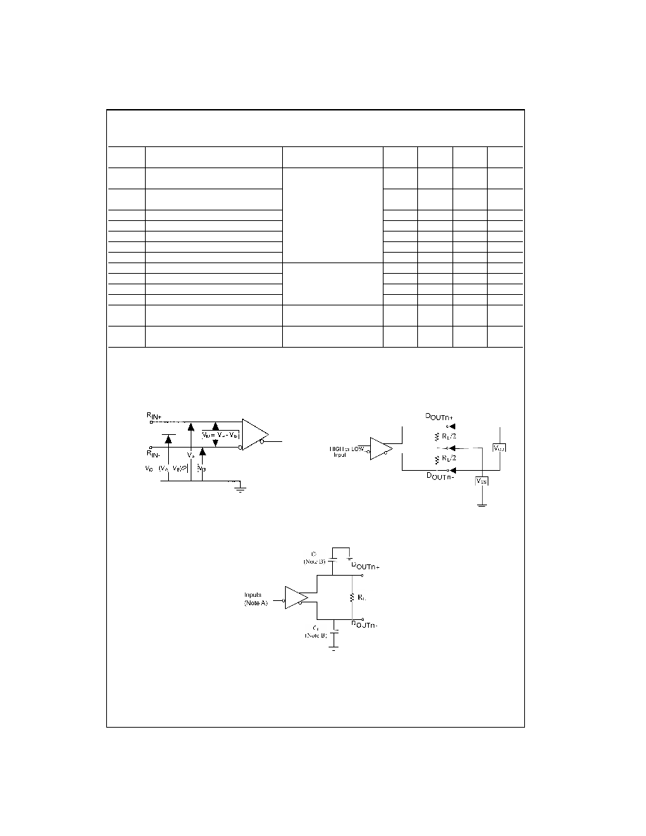
FIGURE 1. Differential Receiver Voltage Definitions and
Propagation I and Transition Time Test Circuit
FIGURE 2. Differential Driver DC Test Circuit
Note A: All LVDS input pulses have frequency
=
10MHz, t
R
or t
F
<
=
0.5 ns
Note B: C
L
includes all probe and test fixture capacitances
FIGURE 3. Differential Driver Propagation Delay and Transition Time Test Circuit
Symbol
Parameter
Test Conditions
Min
Typ
Max
Units
(Note 3)
t
PLHD
Differential Propagation Delay
0.75
1.1
1.75
ns
LOW-to-HIGH
t
PHLD
Differential Propagation Delay
R
L
=
100
, C
L
=
5 pF,
0.75
1.1
1.75
ns
HIGH-to-LOW
V
ID
=
200 mV to 450 mV,
t
TLHD
Differential Output Rise Time (20% to 80%)
V
IC
=
|V
ID
|/2 to (V
CC
-
(V
ID
/2),
0.29
0.40
0.58
ns
t
THLD
Differential Output Fall Time (80% to 20%)
Duty Cycle
=
50%,
0.29
0.40
0.58
ns
t
SK(P)
Pulse Skew |t
PLH
- t
PHL
|
See Figure 3 and Figure 4
0.01
0.2
ns
t
SK(PP)
Part-to-Part Skew (Note 4)
0.5
ns
f
MAX
Maximum Frequency (Note 5)(Note 6)
400
800
MHz
t
PZHD
Differential Output Enable Time from Z to HIGH
2.1
5
ns
t
PZLD
Differential Output Enable Time from Z to LOW
R
L
=
100
, C
L
=
5 pF,
2.3
5
ns
t
PHZD
Differential Output Disable Time from HIGH to Z See Figure 2 and Figure 3
1.5
5
ns
t
PLZD
Differential Output Disable Time from LOW to Z
1.8
5
ns
t
DJ
LVDS Data Jitter,
V
ID
=
300 mV, PRBS
=
2
23
-
1,
85
135
ps
Deterministic
V
IC
=
1.2V at 800 Mbps
t
RJ
LVDS Clock Jitter, Random
V
ID
=
300 mV
2.1
3.5
ps
(RMS)
V
IC
=
1.2 V at 400 MHz
www.fairchildsemi.com
4
FIN1
101
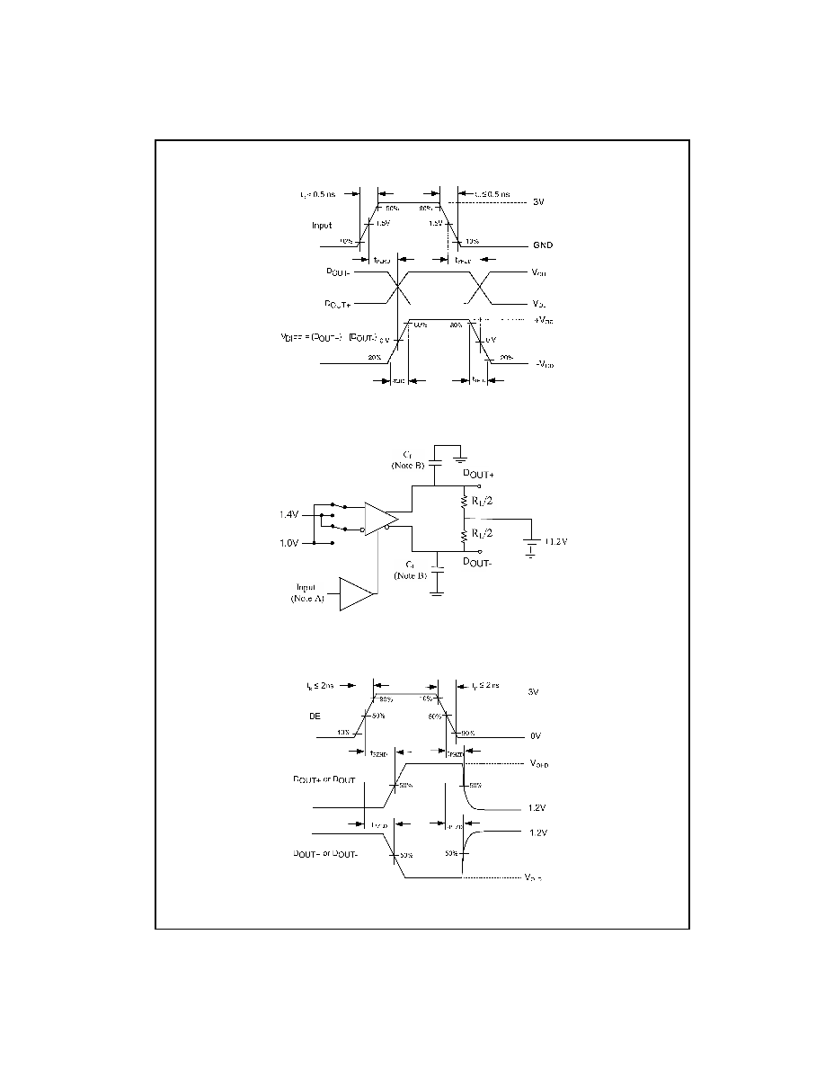
FIGURE 4. AC Waveforms
Note A: All LVTTL input pulses have frequency
=
10 MHz, t
R
or t
F
<
=
2 ns
Note B: C
L
includes all probe and test fixture capacitances
FIGURE 5. Differential Driver Enable and Disable Test Circuit
FIGURE 6. Enable and Disable AC Waveforms
5
www.fairchildsemi.com
FI
N1
101
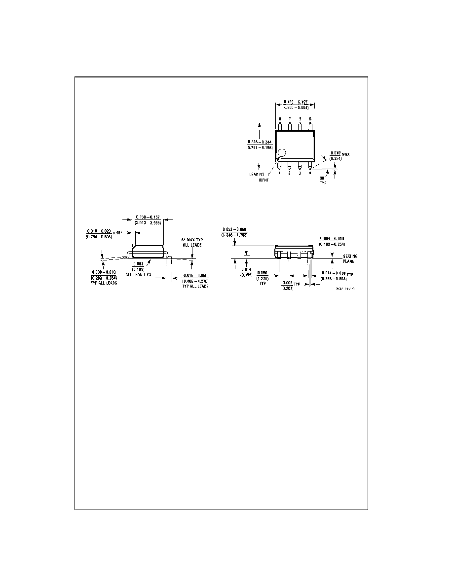
Physical Dimensions
inches (millimeters) unless otherwise noted
8-Lead Small Outline Integrated Circuit (SOIC), JEDEC MS-012, 0.150" Narrow
Package Number M08A