 | –≠–ª–µ–∫—Ç—Ä–æ–Ω–Ω—ã–π –∫–æ–º–ø–æ–Ω–µ–Ω—Ç: FIN1102 | –°–∫–∞—á–∞—Ç—å:  PDF PDF  ZIP ZIP |

© 2002 Fairchild Semiconductor Corporation
DS500657
www.fairchildsemi.com
January 2002
Revised February 2002
FI
N1
102 L
V
DS
2 Port
Hi
gh
Speed Repeat
er
FIN1102
LVDS 2 Port High Speed Repeater
General Description
This 2 port repeater is designed for high speed intercon-
nects utilizing Low Voltage Differential Signaling (LVDS)
technology. The FIN1102 accepts and outputs LVDS levels
with a typical differential output swing of 330 mV which pro-
vides low EMI at ultra low power dissipation even at high
frequencies. The FIN1102 provides a V
BB
reference for AC
coupling on the inputs. In addition the FIN1102 can also
directly accept LVPECL, HSTL, and SSTL-2 for translation
to LVDS.
Features
s
Greater than 800 Mbps full differential path
s
3.3V power supply operation
s
3.5 ps maximum random jitter and 135 ps maximum
deterministic jitter
s
Wide rail-to-rail common mode range
s
LVDS receiver inputs accept LVPECL, HSTL, and
SSTL-2 directly
s
Ultra low power consumption
s
20 ps typical channel-to-channel skew
s
Power off protection
s
>
7 kV HBM ESD Protection
s
Meets or exceeds the TIA/EIA-644-A LVDS standard
s
14-lead TSSOP package saves space
s
Open circuit fail safe protection
s
V
BB
reference output
Ordering Code:
Devices also available in Tape and Reel. Specify by appending suffix letter "X" to the ordering code.
Pin Descriptions
Function Table
H
=
HIGH Logic Level
L
=
LOW Logic Level
X
=
Don't Care
Z
=
High Impedance
Connection Diagram
Functional Diagram
Order Number
Package Number
Package Description
FIN1102MTC
MTC14
14-Lead Thin Shrink Small Outline Package (TSSOP), JEDEC MO-153, 4.4mm Wide
Pin Name
Description
R
IN1
+
, R
IN2
+
Non-inverting LVDS Input
R
IN1
-
, R
IN2
-
Inverting LVDS Input
D
OUT1
+
, D
OUT2
+
Non-inverting Driver Output
D
OUT1
-
, D
OUT2
-
Inverting Driver Output
EN
Driver Enable Pin for All Output
V
CC
Power Supply
GND
Ground
V
BB
Reference Voltage Output
Inputs
Outputs
EN
D
IN
+
D
IN
-
D
OUT
+
D
OUT
-
H
H
L
H
L
H
L
H
L
H
H
Fail Safe Case
H
L
L
X
X
Z
Z

www.fairchildsemi.com
2
FIN1
102
Absolute Maximum Ratings
(Note 1)
Recommended Operating
Conditions
Note 1: The "Absolute Maximum Ratings": are those values beyond which
damage to the device may occur. The databook specifications should be
met, without exception, to ensure that the system design is reliable over its
power supply, temperature and output/input loading variables. Fairchild
does not recommend operation of circuits outside databook specification.
DC Electrical Characteristics
Note 2: All typical values are at T
A
=
25
∞
C and with V
CC
=
3.3V.
Supply Voltage (V
CC
)
-
0.5V to
+
4.6V
LVDS DC Input Voltage (V
IN
)
-
0.5V to
+
4.6V
LVDS DC Output Voltage (V
OUT
)
-
0.5V to
+
4.6V
Driver Short Circuit Current (I
OSD
)
Continuous 10 mA
Storage Temperature Range (T
STG
)
-
65
∞
C to
+
150
∞
C
Max Junction Temperature (T
J
)
150
∞
C
Lead Temperature (T
L
)
(Soldering, 10 seconds)
260
∞
C
ESD (Human Body Model)
7000V
ESD (Machine Model)
300V
Supply Voltage (V
CC
)
3.0V to 3.6V
Magnitude of Differential
Voltage
(|V
ID
|)
100 mV to V
CC
Common Mode Voltage
Range (V
IC
)
(0V
+
|V
ID
|/2) to (V
CC
-
|V
ID
|/2)
Operating Temperature (T
A
)
-
40
∞
C to
+
85
∞
C
Symbol
Parameter
Test Conditions
Min
Typ
Max
Units
(Note 2)
V
TH
Differential Input Threshold HIGH See Figure 1; V
IC
=
+
0.05V,
+
1.2V, or V
CC
-
0.05V
100
mV
V
TL
Differential Input Threshold LOW
See Figure 1; V
IC
=
+
0.05V,
+
1.2V, or V
CC
-
0.05V
-
100
mV
V
IH
Input HIGH Voltage (EN)
2.0
V
CC
V
V
IL
Input LOW Voltage (EN)
GND
0.8
V
V
OD
Output Differential Voltage
250
330
450
mV
V
OD
V
OD
Magnitude Change from
25
mV
Differential LOW-to-HIGH
R
L
=
100
, Driver Enabled,
V
OS
Offset Voltage
See Figure 2
1.125
1.23
1.375
V
V
OS
Offset Magnitude Change from
25
mV
Differential LOW-to-HIGH
I
OS
Short Circuit Output Current
D
OUT
+
=
0V and D
OUT
-
=
0V,
-
3.4
-
6
mA
Driver Enabled
V
OD
=
0V, Driver Enabled
±
3.4
±
6
mA
I
IN
Input Current (EN, D
INx
+
, D
INx
-
)
V
IN
=
0V to V
CC
, Other Input
=
V
CC
or 0V
±
20
µ
A
(for Differential Inputs)
I
OFF
Power Off Input or Output Current V
CC
=
0V, V
IN
or V
OUT
=
0V to 3.6V
±
20
µ
A
I
CCZ
Disabled Power Supply Current
Drivers Disabled
4
7
mA
I
CC
Power Supply Current
Drivers Enabled, Any Valid Input Condition
16.7
23
mA
I
OZ
Disabled Output Leakage Current Driver Disabled, D
OUT
+
=
0V to 3.6V or
±
20
µ
A
D
OUT
-
=
0V to 3.6V
V
IC
Common Mode Voltage Range
|V
ID
|
=
100 mV to V
CC
0V
+
|V
ID
|/2
V
CC
-
(|V
ID
|/2)
V
C
IN
Input Capacitance
Enable Input
2.5
pF
LVDS Input
2.1
C
OUT
Output Capacitance
2.8
pF
V
BB
Output Reference Voltage
V
CC
=
3.3V, I
BB
=
0 to
-
275
µ
A
1.125
1.2
1.375
V
3
www.fairchildsemi.com
FI
N1
102
AC Electrical Characteristics
Over supply voltage and operating temperature ranges, unless otherwise specified
Note 3: All typical values are at T
A
=
25
∞
C and with V
CC
=
3.3V, V
ID
=
300 mV, V
IC
=
1.2V, unless otherwise specified.
Note 4: t
SK(LH)
, t
SK(HL)
is the skew between specified outputs of a single device when the outputs have identical loads and are switching in the same direc-
tion.
Note 5: t
SK(PP)
is the magnitude of the difference in differential propagation delay times between identical channels of two devices switching in the same
direction (either Low-to-HIGH or HIGH-to-LOW) when both devices operate with the same supply voltage, same temperature, and have identical test circuits.
Note 6: Passing criteria for maximum frequency is the output V
OD
>
200 mV and the duty cycle is 45% to 55% with all channels switching.
Note 7: Output loading is transmission line environment only; C
L
is
<
1 pF of stray test fixture capacitance.
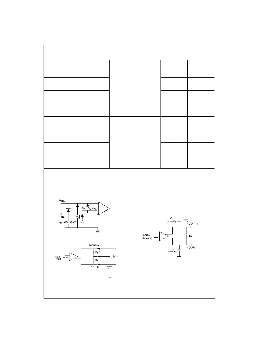
FIGURE 1. Differential Receiver Voltage Definitions and
Propagation and Transition Time Test Circuit
FIGURE 2. Differential Driver DC Test Circuit
Note A: All LVDS input pulses have frequency
=
10 MHz, t
R
or
t
F
<
=
0.5 ns
Note B: C
L
includes all probe and test fixture capacitances
FIGURE 3. Differential Driver Propagation Delay
and Transition Time Test Circuit
Symbol
Parameter
Test Conditions
Min
Typ
Max
Units
(Note 3)
t
PLHD
Differential Output Propagation Delay
0.75
1.1
1.75
ns
LOW-to-HIGH
t
PHLD
Differential Output Propagation Delay
0.75
1.1
1.75
ns
HIGH-to-LOW
R
L
=
100
, C
L
=
5 pF,
t
TLHD
Differential Output Rise Time (20% to 80%) |V
ID
|
=
200 mV to 450 mV,
0.29
0.4
0.58
ns
t
THLD
Differential Output Fall Time (80% to 20%)
V
IC
=
|V
ID
|/2 to V
CC
-
(|V
ID
|/2),
0.29
0.4
0.58
ns
t
SK(P)
Pulse Skew |t
PLH
- t
PHL
|
Duty Cycle
=
50%,
0.02
0.2
ns
t
SK(LH)
,
Channel-to-Channel Skew
See Figure 3 and Figure 4
0.02
0.15
ns
t
SK(HL)
(Note 4)
0.02
t
SK(PP)
Part-to-Part Skew (Note 5)
0.5
ns
f
MAX
Maximum Frequency (Note 6)(Note 7)
400
800
MHz
t
PZHD
Differential Output Enable Time
2.3
5
ns
from Z to HIGH
t
PZLD
Differential Output Enable Time
2.5
5
ns
from Z to LOW
R
L
=
100
, C
L
=
5 pF,
t
PHZD
Differential Output Disable Time
See Figure 5 and Figure 6
1.6
5
ns
from HIGH to Z
t
PLZD
Differential Output Disable Time
1.9
5
ns
from LOW to Z
t
DJ
LVDS Data Jitter,
|V
ID
|
=
300 mV, PRBS
=
2
23
- 1,
85
135
ps
Deterministic
V
IC
=
1.2V at 800 Mbps
t
RJ
LVDS Clock Jitter,
|V
ID
|
=
300 mV,
2.1
3.5
ps
Random (RMS)
V
IC
=
1.2V at 400 MHz

www.fairchildsemi.com
4
FIN1
102
FIGURE 4. AC Waveform
Note A: All input pulses have frequency
=
10MHz, t
R
or t
F
<
=
2 ns
Note B: C
L
includes all probe and test fixture capacitances
FIGURE 5. Differential Driver Enable and Disable Circuit
FIGURE 6. Enable and Disable AC Waveforms

5
www.fairchildsemi.com
FI
N1
102 L
V
DS
2 Port
Hi
gh
Speed Repeat
er
14-Lead Thin Shrink Small Outline Package (TSSOP), JEDEC MO-153, 4.4mm Wide
Package Number MTC14
Fairchild does not assume any responsibility for use of any circuitry described, no circuit patent licenses are implied and
Fairchild reserves the right at any time without notice to change said circuitry and specifications.
LIFE SUPPORT POLICY
FAIRCHILD'S PRODUCTS ARE NOT AUTHORIZED FOR USE AS CRITICAL COMPONENTS IN LIFE SUPPORT
DEVICES OR SYSTEMS WITHOUT THE EXPRESS WRITTEN APPROVAL OF THE PRESIDENT OF FAIRCHILD
SEMICONDUCTOR CORPORATION. As used herein:
1. Life support devices or systems are devices or systems
which, (a) are intended for surgical implant into the
body, or (b) support or sustain life, and (c) whose failure
to perform when properly used in accordance with
instructions for use provided in the labeling, can be rea-
sonably expected to result in a significant injury to the
user.
2. A critical component in any component of a life support
device or system whose failure to perform can be rea-
sonably expected to cause the failure of the life support
device or system, or to affect its safety or effectiveness.
www.fairchildsemi.com