 | ÐлекÑÑоннÑй компоненÑ: FIN12AC | СкаÑаÑÑ:  PDF PDF  ZIP ZIP |
Äîêóìåíòàöèÿ è îïèñàíèÿ www.docs.chipfind.ru
Preliminary
© 2005 Fairchild Semiconductor Corporation
DS500915
www.fairchildsemi.com
April 2005
Revised May 2005
FI
N12AC
P
SerDes
¥
FIN12AC
P
SerDes
¥
Low Voltage 12-Bit Bi-Directional Serializer/Deserializer
with Multiple Frequency Ranges (Preliminary)
General Description
The FIN12AC is a 12-bit serializer capable of running a
parallel frequency range between 5MHz and 56MHz. The
frequency range is selected by the S1 and S2 control sig-
nals. The bi-directional data flow is controlled through use
of a direction (DIRI) control pin. The devices can be config-
ured to operate in a unidirectional mode only by hardwiring
the DIRI pin. An internal PLL generates the required bit
clock frequency for transfer across the serial link. Options
exist for dual or single PLL operation dependent upon sys-
tem operational parameters. The device has been
designed for low power operation and utilizes Fairchild Pro-
prietary Low Power CTL interface. The device also sup-
ports an ultra low power Power-Down mode for conserving
power in battery operated applications.
Features
s
Low power consumption
s
Fairchild Proprietary Low Power CTL interface
s
LVCMOS parallel I/O interface
· 2 mA source/sink current
· Over-voltage tolerant control signals
s
I/O power supply range between 1.65V and 3.6V
s
Analog Power Supply range of 2.775V
r
5%
s
Multi-Mode operation allows for a single device to
operate as Serializer or Deserializer
s
Internal PLL with no external components
s
Standby Power-Down mode support
s
Small footprint 32-terminal MLP packaging
s
Built in differential termination
s
Supports external CKREF frequencies between
5MHz and 56MHz
s
Serialized data rate up to 784Mb/s
Ordering Code:
Pb-Free package per JEDEC J-STD-020B.
BGA and MLP packages available in Tape and Reel only.
P
SerDes
¥
is a trademark of Fairchild Semiconductor Corporation.
Order Number
Package Number
Package Description
FIN12ACGFX
(Preliminary)
BGA42A
Pb-Free 42-Ball Ultra Small Scale Ball Grid Array (USS-BGA), JEDEC MO-195,
3.5mm Wide
FIN12ACMLX
MLP032A
Pb-Free 32-Terminal Molded Leadless Package (MLP), Quad, JEDEC MO-220, 5mm
Square
Preliminary
www.fairchildsemi.com
2
FI
N12AC
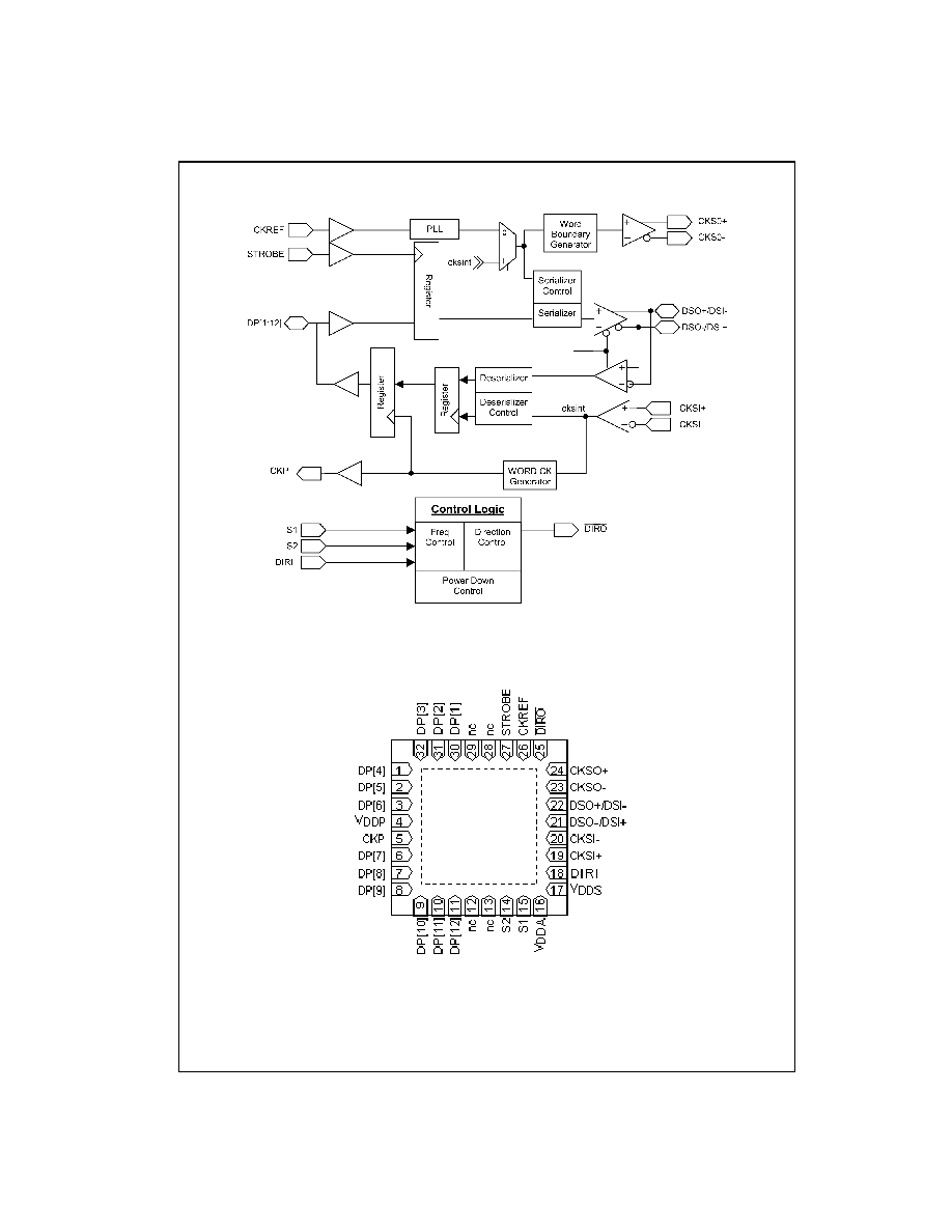
Functional Block Diagram
Connection Diagram
Terminal Assignments for MLP
(Top View)
Preliminary
3
www.fairchildsemi.com
FI
N12AC
Pin Description
Note 1: The DSO/DSI serial port terminals have been arranged such that when one device is rotated 180 degrees with respect to the other device the serial
connections will properly align without the need for any traces or cable signals to cross. Other layout orientations may require that traces or cables cross.
Control Logic Circuitry
The FIN12AC has the ability to be used as a 12-bit Serial-
izer or a 12-bit Deserializer. Terminals S1 and S2 must be
set to accommodate the clock reference input frequency
range of the serializer. The table below shows the terminal
programming of these options based on the S1 and S2
control terminals. The DIRI terminal controls whether the
device is the serializer or a deserializer. When DIRI is
asserted LOW, the device is configured as a deserializer.
When the DIRI terminal is asserted HIGH, the device will
be configured as a serializer. Changing the state on the
DIRI signal will reverse the direction of the I/O signals and
generate the opposite state signal on DIRO. For unidirec-
tional operation the DIRI terminal should be hardwired to
the HIGH or LOW state and the DIRO terminal should be
left floating. For bi-directional operation the DIRI of the
master device will be driven by the system and the DIRO
signal of the master will be used to drive the DIRI of the
slave device.
Turn-Around Functionality
The device passes and inverts the DIRI signal through the
device asynchronously to the DIRO signal. Care must be
taken by the system designer to insure that no contention
occurs between the deserializer outputs and the other
devices on this port. Optimally the peripheral device driving
the serializer should be put into a HIGH Impedance state
prior to the DIRI signal being asserted.
When a device with dedicated data outputs turns from a
deserializer to a serializer the dedicated outputs will remain
at the last logical value asserted. This value will only
change if the device is once again turned around into a
deserializer and the values are overwritten.
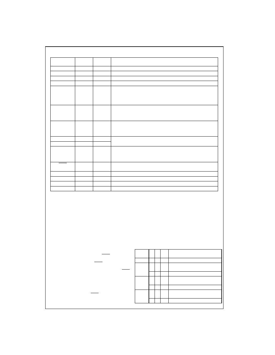
TABLE 1. Control Logic Circuitry
Pin Name
I/O Type
Number
of Pins
Description of Signals
DP[1:12]
I/O
12
LVCMOS Parallel I/O. Direction controlled by DIRI terminal.
CKREF
IN
1
LVCMOS Clock Input and PLL Reference
STROBE
IN
1
LVCMOS Strobe Signal for Latching Data into the Serializer
CKP
OUT
1
LVCMOS Word Clock Output
DSO
/ DSI
DSO
/ DSI
DIFF-I/O
2
CTL Differential Serial I/O Data Signals (Note )
DSO: Refers to output signal pair
DSI: Refers to input signal pair
DSO(I)
: Positive signal of DSO(I) pair
DSO(I)
: Negative signal of DSO(I) pair
CKSI
, SKSI
DIFF-IN
2
CTL Differential Deserializer Input Bit Clock
CKSI: Refers to signal pair
CKSI
: Positive signal of CKSI pair
CKSI
: Negative signal of CKSI pair
CKSO
, CKSO
DIFF-OUT
2
CTL Differential Serializer Output Bit Clock
CKSO: Refers to signal pair
CKSO
: Positive signal of CKSO pair
CKSO
: Negative signal of CKSO pair
S1
IN
1
LVCMOS Mode Selection terminals used to define
S2
IN
1
frequency range for the RefClock, CKREF
DIRI
IN
1
LVCMOS Control Input
Used to control direction of Data Flow:
DIRI
"1" Serializer,
DIRI
"0" Deserializer
DIRO
OUT
1
LVCMOS Control Output
Inversion of DIRI
V
DDP
Supply
1
Power Supply for Parallel I/O and Translation Circuitry
V
DDS
Supply
1
Power Supply for Core and Serial I/O
V
DDA
Supply
1
Power Supply for Analog PPL Circuitry
GND
Supply
0
Use Bottom Ground Plane for Ground Signals
Mode
Number
S2 S1 DIRI
Description
0
0
0
X
Power-Down Mode
1
0
1
1
12-Bit Serializer,
20MHz to 56MHz CKREF
0
1
0
12-Bit Deserializer
2
1
0
1
12-Bit Serializer,
5MHz to 15MHz CKREF
1
0
0
12-Bit Deserializer
3
1
1
1
12-Bit Serializer,
10MHz to 30MHz CKREF
1
1
0
12-Bit Deserializer

Preliminary
www.fairchildsemi.com
4
FI
N12AC
Power-Down Mode
Mode 0 is used for powering down and resetting the
device. When both of the mode signals are driven to a
LOW state the PLL and references will be disabled, differ-
ential input buffers will be shut off, differential output buffers
will be placed into a HIGH Impedance state, LVCMOS out-
puts will be placed into a HIGH Impedance state, and LVC-
MOS inputs will be driven to a valid level internally.
Additionally all internal circuitry will be reset. The loss of
CKREF state is also enabled to insure that the PLL will only
power-up if there is a valid CKREF signal.
In a typical application mode signals of the device will not
change other than between the desired frequency range
and the power-down mode. This allows for system level
power-down functionality to be implemented via a single
wire for a SerDes pair. The S1 and S2 selection signals
that have their operating mode driven to a "logic 0" should
be hardwired to GND. The S1 and S2 signals that have
their operating mode driven to a "logic 1" should be con-
nected to a system level power-down signal.
Serializer Operation Mode
The serializer configurations are described in the following
sections. The basic serialization circuitry works essentially
identical in these modes but the actual data and clock
streams will differ dependent on if CKREF is the same as
the STROBE signal or not. When it is stated that CKREF
STROBE this means that the CKREF and STROBE signals
have an identical frequency of operation but may or may
not be phase aligned. When it is stated that CKREF does
not equal STROBE then each signal is distinct and CKREF
must be running at a frequency high enough to avoid any
loss of data condition. CKREF must never be a lower fre-
quency than STROBE.
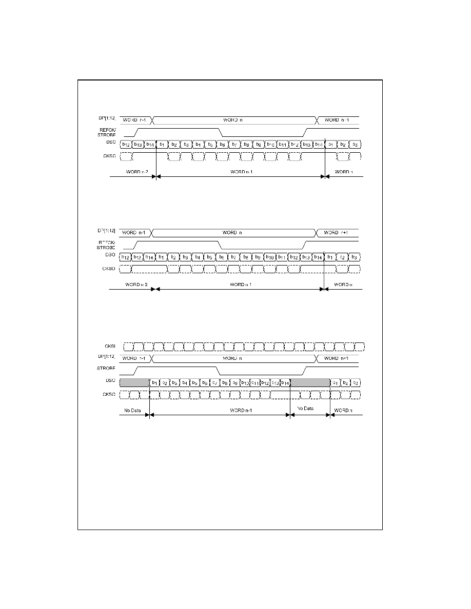
Serializer Operation: (Figure )
Modes 1, 2, or 3
DIRI equals 1
CKREF equals STROBE
The PLL must receive a stable CKREF signal in order to
achieve lock prior to any valid data being sent. The CKREF
signal can be used as the data STROBE signal provided
that data can be ignored during the PLL lock phase.
Once the PLL is stable and locked the device can begin to
capture and serialize data. Data will be captured on the ris-
ing edge of the STROBE signal and then serialized. The
serialized data stream is synchronized and sent source
synchronously with a bit clock with an embedded word
boundary. When operating in this mode the internal deseri-
alizer circuitry is disabled including the DS input buffer. The
CKSI serial inputs remain active to allow the pass through
of the CKSI signal to the CKP output. For more on this
mode please see the section on Passing a Word Clock. If
this mode is not needed then the CKSI inputs can either be
driven to valid levels or left to float. For lowest power oper-
ation let the CKSI inputs float.
Serializer Operation: (Figure )
DIRI equals 1
CKREF does not equal STOBE
If the same signal is not used for CKREF and STROBE,
then the CKREF signal must be run at a higher frequency
than the STROBE rate in order to serialize the data cor-
rectly. The actual serial transfer rate will remain at 14 times
the CKREF frequency. A data value of zero will be sent
when no valid data is present in the serial bit stream. The
operation of the serializer will otherwise remain the same.
The exact frequency that the reference clock needs to run
at will be dependent upon the stability of the CKREF and
STROBE signal. If the source of the CKREF signal imple-
ments spread spectrum technology then the minimum fre-
quency of this spread spectrum clock should be used in
calculating the ratio of STROBE frequency to the CKREF
frequency. Similarly if the STROBE signal has significant
cycle-to-cycle variation then the maximum cycle-to-cycle
time needs to be factored into the selection of the CKREF
frequency.
Serializer Operation: (Figure )
DIRI equals 1
No CKREF
A third method of serialization can be done by providing a
free running bit clock on the CKSI signal. This mode is
enabled by grounding the CKREF signal and driving the
DIRI signal HIGH.
At power-up the device is configured to accept a serializa-
tion clock from CKSI. If a CKREF is received then this
device will enable the CKREF serialization mode. The
device will remain in this mode even if CKREF is stopped.
To re-enable this mode the device must be powered down
and then powered back up with "logic 0" on CKREF.
Preliminary
5
www.fairchildsemi.com
FI
N12AC
Serializer Operation Mode
(Continued)
FIGURE 1. Serializer Timing Diagram (CKREF equals STROBE)
FIGURE 2. Serializer Timing Diagram (CKREF does not equal STROBE)
FIGURE 3. Serializer Timing Diagram Using Provided Bit Clock (No CKREF)