 | –≠–ª–µ–∫—Ç—Ä–æ–Ω–Ω—ã–π –∫–æ–º–ø–æ–Ω–µ–Ω—Ç: FIN24C | –°–∫–∞—á–∞—Ç—å:  PDF PDF  ZIP ZIP |
© 2005 Fairchild Semiconductor Corporation
DS500909
www.fairchildsemi.com
April 2005
Revised September 2005
FIN24C
P
Se
r
D
es
•
Low V
o
lt
a
g
e 2
4
-Bit Bi-Direc
ti
onal S
e
ria
lize
r
/Des
eri
a
lize
r
FIN24C
P
SerDes
•
Low Voltage 24-Bit Bi-Directional Serializer/Deserializer
General Description
The FIN24C
P
SerDes
•
is a low power Serializer/Deserializer
(SerDes) that can help minimize the cost and power of transfer-
ring wide signal paths. Through the use of serialization, the
number of signals transferred from one point to another can be
significantly reduced. Typical reduction is 4:1 to 6:1 for unidirec-
tional paths. For bi-directional operation, using half duplex for
multiple sources, it is possible to increase the signal reduction
to close to 10:1. Through the use of differential signaling, shield-
ing and EMI filters can also be minimized, further reducing the
cost of serialization. The differential signaling is also important
for providing a noise-insensitive signal that can withstand radio
and electrical noise sources. Major reduction in power con-
sumption allows minimal impact on battery life in ultra-portable
applications. A unique word boundary technique assures that
the actual word boundary is identified when the data is deserial-
ized. This guarantees that each word is correctly aligned at the
deserializer on a word by word basis through a unique
sequence of clock and data that is not repeated except at the
word boundary. It is possible to use a single PLL for most appli-
cations including bi-directional operation.
Features
O
Low power for minimum impact on battery life
∑ Multiple power-down modes
∑ AC coupling with DC balance
O
100nA in standby mode
5mA typical operating conditions
O
Cable reduction:
25:4 or greater
O
Bi-directional operation 50:7 reduction or greater
O
Up to 24 bits in either direction
O
Up to 20MHz parallel interface operation
O
Voltage translation from 1.8V to 3.3V
O
Ultra-small and cost-effective packaging
O
High ESD protection:
!
8kV HBM
Applications
O
Micro-controller or Pixel interfaces
O
Image sensors
O
Small displays
LCD, cell phone, digital camera, portable gaming, printer,
PDA, video camera, automotive
Ordering Code:
Pb-Free package per JEDEC J-STD-020B.
BGA and MLP packages available in Tape and Reel only.
P
SerDes
•
is a trademark of Fairchild Semiconductor Corporation.
Order
Number
Package
Number
Package Description
FIN24CGFX
(Preliminary)
BGA042A
Pb-Free 42-Ball Ultra Small Scale Ball Grid Array (USS-BGA), JEDEC MO-195, 3.5mm Wide
FIN24CMLX
MLP040A
Pb-Free 40-Terminal Molded Leadless Package (MLP), Quad, JEDEC MO-220, 6mm Square
www.fairchildsemi.com
2
FIN24C
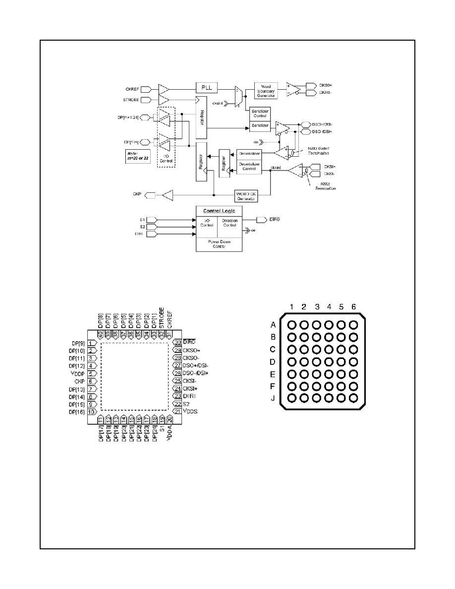
Functional Block Diagram
Connection Diagrams
Terminal Assignments for MLP
(Top View)
Terminal Assignments for
P
BGA
(Top View)
3
www.fairchildsemi.com
FIN24C
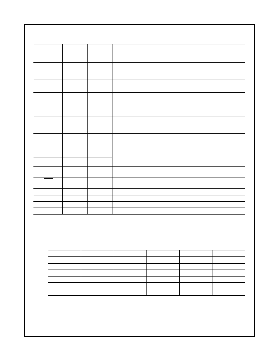
MLP Terminal Description
Note 1: The DSO/DSI serial port terminals have been arranged such that when one device is rotated 180 degrees with the other device the serial connections will properly align
without the need for any traces or cable signals to cross. Other layout orientations may require that traces or cables cross.
P
BGA Terminal Assignments
MLP
Terminal
Name
I/O Type
Number of
Terminals
Description of Signals
DP[1:20]
I/O
20
LVCMOS Parallel I/O. Direction controlled by DIRI Terminal
DP[21:24]
I or O
4
LVCMOS Parallel Unidirectional Inputs or Outputs Dependent on State of S1, S2
Terminals
CKREF
IN
1
LVCMOS Clock Input and PLL Reference
STROBE
IN
1
LVCMOS Strobe Signal for Latching Data into the Serializer
CKP
OUT
1
LVCMOS Word Clock Output
DSO
/ DSI
DSO
/ DSI
DIFF-I/O
2
CTL Differential Serial I/O Data Signals (Note 1)
DSO: Refers to output signal pair
DSI: Refers to input signal pair
DSO(I)
: Positive signal of DSO(I) pair
DSO(I)
: Negative signal of DSO(I) pair
CKSI
, CKSI
DIFF-IN
2
CTL Differential Deserializer Input Bit Clock
CKSI: Refers to signal pair
CKSI
: Positive signal of CKSI pair
CKSI
: Negative signal of CKSI pair
CKSO
, CKSO
DIFF-OUT
2
CTL Differential Serializer Output Bit Clock
CKSO: Refers to signal pair
CKSO
: Positive signal of CKSO pair
CKSO
: Negative signal of CKSO pair
S1
IN
1
LVCMOS Mode Selection Pins used to define mode of operation for some
terminals. The control terminals, DP[21:24] can be set as 4 terminals in the same
direction or two in each direction.
S2
IN
1
DIRI
IN
1
LVCMOS Control Input
Used to control direction of Data Flow
DIRO
OUT
1
LVCMOS Control Output
Inversion of DIRI
V
DDP
Supply
1
Power Supply for Parallel I/O and Translation Circuitry
V
DDS
Supply
1
Power supply for core circuitry and serial I/O
V
DDA
Supply
1
Power Supply for Analog PLL Circuitry
GND
Supply
0
Use Bottom Ground Plane for Ground Signals
1
2
3
4
5
6
A
DP[9]
DP[7]
DP[5]
DP[3]
DP[1]
CKREF
B
DP[11]
DP[10]
DP[6]
DP[2]
STROBE
DIRO
C
CKP
DP[12]
DP[8]
DP[4]
CKSO
CKSO
D
DP[13]
DP[14]
V
DDP
GND
DSO
/ DSI
DSO
/ DSI
E
DP[15]
DP[16]
GND
V
DDS
CKSI
CKSI
F
DP[17]
DP[18]
DP[21]
V
DDA
S2
DIRI
J
DP[19]
DP[20]
DP[22]
DP[23]
DP[24]
S1
www.fairchildsemi.com
4
FIN24C
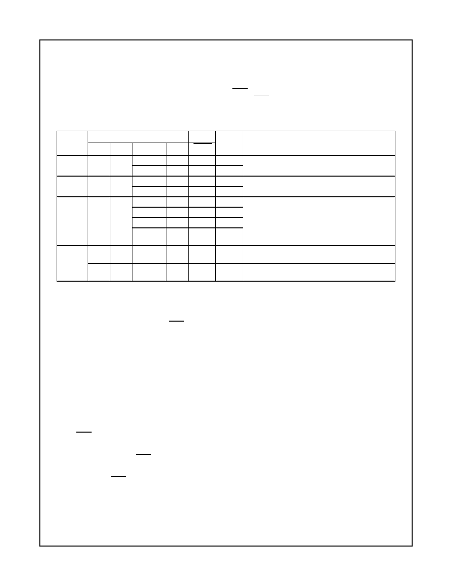
Control Logic Circuitry
The FIN24C has 4 signals that are selectable as 2 unidirectional
inputs and 2 unidirectional outputs, or as 4 unidirectional inputs
or 4 unidirectional outputs. These are often used by applications
for control signals. The mode signals S1 and S2 determine the
direction of the DP[21:24] data signals. The 00 state also pro-
vides for a power-down state where all functionality of the
device is disabled or reset. The DIRI terminal controls the direc-
tion of the device when operating in Modes 1 and 3. When in
Mode 2 the direction is controlled by both the DIRI and
STROBE signals. Table 1 provides a complete description of
the various modes of operation. For unidirectional operation the
DIRI terminal should be hardwired to a valid logic level and the
DIRO terminal should be left floating. For bi-directional opera-
tion the DIRO of the master device should be connected to the
DIRI of the slave device.
TABLE 1. Control Logic Circuitry
When operating in a bi-directional mode the turn around func-
tionality varies dependent upon the mode of the device. For
Modes 1 and 3 the device asynchronously passes and inverts
the DIRI signal through the device to the DIRO signal. Care
must be taken by the system designer to insure that no conten-
tion occurs between the deserializer outputs and the other
devices on this port. Optimally the peripheral device driving the
serializer should be put into a HIGH Impedance state prior to
the DIRI signal being asserted.
When a device with dedicated data outputs turns from a deseri-
alizer to a serializer the dedicated outputs will remain at the last
logical value asserted. This value will only change if the device
is once again turned around into a deserializer and the values
are overwritten.
When the device is in Mode 2 (S2 = 1, S1 = 0) the direction of
operation is dependent upon both the STROBE signal and the
DIRI signal. At power-up the mode select signals are both LOW
and the DIRO signal will be the inversion of the DIRI signal.
After power-up the DIRI and STROBE signal should initially
both be HIGH. When STROBE goes LOW the device will be
configured as a serializer and DIRO will be forced LOW. The
device will remain as a serializer until the DIRI signal goes
LOW. When DIRI goes LOW the device will be re-configured as
a deserializer and the DIRO signal will be asserted HIGH.
When operating the SerDes in pairs not all operating modes are
compatible. Regardless of the mode of operation the serializer
is always sending 24 bits of data and 2 word boundary bits. The
deserializer is always receiving 24 bits of data and 2 word
boundary bits. For some modes of operation not all of the data
bits are valid due to some pins being dedicated inputs or out-
puts. A value of "0" will be sent in the serial stream for all invalid
data bits.
4-Bit Control Mode: When operating in 4-bit control mode the
master device must be configured as MODE 2.
(S2 = 1, S1 = 0) and the slave device must be con-
figured as MODE 1 (S2 = 0, S1 = 1). When operat-
ing in this mode 24 data and control bits can be sent
from the master to the slave and 20 data bits can be
sent from the slave to the master. Unidirectional con-
trol signals should be connected to DP[21:24].
2-Bit Control Mode: When operating in 2-bit control mode
both devices must be configured in MODE 3
(S2 = S1 = "1"). In this mode of operation 22 bits can
be sent in either direction. When operating in a 2-bit
control mode serialized bits 21 and 22 will appear on
outputs 23 and 24 of the deserializer.
Mode
Inputs
Output Device
Description
Number
S2
S1
STROBE DIRI
DIRO
State
0
0
0
x
0
1
na
Power-Down State. The device will be powered
x
1
0
na
down and disabled regardless of all other signals
1
0
1
x
0
1
Des
4-Bit Unidirectional Control Mode. DP[21:24] are outputs.
x
1
0
Ser
2
1
0
0
0
1
Des
4-Bit Unidirectional Control Mode. DP[21:24] are inputs.
STROBE and DIRI operate as an RS-Latch to change the
state of operation.
In general DIRI and Strobe should not be LOW at the
same time.
0
1
0
Ser
1
0
1
Des
1
1
DIRO
(n-1)
Previous
3
1
1
x
0
1
Des
2-Bit Unidirectional Control Mode. DP[21:22] are Inputs.
DP[23:24] Outputs
1
1
x
1
0
Ser
2-Bit Unidirectional Control Mode. DP[21:22] are Inputs.
DP[23:24] Outputs

5
www.fairchildsemi.com
FIN24C
Power-Down Mode: (Mode 0)
Mode 0 is used for powering down and resetting the device.
When both of the mode signals are driven to a LOW state the
PLL and references will be disabled, differential input buffers will
be shut off, differential output buffers will be placed into a HIGH
Impedance state, LVCMOS outputs will be placed into a HIGH
Impedance state and LVCMOS inputs will be driven to a valid
level internally. Additionally all internal circuitry will be reset. The
loss of CKREF state is also enabled to insure that the PLL will
only power-up if there is a valid CKREF signal.
In a typical application the device will only change between the
power-down mode and the selected mode of operation. This
allows for system level power-down functionality to be imple-
mented via a single wire for a SerDes pair. The S1 and S2
selection signals that have their operating mode driven to a
"logic 0" should be hardwired to GND. The S1 and S2 signals
that have their operating mode driven to a "logic 1" should be
connected to a system level power-down signal.
Serializer Operation
The serializer configuration is described in the following sec-
tions. The basic serialization circuitry works essentially identi-
cally in these modes, but the actual data and clock streams will
differ depending on if CKREF is the same as the STROBE sig-
nal or not. When it is stated that CKREF equals STROBE this
means that the CKREF and STROBE signals are hardwired
together as one signal. When it is stated that CKREF does not
equal STROBE then each signal is distinct and CKREF must be
running at a frequency high enough to avoid any loss of data
condition. CKREF must never be a lower frequency than
STROBE.
Serializer Operation: (Figure 1)
DIRI equals 1
CKREF equals STROBE
The PLL must receive a stable CKREF signal in order to
achieve lock prior to any valid data being sent. The CKREF sig-
nal can be used as the data STROBE signal provided that data
can be ignored during the PLL lock phase.
Once the PLL is stable and locked the device can begin to cap-
ture and serialize data. Data will be captured on the rising edge
of the STROBE signal and then serialized. The serialized data
stream is synchronized and sent source synchronously with a
bit clock with an embedded word boundary. Serialized data is
sent at 26 times the CKREF clock rate. Two additional data bits
are sent that define the word boundary. When operating in this
mode the internal deserializer circuitry is disabled including the
serial clock, serial data input buffers, the bidirectional parallel
outputs and the CKP word clock. The CKP word clock will be
driven HIGH.
Serializer Operation: (Figure 2)
DIRI equals 1
CKREF does not equal STROBE
If the same signal is not used for CKREF and STROBE, then
the CKREF signal must be run at a higher frequency than the
STROBE rate in order to serialize the data correctly. The actual
serial transfer rate will remain at 26 times the CKREF fre-
quency. A data bit value of zero will be sent when no valid data
is present in the serial bit stream. The operation of the serializer
will otherwise remain the same.
The exact frequency that the reference clock needs to run at will
be dependent upon the stability of the CKREF and STROBE
signal. If the source of the CKREF signal implements spread
spectrum technology then the maximum frequency of this
spread spectrum clock should be used in calculating the ratio of
STROBE frequency to the CKREF frequency. Similarly if the
STROBE signal has significant cycle-to-cycle variation then the
maximum cycle-to-cycle time needs to be factored into the
selection of the CKREF frequency.
Serializer Operation: (Figure 3)
DIRI equals 1
No CKREF
A third method of serialization can be done by providing a free
running bit clock on the CKSI signal. This mode is enabled by
grounding the CKREF signal and driving the DIRI signal HIGH.
At power-up the device is configured to accept a serialization
clock from CKSI. If a CKREF is received then the device will
enable the CKREF serialization mode. The device will remain in
this mode even if CKREF is stopped. To re-enable this mode
the device must be powered down and then powered back up
with "logic 0" on CKREF.