Äîêóìåíòàöèÿ è îïèñàíèÿ www.docs.chipfind.ru
© 2004 Fairchild Semiconductor Corporation
DS500864
www.fairchildsemi.com
October 2003
Revised January 2004
FI
N3385 ·
FI
N3383 Low
V
o
l
t
age 28-
B
i
t
Fl
at Panel
Di
splay Li
nk
Ser
i
al
iz
ers
FIN3385 · FIN3383
Low Voltage 28-Bit Flat Panel Display Link Serializers
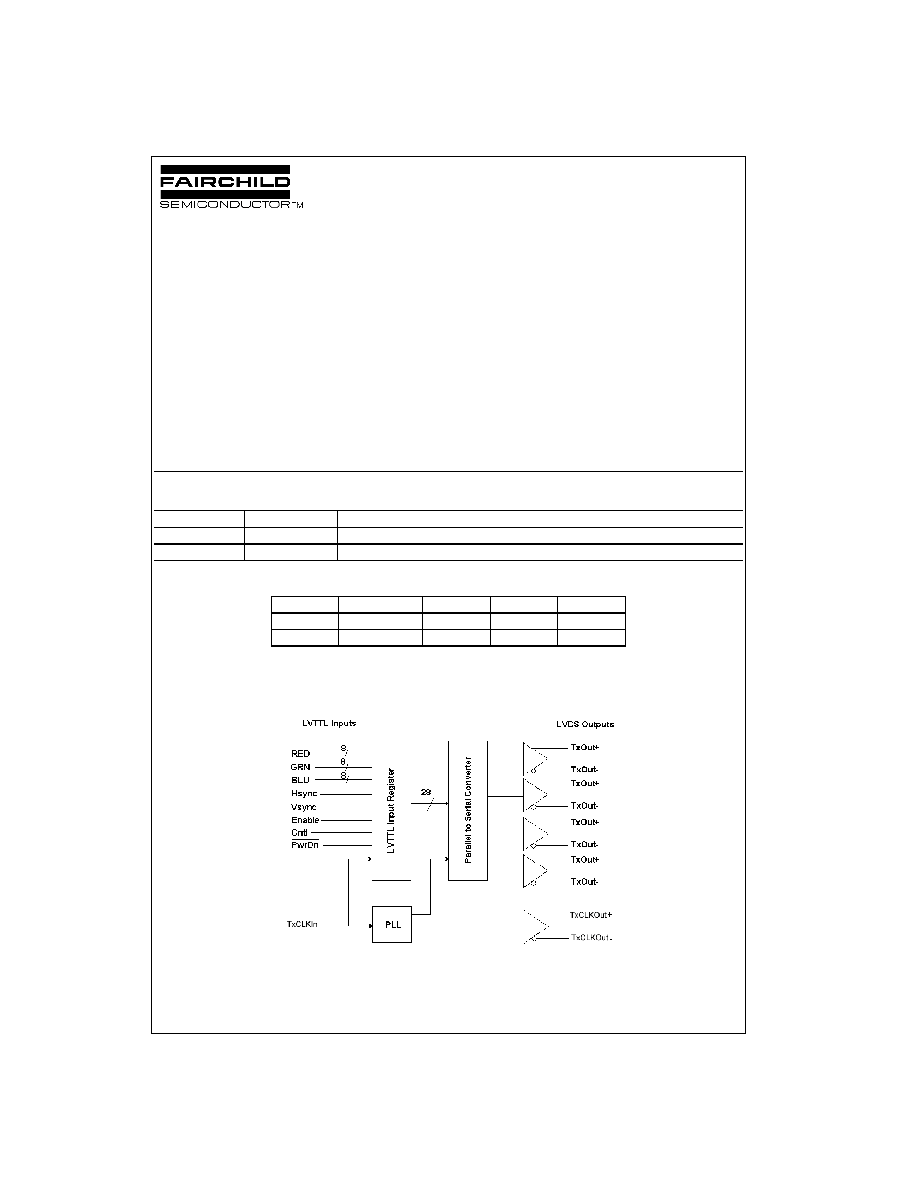
General Description
The FIN3385 and FIN3383 transform 28 bit wide parallel
LVTTL (Low Voltage TTL) data into 4 serial LVDS (Low
Voltage Differential Signaling) data streams. A phase-
locked transmit clock is transmitted in parallel with the data
steam over a separate LVDS link. Every cycle of transmit
clock 28 bits of input LVTTL data are sampled and trans-
mitted.
These chipsets are an ideal solution to solve EMI and
cable size problems associated with wide and high-speed
TTL interfaces.
Features
s
Low power consumption
s
20 MHz to 85 MHz shift clock support
s
±
1V common-mode range around 1.2V
s
Narrow bus reduces cable size and cost
s
High throughput (up to 2.38 Gbps throughput)
s
Internal PLL with no external component
s
Compatible with TIA/EIA-644 specification
s
Devices are offered in 48- and 56-lead TSSOP
packages
Ordering Code:
Devices also available in Tape and Reel. Specify by appending suffix letter "X" to the ordering code.
TABLE 1. Display Panel Link Serializers/De-Serializers Chip Matrix
Block Diagram
Functional Diagram for FIN3385 and FIN3383
Order Number
Package Number
Package Description
FIN3383MTD
MTD56
56-Lead Thin Shrink Small Outline Package (TSSOP), JEDEC MO-153, 6.1mm Wide
FIN3385MTD
MTD56
56-Lead Thin Shrink Small Outline Package (TSSOP), JEDEC MO-153, 6.1mm Wide
Part
CLK Frequency
LVTTL IN
LVDS OUT
Package
FIN3385
85
28
4
56 TSSOP
FIN3383
66
28
4
56 TSSOP
www.fairchildsemi.com
2
FIN338
5
·
FIN3383
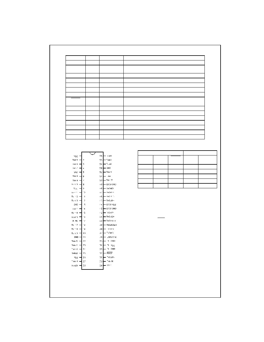
Pin Descriptions
Connection Diagram
Truth Table
H
=
HIGH Logic Level
L
=
LOW Logic Level
X
=
Don't Care
Z
=
High Impedance
F
=
Floating
Note 1: The outputs of the transmitter or receiver will remain in a
High Impedance state until V
CC
reaches 2V.
Note 2: TxCLKOut
±
will settle at a free running frequency when the
part is powered up, PwrDn is HIGH and the TxCLKIn is a steady logic
level (L/H/Z).
Pin Names
I/O Type Number of Pins
Description of Signals
TxIn
I
28/21
LVTTL Level Inputs
TxCLKIn
I
1
LVTTL Level Clock Input
The rising edge is for data strobe.
TxOut
+
O
4/3
Positive LVDS Differential Data Output
TxOut
-
O
4/3
Negative LVDS Differential Data Output
TxCLKOut
+
O
1
Positive LVDS Differential Clock Output
TxCLKOut
-
O
1
Negative LVDS Differential Clock Output
R_FB
I
1
Rising Edge Clock (HIGH), Falling Edge Clock (LOW)
PwrDn
I
1
LVTTL Level Power-Down Input
Assertion (LOW) puts the outputs in High Impedance state.
PLL V
CC
I
1
Power Supply Pin for PLL
PLL GND
I
2
Ground Pins for PLL
LVDS V
CC
I
1
Power Supply Pin for LVDS Outputs
LVDS GND
I
3
Ground Pins for LVDS Outputs
V
CC
I
3
Power Supply Pins for LVTTL Inputs
GND
I
5
Ground pins for LVTTL Inputs
NC
No Connect
Inputs
Outputs
TxIn
TxCLKIn
PwrDn
(Note 1)
TxOut
±
TxCLKOut
±
Active
Active
H
L/H
L/H
Active
L/H/Z
H
L/H
X (Note 2)
F
Active
H
L
L/H
F
F
H
L
X (Note 2)
X
X
L
Z
Z
3
www.fairchildsemi.com
FI
N3385
·
FI
N3383
Absolute Maximum Ratings
(Note 3)
Recommended Operating
Conditions
Note 3: Absolute maximum ratings are DC values beyond which the device
may be damaged or have its useful life impaired. The datasheet specifica-
tions should be met, without exception, to ensure that the system design is
reliable over its power supply, temperature, and output/input loading vari-
ables. Fairchild does not recommend operation outside datasheet specifi-
cations.
Note 4: 100mV V
CC
noise should be tested for frequency at least up to
2 MHz. All the specification below should be met under such a noise.
DC Electrical Characteristics
Over supply voltage and operating temperature ranges, unless otherwise specified. (Note 5)
Note 5: All Typical values are at T
A
=
25
°
C and with V
CC
=
3.3V.
Note 6: Positive current values refer to the current flowing into device and negative values means current flowing out of pins. Voltage are referenced to
ground unless otherwise specified (except
V
OD
and V
OD
).
Note 7: The power supply current for both transmitter and receiver can be different with the number of active I/O channels.
Note 8: The 16-grayscale test pattern tests device power consumption for a "typical" LCD display pattern. The test pattern approximates signal switching
needed to produce groups of 16 vertical strips across the display.
Power Supply Voltage (V
CC
)
-0.3V to +4.6V
TTL/CMOS Input/Output Voltage
-
0.5V to
+
4.6V
LVDS Input/Output Voltage
-0.3V to +4.6V
LVDS Output Short Circuit Current (I
OSD
)
Continuous
Storage Temperature Range (T
STG
)
-
65
°
C to
+
150
°
C
Maximum Junction Temperature (T
J
)
150
°
C
Lead Temperature (T
L
)
(Soldering, 4 seconds)
260
°
C
ESD Rating (HBM, 1.5 k
, 100 pF)
I/O to GND
>
10.0 kV
All Pins
>
6.5 kV
ESD Rating (MM, 0
, 200 pF)
>
400V
Supply Voltage (V
CC
)
3.0V to 3.6V
Operating Temperature (T
A
)(Note 3)
-
10°C to
+
70°C
Maximum Supply Noise Voltage
(V
CCNPP
)
100 mV
P-P
(Note 4)
Symbol
Parameter
Test Conditions
Min
Typ
Max
Units
Transmitter LVTTL Input Characteristics
V
IH
Input High Voltage
2.0
V
CC
V
V
IL
Input Low Voltage
GND
0.8
V
V
IK
Input Clamp Voltage
I
IK
=
-
18 mA
-
0.79
-
1.5
V
I
IN
Input Current
V
IN
=
0.4V to 4.6V
1.8
10.0
µ
A
V
IN
=
GND
-
10.0
0
Transmitter LVDS Output Characteristics (Note 6)
V
OD
Output Differential Voltage
R
L
=
100
, See Figure 1
250
TBD
450
mV
V
OD
V
OD
Magnitude Change from Differential LOW-to-HIGH
35.0
mV
V
OS
Offset Voltage
1.125
1.25
1.375
V
V
OS
Offset Magnitude Change from Differential LOW-to-HIGH
mV
I
OS
Short Circuit Output Current
V
OUT
=
0V
-
3.5
-
5.0
mA
I
OZ
Disabled Output Leakage Current
DO
=
0V to 4.6V, PwrDn
=
0V
±
1.0
±
10.0
µ
A
Transmitter Supply Current
I
CCWT
28:4 Transmitter Power Supply Current
32.5 MHz
31.0
49.5
mA
for Worst Case Pattern (With Load)
R
L
=
100
, 40.0
MHz
32.0
55.0
(Note 7)
See Figure 2
66.0 MHz
37.0
60.5
85.0 MHz
42.0
66.0
I
CCPDT
Powered Down Supply Current
PwrDn
=
0.8V
10.0
55.0
µ
A
I
CCGT
28:4 Transmitter Supply Current
32.5 MHz
29.0
41.8
mA
for 16 Grayscale (Note 7)
See Figure 11
40.0 MHz
30.0
44.0
(Note 8)
65.0 MHz
35.0
49.5
85.0 MHz
39.0
55.0
www.fairchildsemi.com
4
FIN338
5
·
FIN3383
AC Electrical Characteristics
Over supply voltage and operating temperature ranges, unless otherwise specified.
Note 9: Outputs of all transmitters stay in 3-STATE until power reaches 2V. Both clock and data output begins to toggle 10ms after V
CC
reaches 3V and
Power-Down pin is above 1.5V.
Note 10: This output data pulse position works for TTL inputs except the LVDS output bit mapping difference (see Figure 8). Figure 9 shows the skew
between the first data bit and clock output. Also 2-bit cycle delay is guaranteed when the MSB is output from transmitter.
Note 11: This jitter specification is based on the assumption that PLL has a ref clock with cycle-to-cycle input jitter less than 2ns.
Symbol
Parameter
Test Conditions
Min
Typ
Max
Units
t
TCP
Transmit Clock Period
See Figure 4
11.76
T
50.0
ns
t
TCH
Transmit Clock (TxCLKIn) HIGH Time
0.35
0.5
0.65
T
t
TCL
Transmit Clock Low Time
0.35
0.5
0.65
T
t
CLKT
TxCLKIn Transition Time (Rising and Failing)
(10% to 90%) See Figure 5
1.0
6.0
ns
t
JIT
TxCLKIn Cycle-to-Cycle Jitter
3.0
ns
t
XIT
TxIn Transition Time
1.5
6.0
ns
LVDS Transmitter Timing Characteristics
t
TLH
Differential Output Rise Time (20% to 80%)
See Figure 3
0.75
1.5
ns
t
THL
Differential Output Fall Time (80% to 20%)
0.75
1.5
ns
t
STC
TxIn Setup to TxCLNIn
See Figure 4 (f
=
85 MHz)
2.5
ns
t
HTC
TxIn Holds to TCLKIn
0
ns
t
TPDD
Transmitter Power-Down Delay
See Figure 7, (Note 9)
100
ns
t
TCCD
Transmitter Clock Input to Clock Output Delay
(T
A
=
25
°
C and with V
CC
=
3.3V)
5.5
ns
Transmitter Clock Input to Clock Output Delay
See Figure 6
2.8
6.8
Transmitter Output Data Jitter (f
=
40 MHz) (Note 10)
t
TPPB0
Transmitter Output Pulse Position of Bit 0
See Figure 9
-
0.25
0
0.25
ns
t
TPPB1
Transmitter Output Pulse Position of Bit 1
a
-
0.25
a
a
+
0.25
ns
t
TPPB2
Transmitter Output Pulse Position of Bit 2
a
=
1
2a
-
0.25
2a
2a
+
0.25
ns
t
TPPB3
Transmitter Output Pulse Position of Bit 3
f x 7
3a
-
0.25
3a
3a
+
0.25
ns
t
TPPB4
Transmitter Output Pulse Position of Bit 4
4a
-
0.25
4a
4a
+
0.25
ns
t
TPPB5
Transmitter Output Pulse Position of Bit 5
5a
-
0.25
5a
5a
+
0.25
ns
t
TPPB6
Transmitter Output Pulse Position of Bit 6
6a
-
0.25
6a
6a
+
0.25
ns
Transmitter Output Data Jitter (f
=
65 MHz) (Note 10)
t
TPPB0
Transmitter Output Pulse Position of Bit 0
See Figure 9
-
0.2
0
0.2
ns
t
TPPB1
Transmitter Output Pulse Position of Bit 1
a
-
0.2
a
a
+
0.2
ns
t
TPPB2
Transmitter Output Pulse Position of Bit 2
a
=
1
2a
-
0.2
2a
2a
+
0.2
ns
t
TPPB3
Transmitter Output Pulse Position of Bit 3
f x 7
3a
-
0.2
3a
3a
+
0.2
ns
t
TPPB4
Transmitter Output Pulse Position of Bit 4
4a
-
0.2
4a
4a
+
0.2
ns
t
TPPB5
Transmitter Output Pulse Position of Bit 5
5a
-
0.2
5a
5a
+
0.2
ns
t
TPPB6
Transmitter Output Pulse Position of Bit 6
6a
-
0.2
6a
6a
+
0.2
ns
Transmitter Output Data Jitter (f
=
85 MHz) (Note 10)
t
TPPB0
Transmitter Output Pulse Position of Bit 0
See Figure 9
-
0.2
0
0.2
ns
t
TPPB1
Transmitter Output Pulse Position of Bit 1
a
-
0.2
a
a
+
0.2
ns
t
TPPB2
Transmitter Output Pulse Position of Bit 2
a
=
1
2a
-
0.2
2a
2a
+
0.2
ns
t
TPPB3
Transmitter Output Pulse Position of Bit 3
f x 7
3a
-
0.2
3a
3a
+
0.2
ns
t
TPPB4
Transmitter Output Pulse Position of Bit 4
4a
-
0.2
4a
4a
+
0.2
ns
t
TPPB5
Transmitter Output Pulse Position of Bit 5
5a
-
0.2
5a
5a
+
0.2
ns
t
TPPB6
Transmitter Output Pulse Position of Bit 6
6a
-
0.2
6a
6a
+
0.2
ns
t
JCC
FIN3385 Transmitter Clock Out Jitter
f
=
40 MHz
350
370
ps
(Cycle-to-Cycle) f
=
65 MHz
210
230
See Figure 10
f
=
85 MHz
110
150
t
TPLLS
Transmitter Phase Lock Loop Set Time (Note 11)
See Figure 12, (Note 10)
10.0
ms
5
www.fairchildsemi.com
FI
N3385
·
FI
N3383
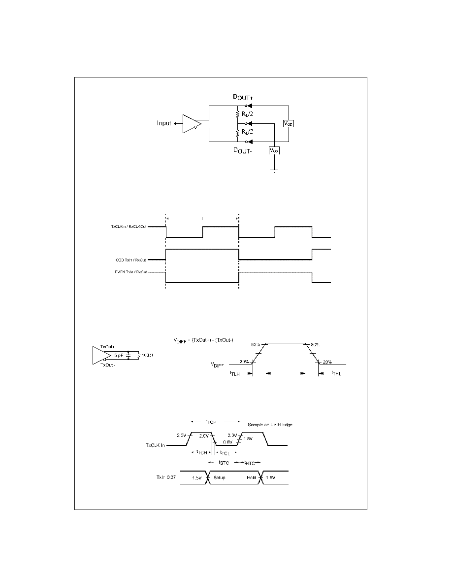
FIGURE 1. Differential LVDS Output DC Test Circuit
AC Loading and Waveforms
Note: The worst case test pattern produces a maximum toggling of digital circuits, LVDS I/O and LVTTL/CMOS I/O. Depending on the valid strobe edge of
transmitter, the TxCLKIn can be either rising or falling edge data strobe.
FIGURE 2. "Worst Case" Test Pattern
FIGURE 3. Transmitter LVDS Output Load and Transition Times
FIGURE 4. Transmitter Setup/Hold and HIGH/LOW Times (Rising Edge Strobe)