Äîêóìåíòàöèÿ è îïèñàíèÿ www.docs.chipfind.ru
© 2005 Fairchild Semiconductor Corporation
DS500864
www.fairchildsemi.com
October 2003
Revised April 2005
FI
N3385
· FI
N3383
· FI
N3384
· FI
N3386
Low V
o
lt
a
ge 28-
Bit
F
l
at
Panel
D
i
spl
ay Li
nk
Seri
ali
z
er
s/Deser
ial
i
z
e
rs
FIN3385 · FIN3383 ·
FIN3384 · FIN3386
Low Voltage 28-Bit Flat Panel Display Link
Serializers/Deserializers
General Description
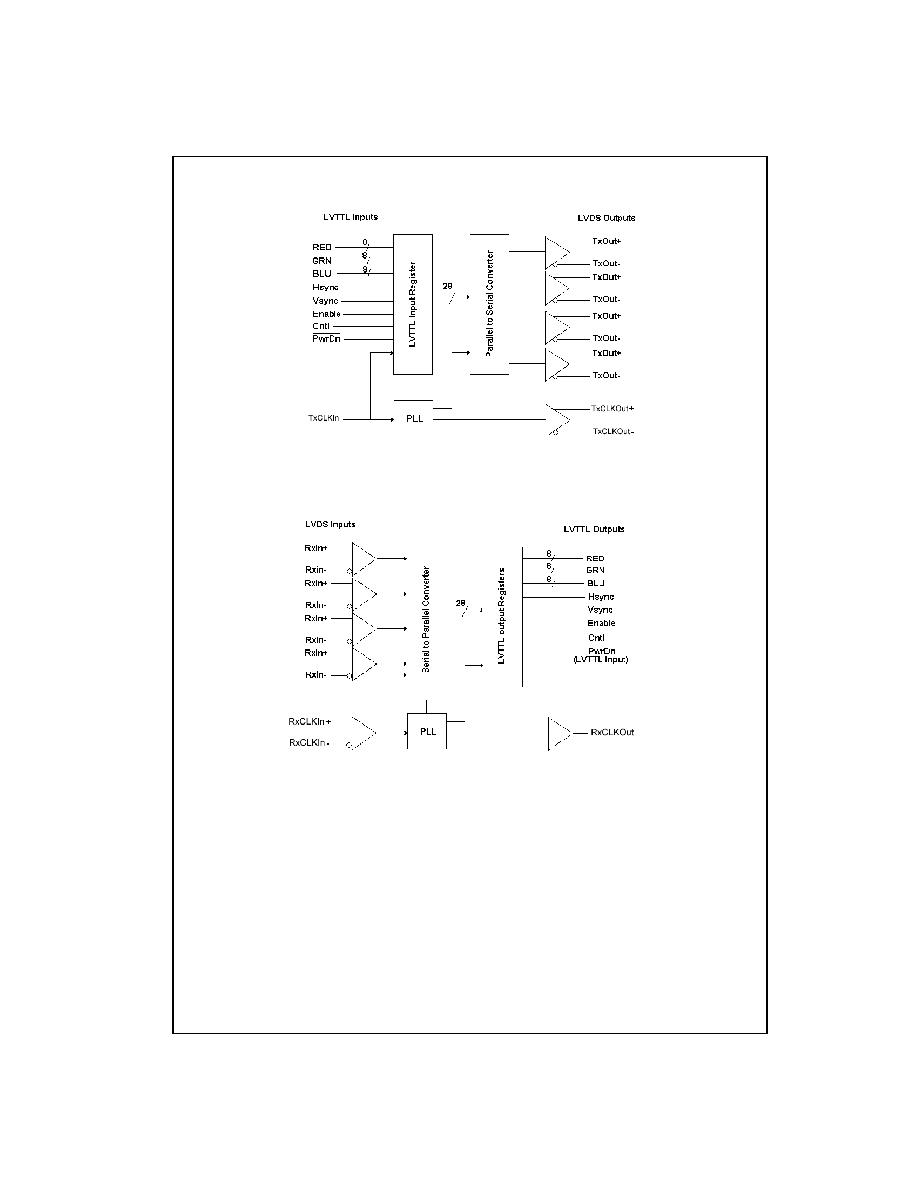
The FIN3385 and FIN3383 transform 28 bit wide parallel
LVTTL (Low Voltage TTL) data into 4 serial LVDS (Low
Voltage Differential Signaling) data streams. A phase-
locked transmit clock is transmitted in parallel with the data
stream over a separate LVDS link. Every cycle of transmit
clock 28 bits of input LVTTL data are sampled and trans-
mitted.
The FIN3386 and FIN3384 receive and convert the 4/3
serial LVDS data streams back into 28/21 bits of LVTTL
data. Refer to Table 1 for a matrix summary of the Serializ-
ers and Deserializers available. For the FIN3385, at a
transmit clock frequency of 85MHz, 28 bits of LVTTL data
are transmitted at a rate of 595Mbps per LVDS channel.
These chipsets are an ideal solution to solve EMI and cable
size problems associated with wide and high-speed TTL
interfaces.
Features
s
Low power consumption
s
20 MHz to 85 MHz shift clock support
s
r
1V common-mode range around 1.2V
s
Narrow bus reduces cable size and cost
s
High throughput (up to 2.38 Gbps throughput)
s
Internal PLL with no external component
s
Compatible with TIA/EIA-644 specification
s
Devices are offered 56-lead TSSOP packages
Ordering Code:
Devices also available in Tape and Reel. Specify by appending suffix letter "X" to the ordering code.
TABLE 1. Display Panel Link Serializers/Deserializers Chip Matrix
Order Number
Package Number
Package Description
FIN3383MTD
MTD56
56-Lead Thin Shrink Small Outline Package (TSSOP), JEDEC MO-153, 6.1mm Wide
FIN3384MTD
MTD56
56-Lead Thin Shrink Small Outline Package (TSSOP), JEDEC MO-153, 6.1mm Wide
FIN3385MTD
MTD56
56-Lead Thin Shrink Small Outline Package (TSSOP), JEDEC MO-153, 6.1mm Wide
FIN3386MTD
MTD56
56-Lead Thin Shrink Small Outline Package (TSSOP), JEDEC MO-153, 6.1mm Wide
Part
CLK Frequency
LVTTL IN
LVDS OUT
LVDS IN
LVTTL OUT
Package
FIN3385
85
28
4
56 TSSOP
FIN3383
66
28
4
56 TSSOP
FIN3386
85
4
28
56 TSSOP
FIN3384
66
4
28
56 TSSOP
www.fairchildsemi.com
2
FIN33
85
·
FIN33
83
·
FIN338
4
·
FIN3386
Block Diagrams
Functional Diagram for FIN3385 and FIN3383
Receiver Functional Diagram for FIN3386 and FIN3384
3
www.fairchildsemi.com
FI
N3385
·
FI
N3383
·
FI
N3384
·
FI
N3386
TRANSMITTERS
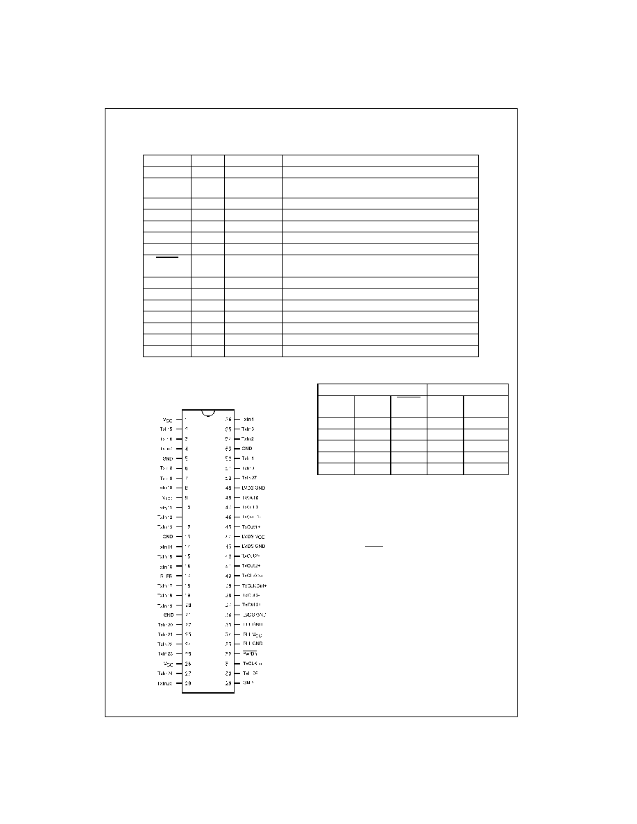
Pin Descriptions
Connection Diagram
FIN3383 and FIN3385 (28:4 Transmitter)
Pin Assignment for TSSOP
Truth Table
H
HIGH Logic Level
L
LOW Logic Level
X
Don't Care
Z
High Impedance
F
Floating
Note 1: The outputs of the transmitter or receiver will remain in a
High Impedance state until V
CC
reaches 2V.
Note 2: TxCLKOut
r
will settle at a free running frequency when the
part is powered up, PwrDn is HIGH and the TxCLKIn is a steady logic
level (L/H/Z).
Pin Names
I/O Type Number of Pins
Description of Signals
TxIn
I
28/21
LVTTL Level Input
TxCLKIn
I
1
LVTTL Level Clock Input
The rising edge is for data strobe.
TxOut
O
4/3
Positive LVDS Differential Data Output
TxOut
O
4/3
Negative LVDS Differential Data Output
TxCLKOut
O
1
Positive LVDS Differential Clock Output
TxCLKOut
O
1
Negative LVDS Differential Clock Output
R_FB
I
1
Rising Edge Clock (HIGH), Falling Edge Clock (LOW)
PwrDn
I
1
LVTTL Level Power-Down Input
Assertion (LOW) puts the outputs in High Impedance state.
PLL V
CC
I
1
Power Supply Pin for PLL
PLL GND
I
2
Ground Pins for PLL
LVDS V
CC
I
1
Power Supply Pin for LVDS Output
LVDS GND
I
3
Ground Pins for LVDS Output
V
CC
I
3
Power Supply Pins for LVTTL Input
GND
I
5
Ground pins for LVTTL Input
NC
No Connect
Inputs
Outputs
TxIn
TxCLKIn
PwrDn
(Note 1)
TxOut
r
TxCLKOut
r
Active
Active
H
L/H
L/H
Active
L/H/Z
H
L/H
X (Note 2)
F
Active
H
L
L/H
F
F
H
L
X (Note 2)
X
X
L
Z
Z
www.fairchildsemi.com
4
FIN33
85
·
FIN33
83
·
FIN338
4
·
FIN3386
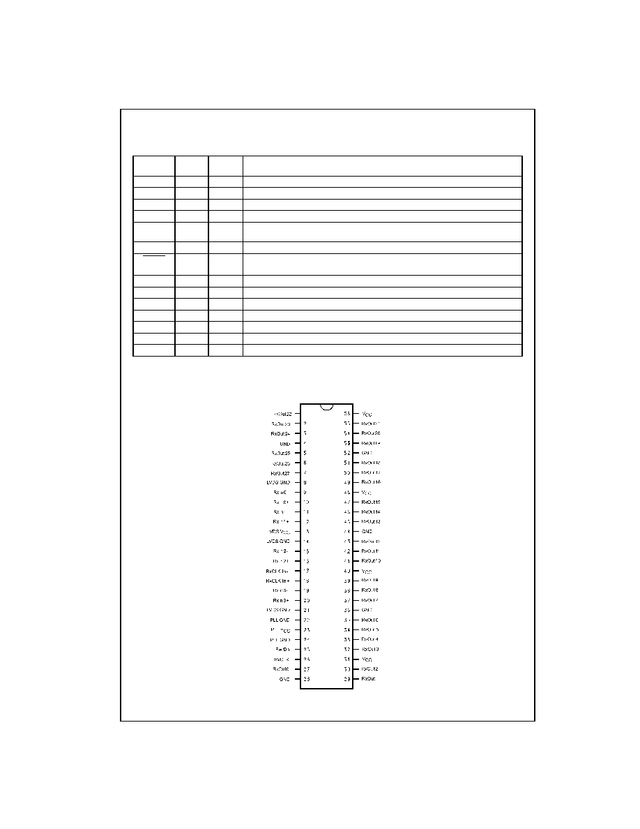
RECEIVERS
Pin Descriptions
Connection Diagram
FIN3386 and FIN3384 (4:28 Receiver)
Pin Assignment for TSSOP
Pin Names I/O Type
Number
of Pins
Description of Signals
RxIn
I
4/3
Negative LVDS Differential Data Input
RxIn
I
4/3
Positive LVDS Differential Data Input
RxCLKIn
I
1
Negative LVDS Differential Clock Input
RxCLKIn
I
1
Positive LVDS Differential Clock Input
RxOut
O
28/21
LVTTL Level Data Output
Goes HIGH for PwrDn LOW
RxCLKOut
O
1
LVTTL Clock Output
PwrDn
I
1
LVTTL Level Input
Refer to Transmitter and Receiver Power-Up and Power-Down Operation Truth Table
PLL V
CC
I
1
Power Supply Pin for PLL
PLL GND
I
2
Ground Pins for PLL
LVDS V
CC
I
1
Power Supply Pin for LVDS Input
LVDS GND
I
3
Ground Pins for LVDS Input
V
CC
I
4
Power Supply for LVTTL Output
GND
I
5
Ground Pin for LVTTL Output
NC
No Connect
5
www.fairchildsemi.com
FI
N3385
·
FI
N3383
·
FI
N3384
·
FI
N3386
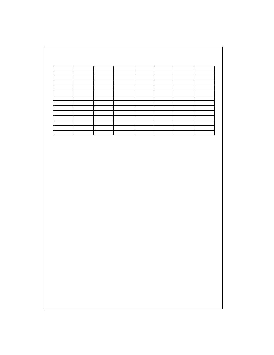
Transmitter and Receiver Power-Up/Power-Down Operation Truth Table
The outputs of the transmitter remain in the High-Impedance state until the power supply reaches 2V. The following table
shows the operation of the transmitter during power-up and power-down and operation of the PwrDn pin.
H
HIGH Logic Level
L
LOW Logic Level
P
Last Valid State
X
Don't Care
Z
High-Impedance
Note 3: If the transmitter is powered up and PwrDn is inactive HIGH and the clock input goes to any state LOW, HIGH, or Z then the internal PLL will go to a
known low frequency and stay until the clock starts normal operation again.
Note 4: If the input is terminated and un-driven (Z) or shorted or open. (fail safe condition)
Note 5: For PwrDn or fail safe condition the RxCLKOut pin will go LOW for Panel Link devices and HIGH for Channel Link devices.
Note 6: Shorted here means (
r
inputs are shorted to each other, or
r
inputs are shorted to each other and Ground or V
CC
, or either
r
inputs are shorted to
Ground or V
CC
) with no other Current/Voltage sources (noise) applied. If the V
ID
is still in the valid range (greater than 100mV) and VCM is in the valid range
(0V to 2.4V) then the input signal is still recognized and the part will respond normally.
Transmitter
PwrDn
Normal
V
CC
2V
!
2V
!
2V
!
2V
!
2V
!
2V
TxIn
X
X
Active
Active
TxOut
Z
Z
Active
X
TxCLKIn
X
X
Active
H/L/Z
TxCLKOut
r
Z
Z
Active
(Note 3)
PwrDn
L
L
H
H
H
H
Receiver
PwrDn
RxIn
r
X
X
Active
Active
(Note 4)
(Note 4)
RxOut
Z
L
L/H
P
H
P
RxCLKIn
r
X
X
Active
(Note 4)
Active
(Note 4)
RxCLKOut
Z
(Note 5)
Active
(Note 5)
(Note 5)
(Note 5)
PwrDn
L
L
H
H
H
H
V
CC
2V
2V
2V
2V
2V
2V