 | –≠–ª–µ–∫—Ç—Ä–æ–Ω–Ω—ã–π –∫–æ–º–ø–æ–Ω–µ–Ω—Ç: FKPF8N80 | –°–∫–∞—á–∞—Ç—å:  PDF PDF  ZIP ZIP |
©2004 Fairchild Semiconductor Corporation
Rev. B1, April 2004
FKPF8N80
Bi-Directional Triode Thyristor Planar Silicon
Absolute Maximum Ratings
T
C
=25
∞
C
unless otherwise noted
Thermal Characteristic
Symbol
Parameter
Rating
Units
V
DRM
Repetitive Peak Off-State Voltage
(Note1 )
800
V
Symbol
Parameter
Conditions
Rating
Units
I
T (RMS)
RMS On-State Current
Commercial frequency, sine full wave 360
∞
conduction, T
C
=91
∞
C
8
A
I
TSM
Surge On-State Current
Sinewave 1 full cycle, peak value,
non-repetitive
50Hz
80
A
60Hz
88
A
I
2
t
I
2
t for Fusing
Value corresponding to 1 cycle of halfwave,
surge on-state current, tp=10ms
32
A
2
s
di/dt
Critical Rate of Rise of On-State Current
I
G
= 2x I
GT
, tr
100ns
50
A/
µ
s
P
GM
Peak Gate Power Dissipation
5
W
P
G (AV)
Average Gate Power Dissipation
0.5
W
V
GM
Peak Gate Voltage
10
V
I
GM
Peak Gate Current
2
A
T
J
Junction Temperature
- 40 ~ 125
∞
C
T
STG
Storage Temperature
- 40 ~ 125
∞
C
V
iso
Isolation Voltage
Ta=25
∞
C, AC 1 minute, T
1
T
2
G terminal to
case
1500
V
Symbol
Parameter
Test Condition
Min.
Typ.
Max.
Units
R
th(J-C)
Thermal Resistance
Junction to case
(Note 4)
-
-
3.6
∞
C/W
FKPF8N80
Application Explanation
∑ Switching mode power supply, light dimmer, electric flasher unit, hair drier
∑ TV sets, stereo, refrigerator, washing machine
∑ Electric blanket, solenoid driver, small motor control
∑ Photo copier, electric tool
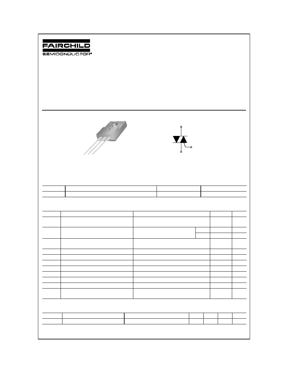
1 2 3
TO-220F
1
2
3
1: T
1
2: T
2
3: Gate
©2004 Fairchild Semiconductor Corporation
Rev. B1, April 2004
FKPF8N80
Electrical Characteristics
T
C
=25
∞
C unless otherwise noted
Notes:
1. Gate Open
2. Measurement using the gate trigger characteristics measurement circuit
3. The critical-rate of rise of the off-state commutating voltage is shown in the table below
4. The contact thermal resistance R
TH(c-f)
in case of greasing is 0.5
∞
C/W
Quadrant Definitions for a Triac
Symbol
Parameter
Test Condition
Min.
Typ.
Max.
Units
I
DRM
Repetieive Peak Off-State Current
V
DRM
applied
-
-
20
µ
A
V
TM
On-State Voltage
T
C
=25
∞
C, I
TM
=12A
Instantaneous measurement
-
-
1.5
V
V
GT
Gate Trigger Voltage
(Note 2)
I
V
D
=12V, R
L
=20
T2(+), Gate (+)
-
-
1.5
V
II
T2(+), Gate (-)
-
-
1.5
V
III
T2(-), Gate (-)
-
-
1.5
V
I
GT
Gate Trigger Current
(Note 2)
I
V
D
=12V, R
L
=20
T2(+), Gate (+)
-
-
30
mA
II
T2(+), Gate (-)
-
-
30
mA
III
T2(-), Gate (-)
-
-
30
mA
V
GD
Gate Non-Trigger Voltage
T
J
=125
∞
C, V
D
=1/2V
DRM
0.2
-
-
V
I
H
Holding Current
V
D
= 12V, I
TM
= 1A
50
mA
I
L
Latching Current
I, III
V
D
= 12V, I
G
= 1.2I
GT
50
mA
II
70
mA
dv/dt
Critical Rate of Rise of
Off-State Voltag
V
DRM
= Rated, T
j
= 125
∞
C,
Exponential Rise
300
V/
µ
s
(dv/dt)
C
Critical-Rate of Rise of Off-State
Commutating Voltage
(Note 3)
10
-
-
V/
µ
s
V
DRM
(V)
Test Condition
Commutating voltage and current waveforms
(inductive load)
FKPF8N80
1. Junction Temperature
T
J
=125
∞
C
2. Rate of decay of on-state
commutating current
(di/dt)
C
= - 4.5A/ms
3. Peak off-state voltage
V
D
= 400V
Supply Voltage
Main Current
Main Voltage
Time
Time
Time
V
D
(dv/dt)
C
(di/dt)
C
T2 Positive
+
-
T2 Negative
Quadrant II
Quadrant I
Quadrant III
Quadrant IV
I
GT
-
+ I
GT
(+) T2
(+) I
GT
GATE
T1
(+) T2
(-) I
GT
GATE
T1
(-) T2
(+) I
GT
GATE
T1
(-) T2
(-) I
GT
GATE
T1

©2004 Fairchild Semiconductor Corporation
Rev. B1, April 2004
FKPF8N80
Typical Curves
Figure 1. Maximum On-state Characteristics
Figure 2. Rated Surge On-state Current
Figure 3. Gate Characteristics
Figure 4. Gate Trigger Current vs Tj
Figure 5. Gate Trigger Voltage vs Tj
Figure 6. Transient Thermal Impedance
0.0
0.5
1.0
1.5
2.0
2.5
0
10
20
30
40
50
125
o
C
25
o
C
O
N
-
S
TA
TE C
U
R
R
E
N
T [
A
]
ON-STATE VOLTAGE [V]
1
10
100
0
10
20
30
40
50
60
70
80
90
100
50Hz
60Hz
PE
AK
S
U
R
G
E O
N
-
S
TA
T
E
C
U
R
R
E
N
T [
A
]
NUMBER OF CYCLES AT 50Hz AND 60Hz
10
100
1000
10000
0.1
1
10
100
V
GD
=0.2V
I
FGT
, I
RGT
I
RGT
V
GT
=1.5V
I
GM
=2A
P
GM
=5W
P
G(AV)
=0.5W
V
GM
=10V
G
A
TE VO
L
T
AG
E [
V
]
GATE CURRENT [mA]
-60
-40
-20
0
20
40
60
80
100
120
140
10
100
1000
I
GT
I
GT
, I
GT
NOR
M
A
L
I
Z
E
D
GA
T
E
T
R
I
GGE
R
CUR
RE
NT
[
%
]
JUNCTION TEMPERATURE [
o
C]
-60
-40
-20
0
20
40
60
80
100
120
140
10
100
1000
N
O
R
M
A
L
IZ
ED
G
A
T
E
T
R
IG
G
E
R
VO
L
T
AG
E
[
%
]
JUNCTION TEMPERATURE [
o
C]
1E-3
0.01
0.1
1
10
100
0.01
0.1
1
10
100
JUNCTION TO CASE
TRA
N
S
I
E
N
T THE
R
MA
L
IMP
E
DA
NCE
R
th
(
j
-
c
)
[
o
C/
W]
TIME [sec]

©2004 Fairchild Semiconductor Corporation
Rev. B1, April 2004
FKPF8N80
Typical Curves
(Continues)
Figure 7. Allowable Ambient Temperature
vs Rms On-state Current
Figure 8. Allowable Case Temperature
vs Rms On-state Current
Figure 9. Maximum On-state Power Dissipation
Figure 10. Repetitive Peak Off-state Current
vs Junction Temperature
Figure 11. Holding Current vs
Junction Temperature
Figure 12. Laching Current vs
Junction Temperature
0
2
4
6
8
10
12
0
20
40
60
80
100
120
140
160
NO HEAT SINK
30 ◊ 30 ◊ 2 mm AL HEAT SINK
50 ◊ 50 ◊ 2 mm AL HEAT SINK
70 ◊ 70 ◊ 2 mm AL HEAT SINK
100 ◊ 100 ◊ 2 mm AL HEAT SINK
MA
X
I
MU
M AL
L
O
W
A
BL
E
A
M
BI
EN
T
T
E
M
P
ER
AT
U
R
E
[
o
C]
RMS ON-STATE CURRENT [A]
0
2
4
6
8
10
12
0
20
40
60
80
100
120
140
160
360
o
CONDUCTION
RESISTIVE,
INDUCTIVE
LOADS
CURVES APPLY REGARDLESS
OF CONDUCTION ANGLE
C
ASE
T
E
MP
ER
ATU
R
E [
o
C]
RMS ON-STATE CURRENT [A]
0
2
4
6
8
10
12
14
16
0
2
4
6
8
10
12
14
16
360
o
CONDUCTION
RESISTIVE,
INDUCTIVE
LOADS
ON
-
S
T
A
T
E
P
O
WE
R
DI
S
S
I
P
A
T
I
O
N
[
W
]
RMS ON-STATE CURRENT [A]
-60
-40
-20
0
20
40
60
80
100
120
140
10
2
10
3
10
4
10
5
TYPICAL EXAMPLE
N
O
R
M
AL
IZ
ED
R
EPE
T
I
VIT
E
O
F
F
-
ST
AT
E
C
U
R
R
E
N
T
[%
]
JUNCTION TEMPERATURE [
o
C]
-60
-40
-20
0
20
40
60
80
100
120
140
10
100
1000
NOR
M
A
L
I
Z
E
D
HOL
D
I
N
G
CUR
RE
NT
[
%
]
JUNCTION TEMPERATURE [
o
C]
-60
-40
-20
0
20
40
60
80
100
120
140
10
100
1000
I
L
, I
L
I
L
N
O
RM
A
L
I
Z
E
D
L
A
T
CHI
N
G
CU
RR
E
N
T
[
%
]
JUNCTION TEMPERATURE [
o
C]

©2004 Fairchild Semiconductor Corporation
Rev. B1, April 2004
FKPF8N80
Typical Curves
(Continues)
Figure 13. Breakover Voltage vs.
Junction Temperature
Figure 14. Gate Trigger Current vs.
Gate Current Pulse Width
Figure 15. Breakover Voltage vs.
Rate of Rise of Off-State Voltage
Figure 16. Commutation Characteristics
-60
-40
-20
0
20
40
60
80
100
120
140
0
20
40
60
80
100
120
140
160
TYPICAL EXAMPLE
N
O
R
M
AL
I
Z
ED
BR
EAKO
VER
V
O
L
T
AG
E
[
%
]
JUNCTION TEMPERATURE [
o
C]
1
10
100
10
100
1000
I
I
I
N
O
R
M
AL
I
Z
ED
GAT
E T
R
I
GGER
C
U
R
R
E
N
T
[
%
]
GATE CURRENT PULSE WIDTH [
µ
s]
10
1
10
2
10
3
10
4
20
40
60
80
100
120
140
160
QUADRANT
QUADRANT
TYPICAL EXAMPLE
Tj=125
N
O
R
M
AL
I
Z
ED
B
R
EA
KO
V
E
R
V
O
L
T
AG
E
[
%
]
RATE OF RISE OF-STATE VOLTAGE [V/
µ
s]
1
10
100
1000
10000
1
10
100
QUADRANT
QUADRANT
TYPICAL
EXAMPLE
T
j
=125
o
C
I
T
=4A
= 500us
V
D
=200V
F=3Hz
C
R
IT
IC
A
L
R
A
T
E
O
F
R
I
S
E
O
F
O
F
F
-
S
T
A
T
E
CO
M
M
UT
A
T
I
O
N V
O
L
T
A
G
E
[
V
/
u
s
]
RATE OF DECAY OF ON-STATE
COMMUTATION CURRENT [A/ms]
©2003 Fairchild Semiconductor Corporation
Rev. B1, April 2004
FKPF8N80
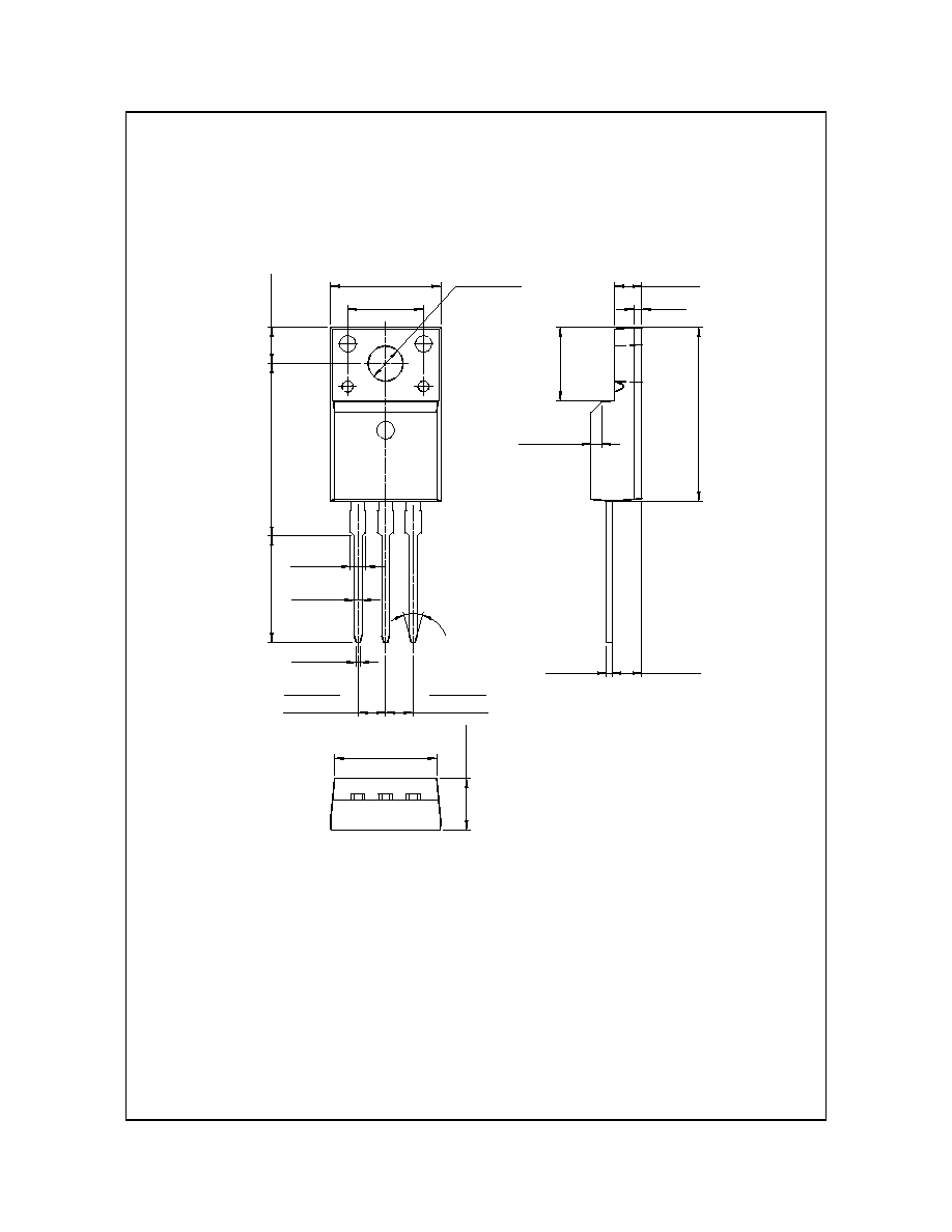
Dimensions in Millimeters
Package Dimension
(7.00)
(0.70)
MAX1.47
(30
∞
)
#1
3.30
±
0.10
15.80
±
0.20
15.87
±
0.20
6.68
±
0.20
9.75
±
0.30
4.70
±
0.20
10.16
±
0.20
(1.00x45
∞
)
2.54
±
0.20
0.80
±
0.10
9.40
±
0.20
2.76
±
0.20
0.35
±
0.10
¯3.18
±
0.10
2.54TYP
[2.54
±
0.20
]
2.54TYP
[2.54
±
0.20
]
0.50
+0.10
≠0.05
TO-220F

DISCLAIMER
FAIRCHILD SEMICONDUCTOR RESERVES THE RIGHT TO MAKE CHANGES WITHOUT FURTHER NOTICE TO ANY
PRODUCTS HEREIN TO IMPROVE RELIABILITY, FUNCTION OR DESIGN. FAIRCHILD DOES NOT ASSUME ANY LIABILITY
ARISING OUT OF THE APPLICATION OR USE OF ANY PRODUCT OR CIRCUIT DESCRIBED HEREIN; NEITHER DOES IT
CONVEY ANY LICENSE UNDER ITS PATENT RIGHTS, NOR THE RIGHTS OF OTHERS.
TRADEMARKS
The following are registered and unregistered trademarks Fairchild Semiconductor owns or is authorized to use and is
not intended to be an exhaustive list of all such trademarks.
LIFE SUPPORT POLICY
FAIRCHILD'S PRODUCTS ARE NOT AUTHORIZED FOR USE AS CRITICAL COMPONENTS IN LIFE SUPPORT
DEVICES OR SYSTEMS WITHOUT THE EXPRESS WRITTEN APPROVAL OF FAIRCHILD SEMICONDUCTOR CORPORATION.
As used herein:
1. Life support devices or systems are devices or
systems which, (a) are intended for surgical implant into
the body, or (b) support or sustain life, or (c) whose
failure to perform when properly used in accordance
with instructions for use provided in the labeling, can be
reasonably expected to result in significant injury to the
user.
2. A critical component is any component of a life
support device or system whose failure to perform can
be reasonably expected to cause the failure of the life
support device or system, or to affect its safety or
effectiveness.
PRODUCT STATUS DEFINITIONS
Definition of Terms
Datasheet Identification
Product Status
Definition
Advance Information
Preliminary
No Identification Needed
Obsolete
This datasheet contains the design specifications for
product development. Specifications may change in
any manner without notice.
This datasheet contains preliminary data, and
supplementary data will be published at a later date.
Fairchild Semiconductor reserves the right to make
changes at any time without notice in order to improve
design.
This datasheet contains final specifications. Fairchild
Semiconductor reserves the right to make changes at
any time without notice in order to improve design.
This datasheet contains specifications on a product
that has been discontinued by Fairchild semiconductor.
The datasheet is printed for reference information only.
Formative or
In Design
First Production
Full Production
Not In Production
ImpliedDisconnectTM
ISOPLANARTM
LittleFETTM
MICROCOUPLERTM
MicroFETTM
MicroPakTM
MICROWIRETM
MSXTM
MSXProTM
OCXTM
OCXProTM
OPTOLOGIC
OPTOPLANARTM
FACT Quiet SeriesTM
FAST
FASTrTM
FPSTM
FRFETTM
GlobalOptoisolatorTM
GTOTM
HiSeCTM
I
2
CTM
i-LoTM
Rev. I10
ACExTM
ActiveArrayTM
BottomlessTM
CoolFETTM
CROSSVOLTTM
DOMETM
EcoSPARKTM
E
2
CMOSTM
EnSignaTM
FACTTM
PACMANTM
POPTM
Power247TM
PowerSaverTM
PowerTrench
QFET
QSTM
QT OptoelectronicsTM
Quiet SeriesTM
RapidConfigureTM
RapidConnectTM
SILENT SWITCHER
SMART STARTTM
SPMTM
StealthTM
SuperFETTM
SuperSOTTM-3
SuperSOTTM-6
SuperSOTTM-8
SyncFETTM
TinyLogic
TINYOPTOTM
TruTranslationTM
UHCTM
UltraFET
VCXTM
Across the board. Around the world.TM
The Power Franchise
Programmable Active DroopTM