 | –≠–ª–µ–∫—Ç—Ä–æ–Ω–Ω—ã–π –∫–æ–º–ø–æ–Ω–µ–Ω—Ç: FM24C64L | –°–∫–∞—á–∞—Ç—å:  PDF PDF  ZIP ZIP |

1
www.fairchildsemi.com
FM24C64 Rev. C
FM24C64 ≠ 64K-Bit Standard 2-Wire Bus Interface Serial EEPROM
December 2001
© 2001 Fairchild Semiconductor Corporation
FM24C64 ≠ 64K-Bit Standard 2-Wire Bus
Interface Serial EEPROM
General Description
FM24C64 is a 64Kbit CMOS non-volatile serial EEPROM orga-
nized as 8K x 8 bit memory. This device confirms to Extended IIC
2-wire protocol that allows accessing of memory in excess of
16Kbit on an IIC bus. This serial communication protocol uses a
Clock signal (SCL) and a Data signal (SDA) to synchronously
clock data between a master (e.g. a microcontroller) and a slave
(EEPROM). FM24C64 is designed to minimize pin count and
simplify PC board layout requirements.
FM24C64 offers hardware write protection where by the entire
memory array can be write protected by connecting WP pin to V
CC
.
This section of memory then becomes unalterable until the WP pin
is switched to V
SS
.
"LZ" and "L" versions of FM24C64 offer very low standby current
making them suitable for low power applications. This device is
offered in SO, TSSOP and DIP packages.
Fairchild EEPROMs are designed and tested for applications
requiring high endurance, high reliability and low power consump-
tion.
Block Diagram
Features
I Extended operating voltage: 2.5V to 5.5V
I Up to 400 KHz clock frequency at 2.5V to 5.5V
I Low power consumption
-- 0.5mA active current typical
-- 10
µA standby current typical
-- 1
µA standby current typical (L version)
-- 0.1
µA standby current typical (LZ version)
I Schmitt trigger inputs
I 32 byte page write mode
I Self timed write cycle (6ms typical)
I Hardware Write Protection for the entire array
I Endurance: up to 100K data changes
I Data Retention: Greater than 40 years
I Packages: 8-Pin DIP, 8-Pin SO and 8-Pin TSSOP
I Temperature range
-- Commercial: 0
∞C to +70∞C
-- Industrial (E): -40
∞C to +85∞C
-- Automotive (V): -40
∞C to +125∞C
H.V. GENERATION
TIMING &CONTROL
E2PROM
ARRAY
YDEC
DATA REGISTER
XDEC
CONTROL
LOGIC
WORD
ADDRESS
COUNTER
SLAVE ADDRESS
REGISTER &
COMPARATOR
START
STOP
LOGIC
WRITE
LOCKOUT
CK
DIN
R/W
SDA
SCL
WP
VCC
VSS
DOUT
A2
A1
A0
2
www.fairchildsemi.com
FM24C64 Rev. C
FM24C64 ≠ 64K-Bit Standard 2-Wire Bus Interface Serial EEPROM
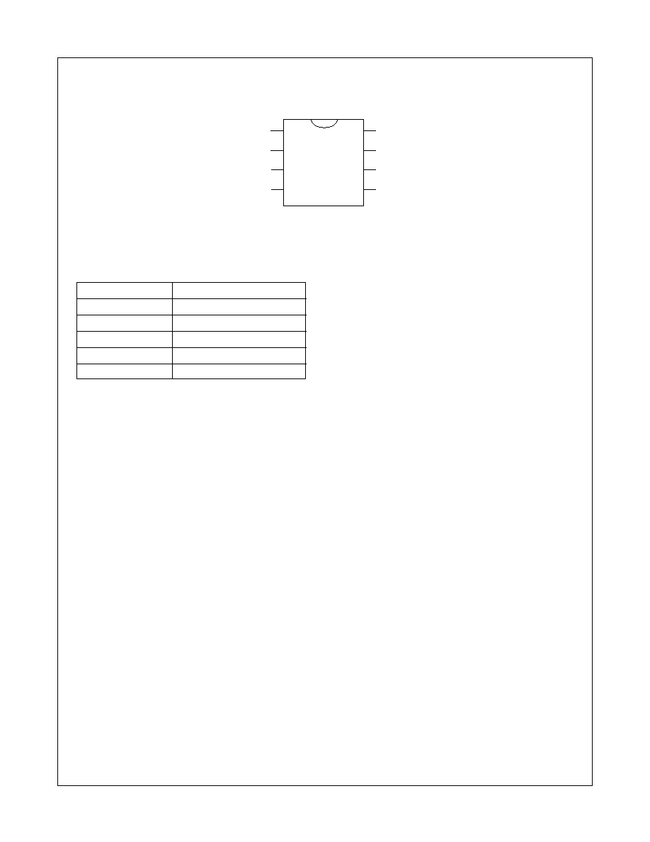
A0
A1
A2
V
SS
V
CC
WP
SCL
SDA
8
7
6
5
1
2
3
4
FM24C64
Connection Diagram
Dual-in-Line Package (N), SO Package (M8) and TSSOP Package (MT8)
See Package Number N08E, M08A and MTC08
Pin Names
V
SS
Ground
SDA
Serial Data I/O
SCL
Serial Clock Input
WP
Write Protect
V
CC
Power Supply
A0, A1, A2
Device Address Inputs

3
www.fairchildsemi.com
FM24C64 Rev. C
FM24C64 ≠ 64K-Bit Standard 2-Wire Bus Interface Serial EEPROM
Ordering Information
FM
24
C
XX
F
LZ
E
YY
X
Letter
Description
Blank
Tube
X
Tape and Reel
Package
N
8-pin DIP
M8
8-pin SOIC
MT8
8-pin TSSOP
Temp. Range
Blank
0 to 70
∞C
E
-40 to +85
∞C
V
-40 to +125
∞C
Voltage Operating Range
Blank
4.5V to 5.5V
L
2.5V to 5.5V
LZ
2.5V to 5.5V and
<1
µA Standby Current
SCL Clock Frequency
Blank
100KHz
F
400KHz
Density
64
64K with write protect
C
CMOS
Interface
24
IIC - 2 Wire
FM
Fairchild Non-Volatile
Memory

4
www.fairchildsemi.com
FM24C64 Rev. C
FM24C64 ≠ 64K-Bit Standard 2-Wire Bus Interface Serial EEPROM
Product Specifications
Absolute Maximum Ratings
Ambient Storage Temperature
≠65
∞C to +150∞C
All Input or Output Voltages
with Respect to Ground
6.5V to ≠0.3V
Lead Temperature
(Soldering, 10 seconds)
+300
∞C
ESD Rating
2000V min.
Operating Conditions
Ambient Operating Temperature
FM24C64
0
∞C to +70∞C
FM24C64E
-40
∞C to +85∞C
FM24C64V
-40
∞C to +125∞C
Positive Power Supply
FM24C64
4.5V to 5.5V
FM24C64L
2.5V to 5.5V
FM24C64LZ
2.5V to 5.5V
Standard V
CC
(4.5V to 5.5V) DC Electrical Characteristics
Symbol
Parameter
Test Conditions
Limits
Units
Min
Typ
Max
(Note 1)
I
CCA
Active Power Supply Current
f
SCL
= 400 KHz
0.5
1.0
mA
f
SCL
= 100 KHz
I
SB
Standby Current
V
IN
= GND or V
CC
10
50
µA
I
LI
Input Leakage Current
V
IN
= GND to V
CC
0.1
1
µA
I
LO
Output Leakage Current
V
OUT
= GND to V
CC
0.1
1
µA
V
IL
Input Low Voltage
≠0.3
V
CC
x 0.3
V
V
IH
Input High Voltage
V
CC
x 0.7
V
CC
+ 0.5
V
V
OL
Output Low Voltage
I
OL
= 2.1 mA
0.4
V
Low V
CC
(2.5V to 5 .5V) DC Electrical Characteristics
Symbol
Parameter
Test Conditions
Limits
Units
Min
Typ
Max
(Note 1)
I
CCA
Active Power Supply Current
f
SCL
= 400 KHz
0.5
1.0
mA
f
SCL
= 100 KHz
I
SB
Standby Current
V
IN
= GND
V
CC
= 2.5V - 4.5V (L)
1
10
µA
(Note 3)
or V
CC
V
CC
= 2.5V - 4.5V (LZ)
0.1
1
µA
V
CC
= 4.5V - 5.5V
10
50
µA
I
LI
Input Leakage Current
V
IN
= GND to V
CC
0.1
1
µA
I
LO
Output Leakage Current
V
OUT
= GND to V
CC
0.1
1
µA
V
IL
Input Low Voltage
≠0.3
V
CC
x 0.3
V
V
IH
Input High Voltage
V
CC
x 0.7
V
CC
+ 0.5
V
V
OL
Output Low Voltage
I
OL
= 2.1 mA
0.4
V
Capacitance
T
A
= +25
∞C, f = 100/400 KHz, V
CC
= 5V
(Note 2)
Symbol
Test
Conditions
Max
Units
C
I/O
Input/Output Capacitance (SDA)
V
I/O
= 0V
8
pF
C
IN
Input Capacitance (A0, A1, A2, SCL)
V
IN
= 0V
6
pF
Note 1: Typical values are T
A
= 25
∞C and nominal supply voltage (5V).
Note 2: This parameter is periodically sampled and not 100% tested.
Note 3: The "L" and "LZ" versions can be operated in the 2.5V to 5.5V V
CC
range. However the I
SB
values for L and LZ are applicable only when V
CC
is in the 2.5V to 4.5V range.

5
www.fairchildsemi.com
FM24C64 Rev. C
FM24C64 ≠ 64K-Bit Standard 2-Wire Bus Interface Serial EEPROM
AC Test Conditions
Input Pulse Levels
V
CC
x 0.1 to V
CC
x 0.9
Input Rise and Fall Times
10 ns
Input & Output Timing Levels
V
CC
x 0.3 to V
CC
x 0.7
Output Load
1 TTL Gate and C
L
= 100 pF
Bus Timing
SCL
SDA
IN
SDA
OUT
tF
tLOW
tHIGH
tR
tLOW
tAA
tDH
tBUF
tSU:STA
tHD:DAT
tHD:STA
tSU:DAT
tSU:STO
0.9V
CC
0.1V
CC
0.7V
CC
0.3V
CC
Read and Write Cycle Limits (Standard and Low V
CC
Range 2.5V - 5.5V)
Symbol
Parameter
100 KHz
400 KHz
Units
Min
Max
Min
Max
f
SCL
SCL Clock Frequency
100
400
KHz
T
I
Noise Suppression Time Constant at
SCL, SDA Inputs (Minimum V
IN
100
50
ns
Pulse width)
t
AA
SCL Low to SDA Data Out Valid
0.3
3.5
0.1
0.9
µs
t
BUF
Time the Bus Must Be Free before
4.7
1.3
µs
a New Transmission Can Start
t
HD:STA
Start Condition Hold Time
4.0
0.6
µs
t
LOW
Clock Low Period
4.7
1.5
µs
t
HIGH
Clock High Period
4.0
0.6
µs
t
SU:STA
Start Condition Setup Time
4.7
0.6
µs
(for a Repeated Start Condition)
t
HD:DAT
Data in Hold Time
0
0
ns
t
SU:DAT
Data in Setup Time
250
120
ns
t
R
SDA and SCL Rise Time
1
0.3
µs
t
F
SDA and SCL Fall Time
300
300
ns
t
SU:STO
Stop Condition Setup Time
4.7
0.6
µs
t
DH
Data Out Hold Time
100
50
n s
t
WR
Write Cycle Time
6
6
m s
Note 4: The write cycle time (t
WR
) is the time from a valid stop condition of a write sequence to the end of the internal erase/program cycle. During the write cycle,
the FM24C64 bus interface circuits are disabled, SDA is allowed to remain high per the bus-level pull-up resistor, and the device does not respond to its slave
address. Refer "Write Cycle Timing" diagram.
AC Testing Input/Output Waveforms