Äîêóìåíòàöèÿ è îïèñàíèÿ www.docs.chipfind.ru

1
www.fairchildsemi.com
FM27C256 262,144-Bit (32K x 8) High Performance CMOS EPROM
www.fairchildsemi.com
FM27C256
FM27C256
262,144-Bit (32K x 8) High Performance CMOS EPROM
General Description
The FM27C256 is a 256K Electrically Programmable Read Only
Memory. It is manufactured in Fairchild's latest CMOS split gate
EPROM technology which enables it to operate at speeds as fast
as 90 ns access time over the full operating range.
The FM27C256 provides microprocessor-based systems exten-
sive storage capacity for large portions of operating system and
application software. Its 90 ns access time provides high speed
operation with high-performance CPUs. The FM27C256 offers a
single chip solution for the code storage requirements of 100%
firmware-based equipment. Frequently-used software routines
are quickly executed from EPROM storage, greatly enhancing
system utility.
The FM27C256 is configured in the standard EPROM pinout
which provides an easy upgrade path for systems which are
currently using standard EPROMs.
Block Diagram
January 2000
The FM27C256 is one member of a high density EPROM Family
which range in densities up to 4 Mb.
Features
I High performance CMOS
-- 90 ns access time
I JEDEC standard pin configuration
-- 28-pin PDIP package
-- 32-pin chip carrier
-- 28-pin CERDIP package
I Drop-in replacement for 27C256 or 27256
I Manufacturer's identification code
DS800034-1
Output Enable
and Chip Enable Logic
Y Decoder
X Decoder
. .
. . . . . . .
Output
Buffers
Y Gating
Data Outputs O0 - O7
VCC
GND
VPP
OE
CE/PGM
A0 - A14
Address
Inputs
© 1998 Fairchild Semiconductor Corporation
2
www.fairchildsemi.com
FM27C256 262,144-Bit (32K x 8) High Performance CMOS EPROM
www.fairchildsemi.com
FM27C256
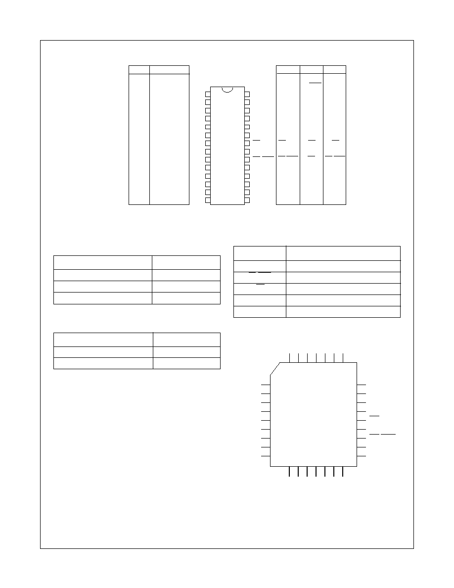
Connection Diagrams
Commercial Temp. Range (0
°
C to +70
°
C)
V
CC
= 5V
±
10%
Parameter/Order Number
Access Time (ns)
FM27C256 Q, N, V 90
90
FM27C256 Q, N, V 120
120
FM27C256 Q, N, V 150
150
Extended Temp. Range (-40
°
C to +85
°
C)
V
CC
= 5V
±
10%
Parameter/Order Number
Access Time (ns)
FM27C256 QE, NE, VE 120
120
FM27C256 QE, NE, VE 150
150
Note: Surface mount PLCC package available for commercial and extended
temperature ranges only.
Package Types: FM27C256 Q, N, V XXX
Q = Quartz-Windowed Ceramic DIP
N = Plastic OTP DIP
V = Surface-Mount PLCC
· All Packages conform to the JEDEC standard.
· All versions are guaranteed to function for slower speeds.
Pin Names
Symbol
Description
A0A14
Addresses
CE/PGM
Chip Enable/Program
OE
Output Enable
O0O7
Outputs
XX
Don't Care (during Read)
PLCC
Note: Compatible EPROM pin configurations are shown in the blocks adjacent to the FM27C256 pins.
A
8
A
9
A
11
XX
OE
A
10
CE/PGM
O
7
O
6
A
6
A
5
A
4
A
3
A
2
A
1
A
0
XX
O
0
A
7
A
12
V
PP
XX
V
CC
A
14
A
13
O
1
O
2
GND
XX
O
3
O
4
O
5
5
6
7
8
9
10
11
12
13
29
28
27
26
25
24
23
22
21
14 15 16 17 18 19 20
4 3 2 1 32 31 30
DS800034-2
DS800034-3
1
2
3
4
5
6
7
8
9
10
11
12
13
14
28
27
26
25
24
23
22
21
20
19
18
17
16
15
V
PP
A12
A7
A6
A5
A4
A3
A2
A1
A0
O0
O1
O2
GND
27C040
27C040
XX/VPP
A16
A15
A12
A7
A6
A5
A4
A3
A2
A1
A0
O0
O1
O2
GND
DlP
FM27C256
V
CC
A14
A13
A8
A9
A11
OE
A10
CE/PGM
O7
O6
O5
O4
O3
A15
A12
A7
A6
A5
A4
A3
A2
A1
A0
O0
O1
O2
GND
27C512
27C512
XX/VPP
A16
A15
A12
A7
A6
A5
A4
A3
A2
A1
A0
O0
O1
O2
GND
27C010
27C010
VCC
A18
A17
A14
A13
A8
A9
A11
OE
A10
CE/PGM
O7
O6
O5
O4
O3
VCC
XX/PGM
XX
A14
A13
A8
A9
A11
OE
A10
CE
O7
O6
O5
O4
O3
VCC
A14
A13
A8
A9
A11
OE/VPP
A10
CE/PGM
O7
O6
O5
O4
O3
Top
3
www.fairchildsemi.com
FM27C256 262,144-Bit (32K x 8) High Performance CMOS EPROM
www.fairchildsemi.com
FM27C256
Absolute Maximum Ratings
(Note 1)
Storage Temperature
-65
°C to +150°C
All Input Voltages except A9 with
Respect to Ground
-0.6V to +7V
V
PP
and A9 with Respect
to Ground
-0.7V to +14V
V
CC
Supply Voltage with
Respect to Ground
-0.6V to +7V
ESD Protection
> 2000V
All Output Voltages with
Respect to Ground
V
CC
+ 1.0V to GND -0.6V
Operating Range
Range
Temperature
V
CC
Comm'l
0
°C to +70°C
+5V
±10%
Industrial
-40
°C to +85°C
+5V
±10%
Read Operation
DC Electrical Characteristics
Over Operating Range with V
PP
= V
CC
Symbol
Parameter
Test Conditions
Min
Max
Units
V
IL
Input Low Level
-0.5
0.8
V
V
IH
Input High Level
2.0
V
CC
+1
V
V
OL
Output Low Voltage
I
OL
= 2.1 mA
0.4
V
V
OH
Output High Voltage
I
OH
= -2.5 mA
3.5
V
I
SB1
V
CC
Standby Current
CE = V
CC
±0.3V
100
µA
(Note 11)
(CMOS)
I
SB2
V
CC
Standby Current (TTL)
CE = V
IH
1
mA
I
CC1
V
CC
Active Current
CE = OE = V
IL
,f=5 MHz
35
mA
TTL Inputs
Inputs = V
IH
or V
IL
, I/O = 0 mA
I
PP
V
PP
Supply Current
V
PP
= V
CC
10
µA
V
PP
V
PP
Read Voltage
V
CC
- 0.7
V
CC
V
I
LI
Input Load Current
V
IN
= 5.5V or GND
-1
1
µA
I
LO
Output Leakage Current
V
OUT
= 5.5V or GND
-10
10
µA
AC Electrical Characteristics
Over Operating Range with V
PP
= V
CC
Symbol
Parameter
90
100
120
150
200
Units
MinMax MinMax MinMax MinMax MinMax
t
ACC
Address to Output Delay
90
100
120
150
200
ns
t
CE
CE to Output Delay
90
100
120
150
200
t
OE
OE to Output Delay
35
50
50
50
50
t
DF
Output Disable to
30
30
35
45
45
(Note 2)
Output Float
t
OH
Output Hold from
0
0
0
0
0
(Note 2)
Addresses,
CE or OE, Whichever
Occurred First
Capacitance
(Note 2) T
A
= +25°C, f = 1 MHz
Symbol
Parameter
Conditions
Typ Max
Units
C
IN
Input Capacitance
V
IN
= 0V
6
12
pF
C
OUT
Output Capacitance
V
OUT
= 0V
9
12
pF
4
www.fairchildsemi.com
FM27C256 262,144-Bit (32K x 8) High Performance CMOS EPROM
www.fairchildsemi.com
FM27C256
AC Test Conditions
Output Load
1 TTL Gate and CL = 100 pF (Note 8)
Input Rise and Fall Times
5 ns
Input Pulse Levels
0.45 to 2.4V
Timing Measurement Reference Level (Note 10)
Inputs
0.8V and 2.0V
Outputs
0.8V and 2.0V
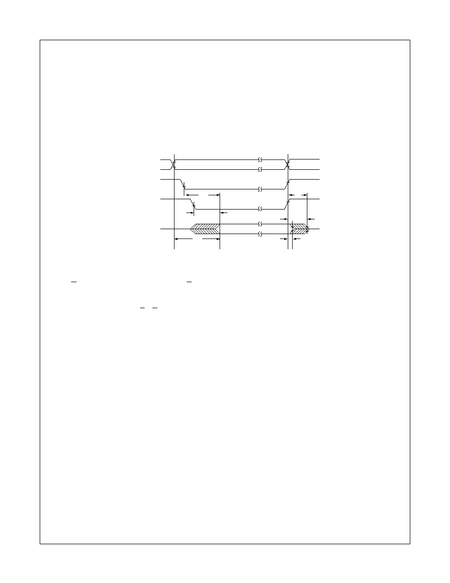
AC Waveforms
(Note 6) (Note 7) (Note 9)
Note 1: Stresses above those listed under "Absolute Maximum Ratings" may cause permanent damage to the device. This is stress rating only and functional operation of the
device at these or any other conditions above those indicated in the operational sections of this specification is not implied. Exposure to absolute maximum rating conditions for
extended periods may affect device reliability.
Note 2: This parameter is only sampled and is not 100% tested.
Note 3: OE may be delayed up to t
ACC
- t
OE
after the falling edge of CE without impacting t
ACC
.
Note 4: The t
DF
and t
CF
compare level is determined as follows:
High to TRI-STATE
®
, the measured V
OH1
(DC) - 0.10V;
Low to TRI-STATE, the measured V
OL1
(DC) + 0.10V.
Note 5: TRI-STATE may be attained using OE or CE.
Note 6: The power switching characteristics of EPROMs require careful device decoupling. It is recommended that at least a 0.1
µF ceramic capacitor be used on every device
between V
CC
and GND.
Note 7: The outputs must be restricted to V
CC
+ 1.0V to avoid latch-up and device damage.
Note 8: TTL Gate: I
OL
= 1.6 mA, I
OH
= -400
µA.
C
L
= 100 pF includes fixture capacitance.
Note 9: V
PP
may be connected to V
CC
except during programming.
Note 10: Inputs and outputs can undershoot to -2.0V for 20 ns Max.
Note 11: CMOS inputs: V
IL
= GND
±0.3V, V
IH
= V
CC
±0.3V.
ADDRESSES VALID
VALID OUTPUT
Hi-Z
Hi-Z
2.0V
0.8V
2.0V
0.8V
2.0V
0.8V
2.0V
0.8V
ADDRESSES
CE
OE
OUTPUT
t
OE
(Note 3)
t
ACC
(Note 3)
t
CE
t
CE
(Notes 4, 5)
t
OH
t
DF
(Notes 4, 5)
DS800034-4
5
www.fairchildsemi.com
FM27C256 262,144-Bit (32K x 8) High Performance CMOS EPROM
www.fairchildsemi.com
FM27C256
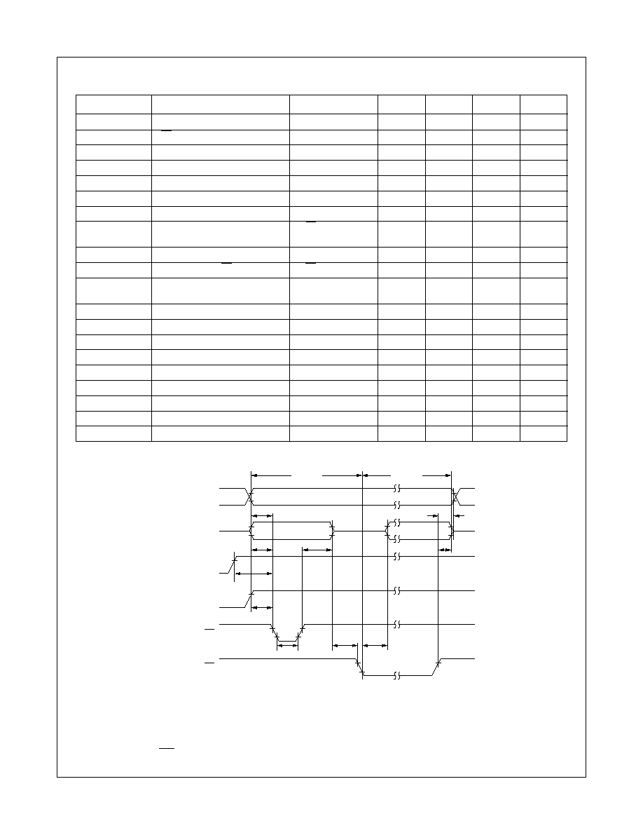
Programming Characteristics
(Note 12) (Note 13) (Note 14) (Note 15)
Symbol
Parameter
Conditions
Min
Typ
Max
Units
t
AS
Address Setup Time
1
µs
t
OES
OE Setup Time
1
µs
t
VPS
V
PP
Setup Time
1
µs
t
VCS
V
CC
Setup Time
1
µs
t
DS
Data Setup Time
1
µs
t
AH
Address Hold Time
0
µs
t
DH
Data Hold Time
1
µs
t
DF
Output Enable to Output
CE = V
IL
0
60
ns
Float Delay
t
PW
Program Pulse Width
45
50
105
µs
t
OE
Data Valid from OE
CE = V
IL
100
ns
I
PP
V
PP
Supply Current
CE = V
IL
30
mA
during Programming Pulse
I
CC
V
CC
Supply Current
50
mA
T
A
Temperature Ambient
20
25
30
°C
V
CC
Power Supply Voltage
6.25
6.5
6.75
V
V
PP
Programming Supply Voltage
12.5
12.75
13.0
V
t
FR
Input Rise, Fall Time
5
ns
V
IL
Input Low Voltage
0.0
0.45
V
V
IH
Input High Voltage
2.4
4.0
V
t
IN
Input Timing Reference Voltage
0.8
2.0
V
t
OUT
Output Timing Reference Voltage
0.8
2.0
V
Programming Waveforms
(Note 14)
Note 12: Fairchild's standard product warranty applies to devices programmed to specifications described herein.
Note 13: V
CC
must be applied simultaneously or before V
PP
and removed simultaneously or after V
PP
. The EPROM must not be inserted into or removed from a board with
voltage applied to V
PP
or V
CC
.
Note 14: The maximum absolute allowable voltage which may be applied to the V
PP
pin during programming is 14V. Care must be taken when switching the V
PP
supply to
prevent any overshoot from exceeding this 14V maximum specification. At least a 0.1
µF capacitor is required across V
PP
, V
CC
to GND to suppress spurious voltage transients
which may damage the device.
Note 15: During power up the PGM pin must be brought high (
V
IH
) either coincident with or before power is applied to V
PP
.
ADDRESS N
DATA IN STABLE
ADD N
DATA OUT VALID
ADD N
2.0V
0.8V
2.0V
0.8V
5.25V
12.75V
2.0V
0.8V
2.0V
0.8V
ADDRESSES
DATA
CE
V
PP
V
CC
OE
t
OE
t
OES
t
PW
t
VPS
t
VCS
t
DS
t
AS
t
AH
t
DF
t
DH
PROGRAM
PROGRAM
VERIFY
DS800034-5
6
www.fairchildsemi.com
FM27C256 262,144-Bit (32K x 8) High Performance CMOS EPROM
www.fairchildsemi.com
FM27C256
Turbo Programming Algorithm Flow Chart
V
CC
= 6.5V V
PP
= 12.75V
n = 0
ADDRESS = FIRST LOCATION
CHECK ALL BYTES
1ST: V
CC
= V
PP
= 6.0V
2ND: V
CC
= V
PP
= 4.3V
PROGRAM ONE 50
µs PULSE
INCREMENT n
ADDRESS = FIRST LOCATION
VERIFY
BYTE
n = 10?
DEVICE
FAILED
LAST
ADDRESS
?
INCREMENT
ADDRESS
n = 0
PROGRAM ONE
50
µs
PULSE
INCREMENT
ADDRESS
VERIFY
BYTE
LAST
ADDRESS
?
PASS
NO
FAIL
YES
YES
PASS
NO
FAIL
NO
YES
DS800034-6
Note:
The standard National Semiconductor algorithm may also be used but it will have longer programming time.
FIGURE 1.

7
www.fairchildsemi.com
FM27C256 262,144-Bit (32K x 8) High Performance CMOS EPROM
www.fairchildsemi.com
FM27C256
Functional Description
DEVICE OPERATION
The six modes of operation of the EPROM are listed in Table 1. It
should be noted that all inputs for the six modes are at TTL levels.
The power supplies required are V
CC
and V
PP
. The V
PP
power
supply must be at 12.75V during the three programming modes,
and must be at 5V in the other three modes. The V
CC
power supply
must be at 6.5V during the three programming modes, and at 5V
in the other three modes.
Read Mode
The EPROM has two control functions, both of which must be
logically active in order to obtain data at the outputs. Chip Enable
(CE/PGM) is the power control and should be used for device
selection. Output Enable (OE) is the output control and should be
used to gate data to the output pins, independent of device
selection. Assuming that addresses are stable, address access
time (t
ACC
) is equal to the delay from CE to output (t
CE
). Data is
available at the outputs t
OE
after the falling edge of OE, assuming
that CE/PGM has been low and addresses have been stable for
at least t
ACC
t
OE
.
Standby Mode
The EPROM has a standby mode which reduces the active power
dissipation by over 99%, from 385 mW to 0.55 mW. The EPROM
is placed in the standby mode by applying a CMOS high signal to
the CE/PGM input. When in standby mode, the outputs are in a
high impedance state, independent of the OE input.
Output Disable
The EPROM is placed in output disable by applying a TTL high
signal to the OE input. When in output disable all circuitry is
enabled, except the outputs are in a high impedance state (TRI-
STATE).
Output OR-Typing
Because the EPROM is usually used in larger memory arrays,
Fairchild has provided a 2-line control function that accommo-
dates this use of multiple memory connections. The 2-line control
function allows for:
1. the lowest possible memory power dissipation, and
2. complete assurance that output bus contention will not
occur.
To most efficiently use these two control lines, it is recommended
that CE/PGM be decoded and used as the primary device select-
ing function, while OE be made a common connection to all
devices in the array and connected to the READ line from the
system control bus. This assures that all deselected memory
devices are in their low power standby modes and that the output
pins are active only when data is desired from a particular memory
device.
Programming
CAUTION: Exceeding 14V on pin 1 (V
PP
) will damage the EPROM.
Initially, and after each erasure, all bits of the EPROM are in the
"1's" state. Data is introduced by selectively programming "0's"
into the desired bit locations. Although only "0's" will be pro-
grammed, both "1's" and "0's" can be presented in the data word.
The only way to change a "0" to a "1" is by ultraviolet light erasure.
The EPROM is in the programming mode when the V
PP
power
supply is at 12.75V and OE is at V
IH
. It is required that at least a
0.1
µF capacitor be placed across V
PP
, V
CC
to ground to suppress
spurious voltage transients which may damage the device. The
data to be programmed is applied 8 bits in parallel to the data
output pins. The levels required for the address and data inputs
are TTL.
When the address and data are stable, an active low, TTL program
pulse is applied to the CE/PGM input. A program pulse must be
applied at each address location to be programmed. The EPROM
is programmed with the Turbo Programming Algorithm shown in
Figure 1. Each Address is programmed with a series of 50
µs
pulses until it verifies good, up to a maximum of 10 pulses. Most
memory cells will program with a single 50
µs pulse. (The standard
National Semiconductor Algorithm may also be used but it will
have longer programming time.)
The EPROM must not be programmed with a DC signal applied to
the CE/PGM input.
Programming multiple EPROM in parallel with the same data can
be easily accomplished due to the simplicity of the programming
requirments. Like inputs of the parallel EPROM may be connected
together when they are programmed with the same data. A low
level TTL pulse applied to the CE/PGM input programs the
paralleled EPROM.
Program Inhibit
Programming multiple EPROMs in parallel with different data is
also easily accomplished. Except for CE/PGM, all like inputs
(including OE) of the parallel EPROMs may be common. A TTL
low level program pulse applied to an EPROM's CE/PGM input
with V
PP
at 12.75V will program that EPROM. A TTL high level CE/
PGM input inhibits the other EPROMs from being programmed.
Program Verify
A verify should be performed on the programmed bits to determine
whether they were correctly programmed. The verify may be
performed with V
PP
at 12.75V. V
PP
must be at V
CC
, except during
programming and program verify.
AFTER PROGRAMMING
Opaque labels should be placed over the EPROM window to
prevent unintentional erasure. Covering the window will also
prevent temporary functional failure due to the generation of photo
currents.
MANUFACTURER'S IDENTIFICATION CODE
The EPROM has a manufacturer's identification code to aid in
programming. When the device is inserted in an EPROM pro-
grammer socket, the programmer reads the code and then
automatically calls up the specific programming algorithm for the
part. This automatic programming control is only possible with
programmers which have the capability of reading the code.
The Manufacturer's Identification code, shown in Table 2, specifi-
cally identifies the manufacturer and device type. The code for
FM27C256 is "8F04", where "8F" designates that it is made by
Fairchild Semiconductor, and "04" designates a 256K part.
The code is accessed by applying 12V
±0.5V to address pin A9.
Addresses A1A8, A10A16, and all control pins are held at V
IL
.
Address pin A0 is held at V
IL
for the manufacturer's code, and held
at V
IH
for the device code. The code is read on the eight data pins,
O0 O7. Proper code access is only guaranteed at 25
°C to ±5°C.
8
www.fairchildsemi.com
FM27C256 262,144-Bit (32K x 8) High Performance CMOS EPROM
www.fairchildsemi.com
FM27C256
Functional Description
(Continued)
ERASURE CHARACTERISTICS
The erasure characteristics of the device are such that erasure
begins to occur when exposed to light with wavelengths shorter
than approximately 4000 Angstroms (Å). It should be noted that
sunlight and certain types of fluorescent lamps have wavelengths
in the 3000Å4000Å range.
The recommended erasure procedure for the EPROM is expo-
sure to short wave ultraviolet light which has a wavelength of
2537Å. The integrated dose (i.e., UV intensity x exposure time) for
erasure should be a minimum of 15W-sec/cm
2
.
The EPROM should be placed within 1 inch of the lamp tubes
during erasure. Some lamps have a filter on their tubes which
should be removed before erasure
An erasure system should be calibrated periodically. The distance
from lamp to device should be maintained at one inch. The erasure
time increases as the square of the distance from the lamp (if
distance is doubled the erasure time increases by factor of 4).
Lamps lose intensity as they age. When a lamp is changed, the
distance has changed, or the lamp has aged, the system should
be checked to make certain full erasure is occurring. Incomplete
erasure will cause symptoms that can be misleading. Program-
mers, components, and even system designs have been errone-
ously suspected when incomplete erasure was the problem.
SYSTEM CONSIDERATION
The power switching characteristics of EPROMs require careful
decoupling of the devices. The supply current, I
CC,
has three
segments that are of interest to the system designer: the standby
current level, the active current level, and the transient current
peaks that are produced by voltage transitions on input pins. The
magnitude of these transient current peaks is dependent of the
output capacitance loading of the device. The associated V
CC
transient voltage peaks can be suppressed by properly selected
decoupling capacitors. It is recommended that at least a 0.1
µF
ceramic capacitor be used on every device between V
CC
and
GND. This should be a high frequency capacitor of low inherent
inductance. In addition, at least a 4.7
µF bulk electrolytic capacitor
should be used between V
CC
and GND for each eight devices. The
bulk capacitor should be located near where the power supply is
connected to the array. The purpose of the bulk capacitor is to
overcome the voltage drop caused by the inductive effects of the
PC board traces.
Mode Selection
The modes of operation of FM27C256 listed in Table 1. A single 5V power supply is required in the read mode. All inputs are TTL levels
except for V
PP
and A9 for device signature.
TABLE 1. Modes Selection
Pins
CE/PGM
OE
V
PP
V
CC
Outputs
Mode
Read
V
IL
V
IL
V
CC
5.0V
D
OUT
Output Disable
X
V
IH
V
CC
5.0V
High-Z
(Note 16)
Standby
V
IH
X
V
CC
5.0V
High-Z
Programming
V
IL
VIH
12.75V
6.25V
D
IN
Program Verify
V
IH
V
IL
12.75V
6.25V
D
OUT
Program Inhibit
V
IH
V
IH
12.75V
6.25V
High-Z
Note 16: X can be V
IL
or V
IH
.
TABLE 2. Manufacturer's Identification Code
Pin s
A0
A9
O7
O6
O5
O4
O3
O2
O1
O0
Hex
(10)
(24)
(19)
(18)
(17)
(16)
(15)
(13)
(12)
(11)
Data
Manufacturer Code
V
IL
12V
1
0
0
0
1
1
1
1
8F
Device Code
V
IH
12V
0
0
0
0
0
1
0
0
04
9
www.fairchildsemi.com
FM27C256 262,144-Bit (32K x 8) High Performance CMOS EPROM
www.fairchildsemi.com
FM27C256
Physical Dimensions
inches (millimeters) unless otherwise noted
1.450
[36.83]
MAX
28
1
15
14
R 0.025
[0.64]
R 0.030-0.055
[0.76 - 1.40]
TYP
0.280
±0.010
[7.11
±0.25]
UV WINDOW
0.600
[15.24]
MAX
Glass
0.520
± 0.006
[13.21
±0.15]
0.175
MAX
0.060-0.100
TYP
0.050-0.060
TYP
0.015-0.021
TYP
86
°-94°
TYP
0.150 MIN
TYP
0.015 -0.060
TYP
0.090-0.110
TYP
0.005 MIN
TYP
0.225 MAX TYP
0.125 MIN
TYP
0.590-0.620
[14.99 - 15.75]
Glass
Sealant
95
° ±5°
TYP
0.685
+0.025
-0.060
17.40
+0.64
-1.52
0.010
±0.002
[0.25
±0.05]
TYP
0.625
+0.025
-0.015
0.008-0.015
(0.229-0.381)
15.88
+0.635
-0.381
0.580
(14.73)
95
° ±5°
0.600 - 0.620
(15.24 - 15.75)
0.030
(0.762)
Max
(
(
0.108
±0.010
(2.540
±0.254)
0.018
±0.003
(0.457
±0.076)
0.20
(0.508)
0.125-0.145
(3.175-3.583)
0.125-0.165
(3.175-4.191)
0.050
(1.270)
Typ
0.053 - 0.069
(1.346 - 1.753)
0.050
±0.015
(1.270
±0.381)
Min
88
° 94°
Typ
1 2 3 4
28 27 26 25
1.393 - 1.420
(35.38 - 36.07)
0.510
±0.005
(12.95
±0.127)
0.062
(1.575)
Pin #1
IDENT
5
24
6
23 22 21 20 19 18 17 16
7
8 9 10 11 12 13 14
15
RAD
28-Lead Plastic One-Time-Programmable Dual-In-Line Package
Order Number FM27C256NXXX
Package Number N28B
UV Window Cavity Dual-In-Line CerDIP Package (Q)
Order Number FM27C256QXXX
Package Number J28AQ
10
www.fairchildsemi.com
FM27C256 262,144-Bit (32K x 8) High Performance CMOS EPROM
www.fairchildsemi.com
FM27C256
Physical Dimensions
inches (millimeters) unless otherwise noted
0.007[0.18]
A
S
S
F-G
0.007[0.18]
B
S
D-E
0.449-0.453
[11.40-11.51]
S
0.045
[1.143]
0.000-0.010
[0.00-0.25]
Polished Optional
0.585-0.595
[14.86-15.11]
0.549-0.553
[13.94-14.05]
-B-
-F-
-E-
-G-
0.050
21
29
30
1
4
20
14
13
5
-D-
0.007[0.18]
B
S
D-E
S
0.002[0.05]
B
S
-A-
0.485-0.495
[12.32-12.57]
0.007[0.18]
A
S
S
F-G
A
0.002[0.05] S
0.007[0.18]
H
S
S
D-E, F-G
0.010[0.25]
B A
S
D-E, F-G
0.118-0.129
[3.00-3.28]
L
B
B
45
°X
0.042-0.048
[1.07-1.22]
0.026-0.032
[0.66-0.81]
Typ
0.0100
[0.254]
0.030-0.040
[0.76-1.02]
R
0.005
[0.13]
Max
0.020
[0.51]
0.045
[1.14]
Detail A
Typical
Rotated 90
°
0.027-0.033
[0.69-0.84]
0.025
[0.64]
Min
0.025
[0.64] Min
0.031-0.037
[0.79-0.94]
0.053-0.059
[1.65-1.80]
0.006-0.012
[0.15-0.30]
0.019-0.025
[0.48-0.64]
0.065-0.071
[1.65-1.80]
0.021-0.027
[0.53-0.69]
Section B-B
Typical
;
;
S
0.007[0.18]
C
M
S
D-E, F-G
0.015[0.38]
C
D-E, F-G
0.490-0530
[12.45-13.46]
0.078-0.095
[1.98-2.41]
0.013-0.021
[0.33-0.53]
0.004[0.10]
0.123-0.140
[3.12-3.56]
See detail A
-J-
-C-
0.400
[10.16]
( )
TYP
0.541-0.545
[13.74-13-84]
0.023-0.029
[0.58-0.74]
0.106-0.112
[2.69-2.84]
60
°
0.015
[0.38]
Base
Plane
-H-
Min Typ
S
32-Lead Plastic Leaded Chip Carrier (PLCC)
Order Number FM27C256VXXX
Package Number VA32A
Life Support Policy
Fairchild's products are not authorized for use as critical components in life support devices or systems without the express written
approval of the President of Fairchild Semiconductor Corporation. As used herein:
1. Life support devices or systems are devices or systems which,
(a) are intended for surgical implant into the body, or (b) support
or sustain life, and whose failure to perform, when properly
used in accordance with instructions for use provided in the
labeling, can be reasonably expected to result in a significant
injury to the user.
2. A critical component is any component of a life support device
or system whose failure to perform can be reasonably ex-
pected to cause the failure of the life support device or system,
or to affect its safety or effectiveness.
Fairchild Semiconductor
Fairchild Semiconductor
Fairchild Semiconductor
Fairchild Semiconductor
Americas
Europe
Hong Kong
Japan Ltd.
Customer Response Center
Fax:
+44 (0) 1793-856858
8/F, Room 808, Empire Centre
4F, Natsume Bldg.
Tel. 1-888-522-5372
Deutsch
Tel:
+49 (0) 8141-6102-0
68 Mody Road, Tsimshatsui East
2-18-6, Yushima, Bunkyo-ku
English
Tel:
+44 (0) 1793-856856
Kowloon. Hong Kong
Tokyo, 113-0034 Japan
Français
Tel:
+33 (0) 1-6930-3696
Tel; +852-2722-8338
Tel: 81-3-3818-8840
Italiano
Tel:
+39 (0) 2-249111-1
Fax: +852-2722-8383
Fax: 81-3-3818-8841
Fairchild does not assume any responsibility for use of any circuitry described, no circuit patent licenses are implied and Fairchild reserves the right at any time without notice to change said circuitry and specifications.