 | –≠–ª–µ–∫—Ç—Ä–æ–Ω–Ω—ã–π –∫–æ–º–ø–æ–Ω–µ–Ω—Ç: FMS6400 | –°–∫–∞—á–∞—Ç—å:  PDF PDF  ZIP ZIP |

© 2000 Fairchild Semiconductor Corporation
DS010139
www.fairchildsemi.com
November 1988
Revised August 2000
7
4
AC
8
21
∑ 74ACT821 10-Bi
t D-T
y
pe Fli
p
-
F
lop wit
h
3-
ST
A
T
E Output
s
74AC821 ∑ 74ACT821
10-Bit D-Type Flip-Flop with 3-STATE Outputs
General Description
The AC/ACT821 is a 10-bit D-type flip-flop with 3-STATE
outputs arranged in a broadside pinout.
Features
s
3-STATE outputs for bus interfacing
s
Noninverting outputs
s
Outputs source/sink 24 mA
s
TTL compatible inputs
Ordering Code:
Device also available in Tape and Reel. Specify by appending suffix letter "X" to the ordering code. (SPC not available in Tape and Reel.)
Logic Symbols
IEEE/IEC
Connection Diagram
Pin Descriptions
FACT
is a trademark of Fairchild Semiconductor Corporation.
Order Number
Package Number
Package Description
74AC821SC
M24B
24-Lead Small Outline Integrated Circuit (SOIC), JEDEC MS-013, 0.300 Wide
74AC821SPC
N24C
24-Lead Plastic Dual-In-Line Package (PDIP), JEDEC MS-001, 0.300 Wide
74ACT821SC
M24B
24-Lead Small Outline Integrated Circuit (SOIC), JEDEC MS-013, 0.300 Wide
74ACT821MTC
MTC24
24-Lead Thin Shrink Small Outline Package (TSSOP), JEDEC MO-153, 4.4mm Wide
74ACT821SPC
N24C
24-Lead Plastic Dual-In-Line Package (PDIP), JEDEC MS-001, 0.300 Wide
Pin Names
Description
D
0
≠D
9
Data Inputs
O
0
≠O
9
Data Outputs
OE
Output Enable Input
CP
Clock Input
www.fairchildsemi.com
2
74AC821
∑
74ACT821
Functional Description
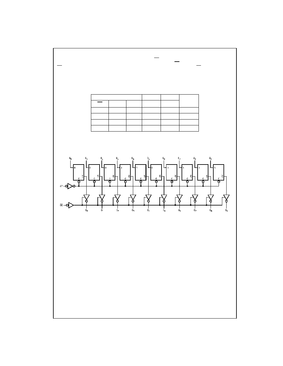
The AC/ACT821 consists of ten D-type edge-triggered flip-
flops. The buffered Clock (CP) and buffered Output Enable
(OE) are common to all flip-flops. The flip-flops will store
the state of their individual D inputs that meet the setup and
hold time requirements on the LOW-to-HIGH CP transition.
With OE LOW the contents of the flip-flops are available at
the outputs. When OE is HIGH the outputs go to the high
impedance state. Operation of the OE input does not affect
the state of the flip-flops.
Function Table
H
=
HIGH Voltage Level
L
=
LOW Voltage Level
Z
=
HIGH Impedance
=
LOW-to-HIGH Clock Transition
Logic Diagram
Please note that this diagram is provided only for the understanding of logic operations and should not be used to estimate propagation delays.
Inputs
Internal
Outputs
Function
OE
CP
D
Q
O
H
L
L
Z
High Z
H
H
H
Z
High Z
L
L
L
L
Load
L
H
H
H
Load

3
www.fairchildsemi.com
74
A
C
82
1
∑
74ACT821
Absolute Maximum Ratings
(Note 1)
Recommended Operating
Conditions
Note 1: Absolute maximum ratings are those values beyond which damage
to the device may occur. The databook specifications should be met, with-
out exception, to ensure that the system design is reliable over its power
supply, temperature, and output/input loading variables. Fairchild does not
recommend operation of FACT
circuits outside databook specifications.
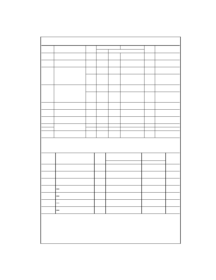
DC Electrical Characteristics for AC
Note 2: All outputs loaded; thresholds on input associated with output under test.
Note 3: Maximum test duration 2.0 ms, one output loaded at a time.
Note 4: I
IN
and I
CC
@ 3.0V are guaranteed to be less than or equal to the respective limit @ 5.5V V
CC
.
Supply Voltage (V
CC
)
-
0.5V to
+
7.0V
DC Input Diode Current (I
IK
)
V
I
=
-
0.5V
-
20 mA
V
I
=
V
CC
+
0.5V
+
20 mA
DC Input Voltage (V
I
)
-
0.5V to V
CC
+
0.5V
DC Output Diode Current (I
OK
)
V
O
=
-
0.5V
-
20 mA
V
O
=
V
CC
+
0.5V
+
20 mA
DC Output Voltage (V
O
)
-
0.5V to V
CC
+
0.5V
DC Output Source
or Sink Current (I
O
)
±
50 mA
DC V
CC
or Ground Current
per Output Pin (I
CC
or I
GND
)
±
50 mA
Storage Temperature (T
STG
)
-
65
∞
C to
+
150
∞
C
Junction Temperature (T
J
)
PDIP
140
∞
C
Supply Voltage (V
CC
)
AC
2.0V to 6.0V
ACT
4.5V to 5.5V
Input Voltage (V
I
)
0V to V
CC
Output Voltage (V
O
)
0V to V
CC
Operating Temperature (T
A
)
-
40
∞
C to
+
85
∞
C
Minimum Input Edge Rate (
V/
t)
AC Devices
V
IN
from 30% to 70% of V
CC
V
CC
@ 3.3V, 4.5V, 5.5V
125 mV/ns
Minimum Input Edge Rate (
V/
t)
ACT Devices
V
IN
from 0.8V to 2.0V
V
CC
@ 4.5V, 5.5V
125 mV/ns
Symbol
Parameter
V
CC
T
A
=
+
25
∞
C
T
A
=
-
40
∞
C to
+
85
∞
C
Units
Conditions
(V)
Typ
Guaranteed Limits
V
IH
Minimum HIGH Level
3.0
1.5
2.1
2.1
V
OUT
=
0.1V
Input Voltage
4.5
2.25
3.15
3.15
V
or V
CC
-
0.1V
5.5
2.75
3.85
3.85
V
IL
Maximum LOW Level
3.0
1.5
0.9
0.9
V
OUT
=
0.1V
Input Voltage
4.5
2.25
1.35
1.35
V
or V
CC
-
0.1V
5.5
2.75
1.65
1.65
V
OH
Minimum HIGH Level
3.0
2.99
2.9
2.9
Output Voltage
4.5
4.49
4.4
4.4
V
I
OUT
=
-
50
µ
A
5.5
5.49
5.4
5.4
V
IN
=
V
IL
or V
IH
3.0
2.56
2.46
I
OH
=
-
12 mA
4.5
3.86
3.76
V
I
OH
=
-
24 mA
5.5
4.86
4.76
I
OH
=
-
24 mA (Note 2)
V
OL
Maximum LOW Level
3.0
0.002
0.1
0.1
Output Voltage
4.5
0.001
0.1
0.1
V
I
OUT
=
50
µ
A
5.5
0.001
0.1
0.1
V
IN
=
V
IL
or V
IH
3.0
0.36
0.44
I
OL
=
12 mA
4.5
0.36
0.44
V
I
OL
=
24 mA
5.5
0.36
0.44
I
OL
=
24 mA (Note 2)
I
IN
(Note 4)
Maximum Input Leakage Current
5.5
±
0.1
±
1.0
µ
A
V
I
=
V
CC
, GND
I
OZ
Maximum 3-STATE Current
V
I
(OE)
=
V
IL
, V
IH
5.5
±
0.5
±
5.0
µ
A
V
I
=
V
CC
, GND
V
O
=
V
CC
, GND
I
OLD
Minimum Dynamic
5.5
75
mA
V
OLD
=
1.65V Max
I
OHD
Output Current (Note 3)
5.5
-
75
mA
V
OHD
=
3.85V Min
I
CC
(Note 4)
Maximum Quiescent Supply Current
5.5
8.0
80.0
µ
A
V
IN
=
V
CC
or GND
www.fairchildsemi.com
4
74AC821
∑
74ACT821
DC Electrical Characteristics for ACT
Note 5: All outputs loaded; thresholds on input associated with output under test.
Note 6: Maximum test duration 2.0 ms, one output loaded at a time.
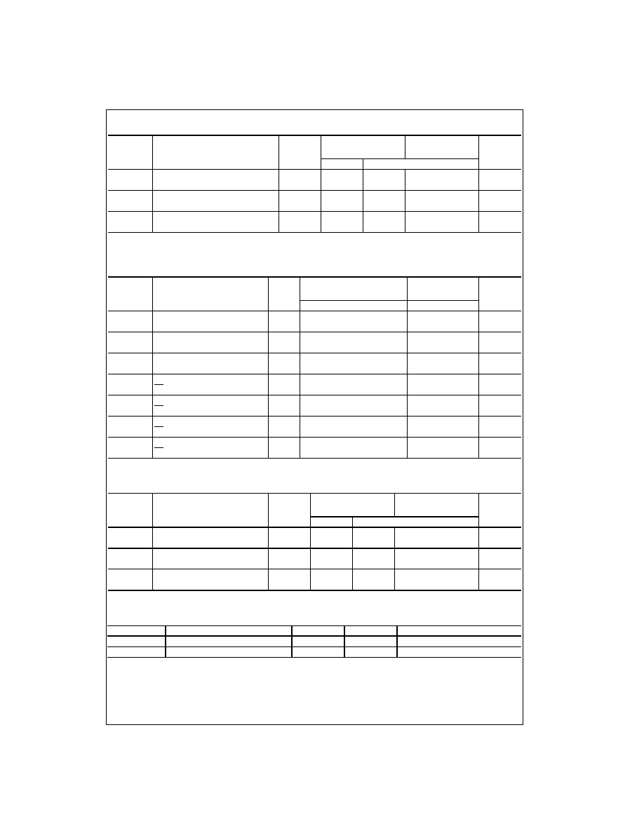
AC Electrical Characteristics for AC
Note 7: Voltage Range 3.3 is 3.3V
±
0.3V
Voltage Range 5.0 is 5.0V
±
0.5V
Symbol
Parameter
V
CC
T
A
=
+
25
∞
C
T
A
=
-
40
∞
C to
+
85
∞
C
Units
Conditions
(V)
Typ
Guaranteed Limits
V
IH
Minimum HIGH Level
4.5
1.5
2.0
2.0
V
V
OUT
=
0.1V
Input Voltage
5.5
1.5
2.0
2.0
or V
CC
-
0.1V
V
IL
Maximum LOW Level
4.5
1.5
0.8
0.8
V
V
OUT
=
0.1V
Input Voltage
5.5
1.5
0.8
0.8
or V
CC
-
0.1V
V
OH
Minimum HIGH Level
4.5
4.49
4.4
4.4
V
I
OUT
=
-
50
µ
A
Output Voltage
5.5
5.49
5.4
5.4
V
IN
=
V
IL
or V
IH
4.5
3.86
3.76
V
I
OH
=
-
24 mA
5.5
4.86
4.76
I
OH
=
-
24 mA (Note 5)
V
OL
Maximum LOW Level
4.5
0.001
0.1
0.1
V
I
OUT
=
50
µ
A
Output Voltage
5.5
0.001
0.1
0.1
V
IN
=
V
IL
or V
IH
4.5
0.36
0.44
V
I
OL
=
24 mA
5.5
0.36
0.44
I
OL
=
24 mA (Note 5)
I
IN
Maximum Input
5.5
±
0.1
±
1.0
µ
A
V
I
=
V
CC
, GND
(Note 4)
Leakage Current
I
OZ
Maximum 3-STATE
5.5
±
0.5
±
5.0
µ
A
V
I
=
V
IL
, V
IH
Current
V
O
=
V
CC
, GND
I
CCT
Maximum
5.5
0.6
1.5
mA
V
I
=
V
CC
-
2.1V
I
CC
/Input
I
OLD
Minimum Dynamic
5.5
75
mA
V
OLD
=
1.65V Max
I
OHD
Output Current (Note 6)
5.5
-
75
mA
V
OHD
=
3.85V Min
I
CC
Maximum Quiescent
5.5
8.0
80.0
µ
A
V
IN
=
V
CC
Supply Current
or GND
V
CC
T
A
=
+
25
∞
C
T
A
=
-
40
∞
C to
+
85
∞
C
Symbol
Parameter
(V)
C
L
=
50 pF
C
L
=
50 pF
Units
(Note 7)
Min
Typ
Max
Min
Max
f
MAX
Maximum Clock
3.3
110
145
100
MHz
Frequency
5.0
120
160
110
t
PLH
Propagation Delay
3.3
3.0
8.0
13.0
3.0
15.0
ns
CP to O
n
5.0
2.0
6.0
9.5
2.0
10.5
t
PHL
Propagation Delay
3.3
3.0
8.0
13.0
3.0
15.0
ns
CP to O
n
5.0
2.0
5.5
9.5
2.0
10.5
t
PZH
Output Enable Time
3.3
2.5
6.0
11.0
2.5
12.0
ns
OE to O
n
5.0
1.5
4.5
8.0
1.5
9.0
t
PZL
Output Enable Time
3.3
2.5
6.5
11.0
2.5
12.0
ns
OE to O
n
5.0
1.5
5.0
8.0
1.5
9.0
t
PHZ
Output Disable Time
3.3
2.5
6.5
10.5
2.5
11.0
ns
OE to O
n
5.0
1.5
5.0
8.0
1.5
8.5
t
PLZ
Output Disable Time
3.3
2.5
6.0
10.5
2.5
11.0
ns
OE to O
n
5.0
1.5
4.5
8.0
1.5
8.5
5
www.fairchildsemi.com
74
A
C
82
1
∑
74ACT821
AC Operating Requirements for AC
Note 8: Voltage Range 3.3 is 3.3V
±
0.3V
Voltage Range 5.0 is 5.0V
±
0.5V
AC Electrical Characteristics for ACT
Note 9: Voltage Range 5.0 is 5.0V
±
0.5V
AC Operating Requirements for ACT
Note 10: Voltage Range 5.0 is 5.0V
±
0.5V
Capacitance
V
CC
T
A
=
+
25
∞
C
T
A
=
-
40
∞
C to
+
85
∞
C
Symbol
Parameter
(V)
C
L
=
50 pF
C
L
=
50 pF
Units
(Note 8)
Typ
Guaranteed Minimum
t
S
Setup Time, HIGH or LOW
3.3
-
1.0
1.5
1.5
ns
D
n
to CP
5.0
-
1.0
1.5
1.5
t
H
Hold Time, HIGH or LOW
3.3
-
1.0
3.5
4.0
ns
D
n
to CP
5.0
-
1.0
3.5
4.0
t
W
CP Pulse Width
3.3
3.5
5.0
5.5
ns
HIGH or LOW
5.0
2.5
4.0
4.0
V
CC
T
A
=
+
25
∞
C
T
A
=
-
40
∞
C to
+
85
∞
C
Symbol
Parameter
(V)
C
L
=
50 pF
C
L
=
50 pF
Units
(Note 9)
Min
Typ
Max
Min
Max
f
MAX
Maximum Clock
5.0
120
150
110
MHz
Frequency
t
PLH
Propagation Delay
5.0
2.0
6.0
9.5
1.5
10.5
ns
CP to O
n
t
PHL
Propagation Delay
5.0
2.5
6.0
9.5
2.0
10.5
ns
CP to O
n
t
PZH
Output Enable Time
5.0
2.5
7.0
10.5
2.0
11.5
ns
OE to O
n
t
PZL
Output Enable Time
5.0
2.5
7.0
10.5
2.0
12.0
ns
OE to O
n
t
PHZ
Output Disable Time
5.0
1.5
7.5
12.0
1.0
13.0
ns
OE to O
n
t
PLZ
Output Disable Time
5.0
1.5
7.0
10.5
1.0
11.5
ns
OE to O
n
V
CC
T
A
=
+
25
∞
C
T
A
=
-
40
∞
C to
+
85
∞
C
Symbol
Parameter
(V)
C
L
=
50 pF
C
L
=
50 pF
Units
(Note 10)
Typ
Guaranteed Minimum
t
S
Setup Time, HIGH or LOW
5.0
2.5
2.0
2.5
ns
D
n
to CP
t
H
Hold Time, HIGH or LOW
5.0
-
0.5
2.0
2.5
ns
D
n
to CP
t
W
CP Pulse Width
5.0
3.0
4.5
5.5
ns
HIGH or LOW
Symbol
Parameter
Typ
Units
Conditions
C
IN
Input Capacitance
4.5
pF
V
CC
=
OPEN
C
PD
Power Dissipation Capacitance
35.0
pF
V
CC
=
5.0V
www.fairchildsemi.com
6
74AC821
∑
74ACT821
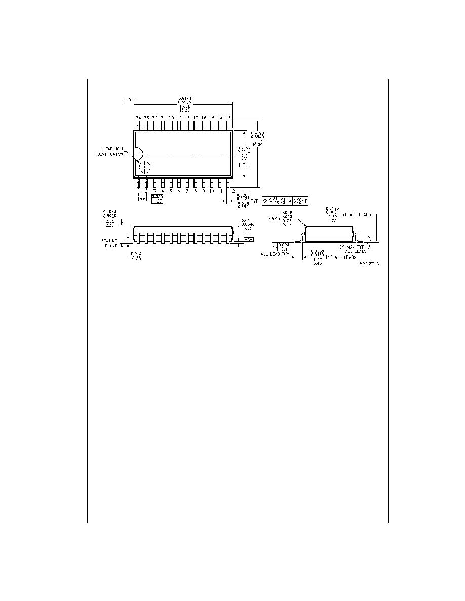
Physical Dimensions
inches (millimeters) unless otherwise noted
24-Lead Small Outline Integrated Circuit (SOIC), JEDEC MS-013, 0.300 Wide
Package Number M24B

7
www.fairchildsemi.com
74
A
C
82
1
∑
74ACT821
Physical Dimensions
inches (millimeters) unless otherwise noted (Continued)
24-Lead Thin Shrink Small Outline Package (TSSOP), JEDEC MO-153, 4.4mm Wide
Package Number MTC24
www.fairchildsemi.com
8
74AC821
∑
74
A
C
T8
21 10-
Bit
D-
T
ype F
l
i
p
-Fl
op wi
th
3-
S
T
A
T
E
O
u
t
puts
Physical Dimensions
inches (millimeters) unless otherwise noted (Continued)
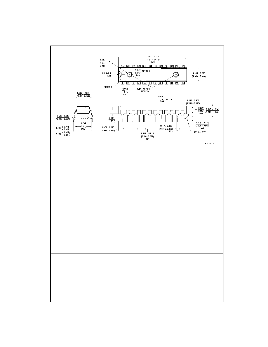
24-Lead Plastic Dual-In-Line Package (PDIP), JEDEC MS-001, 0.300 Wide
Package Number N24C
Fairchild does not assume any responsibility for use of any circuitry described, no circuit patent licenses are implied and
Fairchild reserves the right at any time without notice to change said circuitry and specifications.
LIFE SUPPORT POLICY
FAIRCHILD'S PRODUCTS ARE NOT AUTHORIZED FOR USE AS CRITICAL COMPONENTS IN LIFE SUPPORT
DEVICES OR SYSTEMS WITHOUT THE EXPRESS WRITTEN APPROVAL OF THE PRESIDENT OF FAIRCHILD
SEMICONDUCTOR CORPORATION. As used herein:
1. Life support devices or systems are devices or systems
which, (a) are intended for surgical implant into the
body, or (b) support or sustain life, and (c) whose failure
to perform when properly used in accordance with
instructions for use provided in the labeling, can be rea-
sonably expected to result in a significant injury to the
user.
2. A critical component in any component of a life support
device or system whose failure to perform can be rea-
sonably expected to cause the failure of the life support
device or system, or to affect its safety or effectiveness.
www.fairchildsemi.com