Äîêóìåíòàöèÿ è îïèñàíèÿ www.docs.chipfind.ru
www.fairchildsemi.com
REV. 1.0.0 1/9/01
Features
· Low Voltage CMOS or PECL reference input
· Up to 175 MHz of output frequency
· Nine configurable outputs
· Output enable pin
· 250 pS of output to output skew
· 300 pS of Cycle to Cycle Jitter
· V
DD
Range of 3.3V ±0.2V
· Commercial temperature range
· Available in 32 pin TQFP
Description
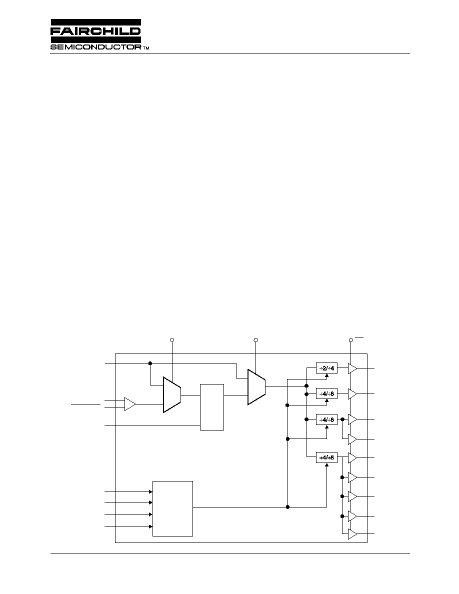
FMS7951 is a high speed, zero delay, low skew clock driver. It
uses phase locked loop technology to generate frequencies up
to 175 MHz.
It has four banks of configurable outputs. By externally con-
necting one of the outputs to FBIN, the internal PLL will
lock in both phase and frequency to the incoming clock. Any
changes to the input clock will be tracked by the outputs.
Depending on the selected output for feedback connection,
the output frequencies will be as 1X, 2X or 4X of the input.
REF_SEL allows selection between PECL input or TCLK a
CMOS clock driven input. Connecting PLL_EN LOW and
REF_SEL HIGH will by pass the Phase locked loop. In this
mode, FMS7951 will be in clock buffer mode where any
clock applied to TCLK will be divided down to the four out-
put banks. This is ideal for system diagnostic test. When
PLL_EN is HIGH, the PLL is enabled, and any clock applied
to TCLK will be locked in both phase and frequency to
FBIN. PECL_CLK is activated when REF_SEL is high.
FMS7951 operates at 3.3 Volts and is available in 32 pin LQFP.
FMS7951
Zero Delay Clock Multiplier
Block Diagram
MUX
MUX
DIV_SEL A
TCLK
FBIN
PECL_CLK
PECL_CLK
DIV_SEL B
DIV_SEL C
DIV_SEL D
QA
QB
QC0
QC1
QD0
QD1
QD2
QD3
QD4
OE
PLL
Control
Logic
PLL_EN
REF_SEL
PRODUCT SPECIFICATION
FMS7951
2
REV. 1.0.0 1/9/01
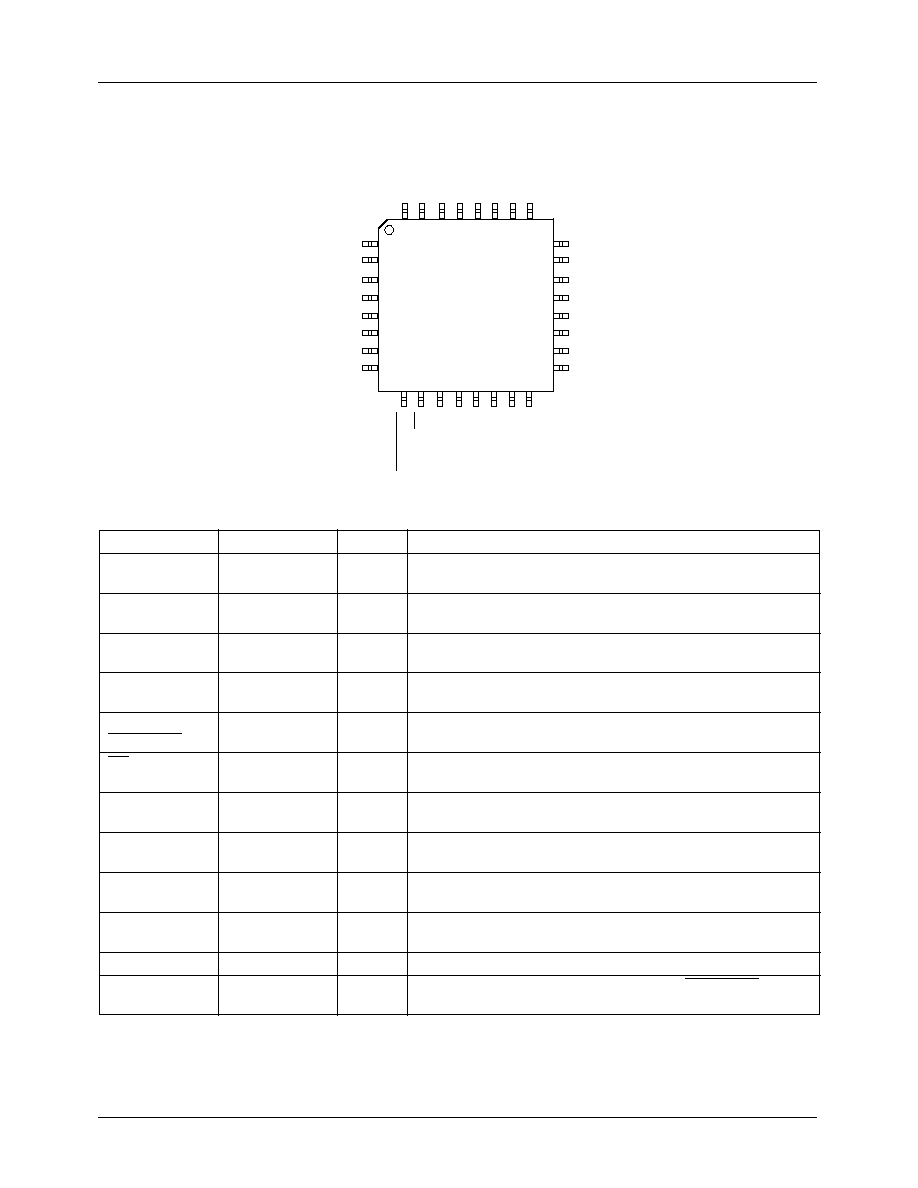
Pin Assignments
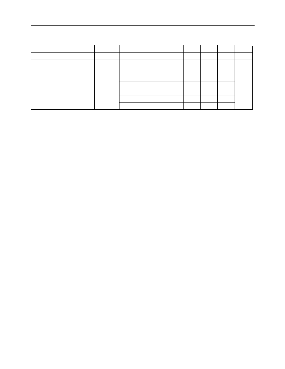
Pin Description
Pin Name
Pin #
Pin Type
Description
VDDCOR
1
PWR
Power Connection.
Power supply for core logic and PLL
circuitry. Connect to 3.3 Volts nominal.
FBIN
2
IN
Feedback In.
PLL feedback input. The user connects it to one of
the outputs.
DIV_SEL(A:D)
3, 4, 5, 6
IN
Divider Select:
It divides the clock to a desirable value. See
table 2. No internal pull up or pull down.
GNDCOR
7
PWR
Ground Connection.
Ground for core logic and PLL circuitry.
Connect to the common system ground plane.
PECL_CLK/
PECL_CLK
8, 9
IN
PECL Clock Input:
These are differential PECL inputs when
REF_SEL is Low, they are activated.
OE
10
IN
Output Enable.
When high, all outputs are in high impedance.
Normal operation when asserted low.
VDDOUT
11, 15, 19, 23, 27
PWR
Power Connection.
Power supply for all the output buffers.
Connect to 3.3 Volts nominal.
Q
A
; Q
B
; Q
C
(0:1);
Q
D
(0:4)
12, 14, 16, 18, 20,
22, 24, 26, 28
OUT
Clock Outputs.
These outputs are multiple of the input.
GNDOUT
13, 17, 21, 25, 29
PWR
Ground Connection.
Ground for all the outputs. Connect to
common system ground plane.
TCLK
30
IN
Test Clock.
When PLL-EN is low, all outputs are buffer copy of
TCLK.
PLL_EN
31
IN
PLL Enable.
When low, PLL is by passed.
REF_SEL
32
IN
Reference Select.
When low, PECL_CLK/PECL_CLK is used
for input. When high, TCLK is used for input.
25
26
27
28
29
30
31
32
16
15
14
13
12
11
10
9
24
23
22
21
20
19
18
17
1
2
3
4
5
6
7
8
GNDOUT
GNDOUT
TCLK
REF_SEL
PLL_EN
QB
QA
VDDOUT
QC0
QD0
VDDOUT
GNDOUT
QD1
VDDOUT
GNDOUT
QC1
VDDCOR
32-PIN
LQFP
DIV_SEL C
DIV_SEL D
PECL_CLK
GNDCOR
FBIN
DIV_SEL B
DIV_SEL A
QD2
QD4
VDDOUT
PECL_CLK
OE
VDDOUT
GNDOUT
QD3
FMS7951
PRODUCT SPECIFICATION
REV. 1.0.0 1/9/01
3
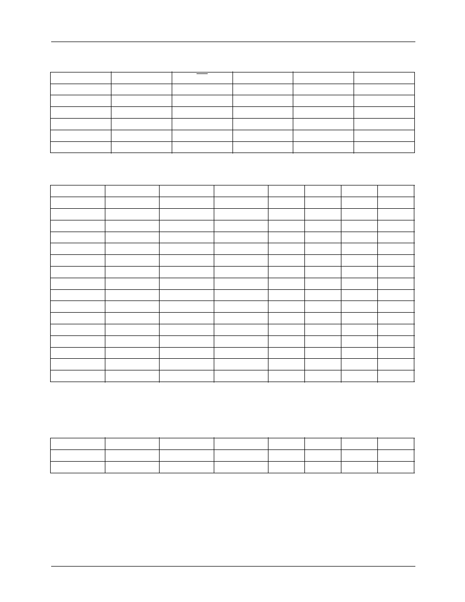
Note:
1. Reference input could be either PECL_CLK or TCLK input.
2. FBIN is tied to QD output for table
Table 1. Functionality
REF_SEL
PLL_EN
OE
PLL
All Outputs
Input
0
0
1
By Pass
Hi-Z
PECL_CLK
0
0
0
By Pass
Running
PECL_CLK
0
1
0
Enabled
Running
PECL_CLK
1
0
1
By Pass
Hi-Z
TCLK
1
0
0
By Pass
Running
TCLK
1
1
0
Enabled
Running
TCLK
Table 2. Input Versus Output Frequency
DIV_SELA
DIV_SELB
DIV_SELC
DIV_SELD
QA
QB
QC
QD
0
0
0
0
2XREF
REF
REF
REF
0
0
0
1
4XREF
2XREF
2XREF
REF
0
0
1
0
2XREF
REF
1/2REF
REF
0
0
1
1
4XREF
2XREF
REF
REF
0
1
0
0
2XREF
1/2REF
REF
REF
0
1
0
1
4XREF
REF
2XREF
REF
0
1
1
0
2XREF
1/2REF
1/2REF
REF
0
1
1
1
4XREF
REF
REF
REF
1
0
0
0
REF
REF
REF
REF
1
0
0
1
2XREF
2XREF
2XREF
REF
1
0
1
0
REF
REF
1/2REF
REF
1
0
1
1
2XREF
2XREF
REF
REF
1
1
0
0
REF
1/2REF
REF
REF
1
1
0
1
2XREF
REF
2XREF
REF
1
1
1
0
REF
1/2REF
1/2REF
REF
1
1
1
1
2XREF
REF
REF
REF
Table 3. Divide Select Functionality
DIV_SEL A
DIV_SEL B
DIV_SEL D
DIV_SEL D
QA
QB
QC
QD
0
0
0
0
÷
2
÷
4
÷
4
÷
4
1
1
1
1
÷
4
÷
8
÷
8
÷
8
PRODUCT SPECIFICATION
FMS7951
4
REV. 1.0.0 1/9/01
Absolute Maximum Ratings
Stresses greater than those listed in the table may cause permanent damage to the device. These represent a stress rating only.
Operation of the device at these or any other conditions above those specified in the operating sections of this specification is
not implied. Maximum conditions for extended periods may effect reliability.
DC Electrical Characteristics
T
A
= 0 to 70°C; Supply Voltage 3.3 V ±0.2V (unless otherwise stated)
Note:
1. Guaranteed by design, not subject to 100% production testing.
AC Electrical Characteristics
T
A
= 0 to 70°C; Supply Voltage V
DD
= 3.3V ±0.2V, C
L
= 10 pF (unless otherwise stated)
Symbol
Parameter
Ratings
Units
V
DD
, V
IN
Voltage on any pin with respect to ground
-0.5 to 7.0
V
T
STG
Storage Temperature
-65 to 150
°C
T
B
Ambient Temperature
-55 to 125
°C
T
A
Operating Temperature
0 to 70
°C
Parameter
Symbol
Conditions
Min.
Typ.
Max.
Units
Input Low Voltage
V
IL
TCLK; control pins
0.8
V
Input High Voltage
V
IH
TCLK; control pins
2.0
3.6
V
Input Low Current
I
IL
V
IN
= 0
-10
10
µA
Input High Current
I
IH
V
IN
= V
DD
-30
30
µA
Peak to Peak Input
Voltage
V
PP
PECL_CLK/PCL_CLK
0.3
1.0
V
Common Mode Range
V
CMR
V
DD
-2.0
V
DD
-0.6
mV
Output Low Voltage
V
OL
I
OL
= 40 mA
0.5
V
Output High Voltage
V
OH
I
OH
= 40mA
2.2
V
Input Capacitance
(1)
C
IN
7.0
pF
Supply Current
I
DD
Outputs loaded
TBD
150
mA
Clock Stabilization
(1)
T
STAB
From V
DD
= 3.3V to 1% Target
10
mS
Parameter
Symbol
Conditions
Min.
Typ.
Max.
Units
Input Frequency
F
IN
Feedback Divide = 2
10
175
MHz
Feedback Divide = 4
10
85
Feedback Divide = 8
10
42
TCLK Input Rise/Fall Time
(1)
T
R_IN
/T
F_IN
3.0
ns
TCLK Input Duty Cycle
(1)
D
T_IN
25
75
%
Output Frequency Range
F
OUT
Q
A
; DIV_SEL A = 0V
175
MHz
Q
B
, Q
C
& Q
D
;
DIV_SEL B, C, D = 0V
88
MHz
Output to Output Skew
T
SK1
V
TH
= V
DD
/2; DIV_SEL A = 0
750
pS
V
TH
= V
DD
/2; DIV_SEL A = 1
-300
300
Input to FBIN Delay
T
SK2
TCLK
50
400
pS
PECL_CLK
-950
-600
FMS7951
PRODUCT SPECIFICATION
REV. 1.0.0 1/9/01
5
Note:
1. Guaranteed by design, not subject to 100% production testing.
Rise Time
(1)
T
R
0.8 to 2.0V
0.10
1.0
nS
Fall Time
(1)
T
F
2.0 to 0.8V
0.10
1.0
nS
Duty Cycle
(1)
D
T
V
TH
= V
DD
/2
45
55
%
Jitter (Cycle-Cycle)
T
JIT
QA: DIV_SEL A = 0
450
pS
QA: DIV_SEL A = 1
200
QB Output
200
QC(0:1) Outputs
300
QD(0:4) Outputs
375
Parameter
Symbol
Conditions
Min.
Typ.
Max.
Units
AC Electrical Characteristics
(Cont.)
T
A
= 0 to 70°C; Supply Voltage V
DD
= 3.3V ±0.2V, C
L
= 10 pF (unless otherwise stated)