 | ÐлекÑÑоннÑй компоненÑ: FOD0708R2 | СкаÑаÑÑ:  PDF PDF  ZIP ZIP |
Äîêóìåíòàöèÿ è îïèñàíèÿ www.docs.chipfind.ru
January 2006
FOD0708 Single Channel CMOS Optocoupler FOD0738 Dual Channel CMOS Optocoupler
©2005 Fairchild Semiconductor Corporation
1
www.fairchildsemi.com
FOD0708 Single Channel CMOS Optocoupler Rev. 1.0.6
FOD0708 Single Channel CMOS Optocoupler
FOD0738 Dual Channel CMOS Optocoupler
Features
+5 V CMOS compatibility
15 ns typical pulse width distortion
30 ns max. pulse width distortion
40 ns max. propagation delay skew
High speed: 15 MBd
60 ns max. propagation delay
10 kV/µs minimum common mode rejection
40°C to 100°C temperature range
UL approved (file #E90700)
Applications
Line receivers
Pulse transformer replacement
Output interface to CMOS-LSTTL-TTL
Wide bandwidth analog coupling
General Description
The FOD0708 and FOD0738 optocouplers consist of an
AlGaAs LED optically coupled to a high speed trans-
impedance amplifier and voltage comparator. These
optocouplers utilize the latest CMOS IC technology to
achieve outstanding performance with very low power
consumption. The devices are housed in a compact
8-pin SOIC package for optimum mounting density.
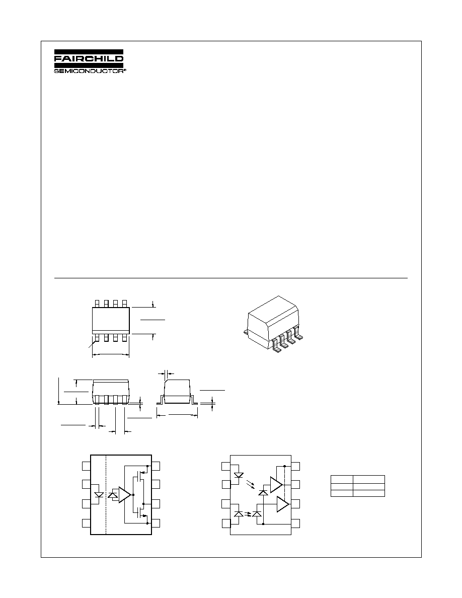
Package Dimensions
Lead Coplanarity : 0.004 (0.10) MAX
0.202 (5.13)
Pin 1
0.019 (0.48)
0.182 (4.63)
0.021 (0.53)
0.011 (0.28)
0.050 (1.27)
TYP
0.244 (6.19)
0.224 (5.69)
0.143 (3.63)
0.123 (3.13)
0.008 (0.20)
0.003 (0.08)
0.010 (0.25)
0.006 (0.16)
SEATING P
LANE
0.164 (4.16)
0.144 (3.66)
Note: A 0.1
µ
F bypass capacitor
must be connected between
pins 5 and 8.
8
7
6
1
3
5
2
4
NC
ANODE
CATHODE
NC
V
DD
V
O
GND
LED
OFF
ON
TRUTH TABLE
FOD0708
FOD0738
NC
V
O
, OUTPUT
L
H
8
7
6
1
3
5
2
4
ANODE 1
CATHODE 1
CATHODE 2
ANODE 2
V
DD
V
O
2
GND
V
O
1
2
www.fairchildsemi.com
FOD0708/FOD0738 Rev. 1.0.6
FOD0708 Single Channel CMOS Optocoupler FOD0738 Dual Channel CMOS Optocoupler
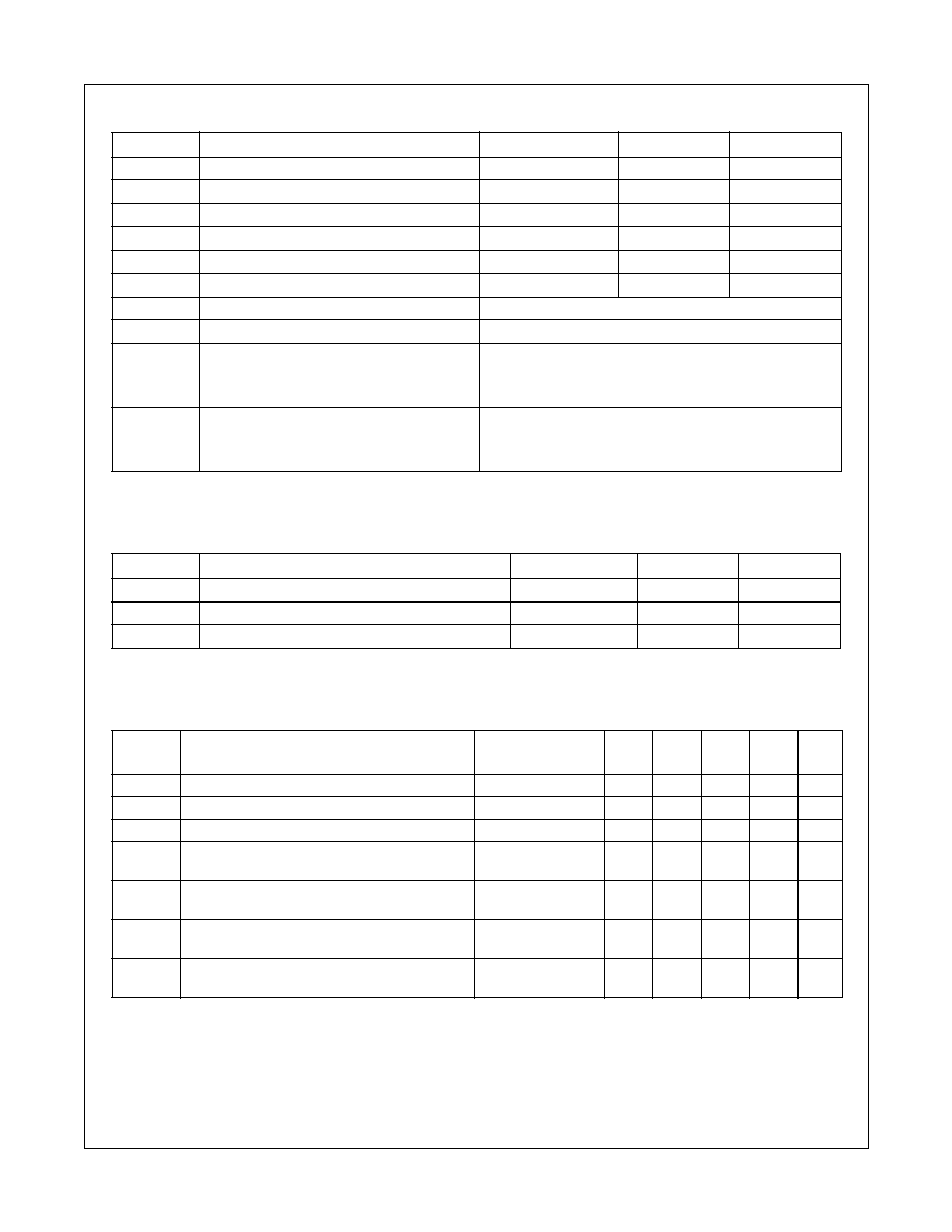
Absolute Maximum Ratings
T
A
= 25°C unless otherwise noted
Recommended Operating Conditions
Electrical Characteristics
(T
A
= 40°C to +100°C) and 4.5 V
V
DD
5.5 V
*All typicals at T
A
= 25°C and V
DD
= 5V unless otherwise noted.
Symbol Parameter
Min.
Max.
Units
T
S
Storage Temperature
40
+125
°C
T
A
Ambient Operating Temperature
40
+100
°C
V
DD
Supply Voltages
0
6
Volts
V
O
Output Voltage
0.5
V
DD
+ 0.5
Volts
I
O
Average Output Current
2
mA
I
F
Average Forward Input Current
20
mA
Lead Solder Temperature
260°C for 10 sec., 1.6 mm below seating plane
Solder Reflow Temperature Profile
See Solder Reflow Temperature Profile Section
LED Power Dissipation
Single Channel
Dual Channel
40 mW (derate above 95°C, 1.4 mW/°C)
40 mW per channel (derate above 90°C, 1.2 mW/°C)
Detector Power Dissipation
Single Channel
Dual Channel
85 mW (derate above 75°C, 1.8 mW/°C)
65 mW per channel (derate above 90°C, 2.0 mW/°C)
Symbol Parameter
Min.
Max.
Units
T
A
Ambient Operating Temperature
40
+100
°C
V
DD
Supply Voltages
4.5
5.5
Volts
I
F
Input Current (ON)
10
16
mA
Symbol Parameter
Test
Conditions Min.
Typ.*
Max.
Units
Fig.
V
F
Input Forward Voltage
I
F
= 12 mA
1.3
1.45
1.8
V
9
BV
R
Input Reverse Breakdown Voltage
I
R
= 10 µA
5
V
V
OH
Logic High Output Voltage
I
F
= 0, I
O
= 20 µA
4.0
5.0
V
V
OL
Logic Low Output Voltage
I
F
= 12 mA,
I
O
= 20 µA
0.01 0.1 V
I
TH
Input Threshold Current
(FOD0708)
(FOD0738)
I
OL
= 20 µA
4.0
4.4
8.2
8.2
mA 1,5
I
DDL
Logic Low Output Supply Current
(FOD0708)
(FOD0738)
I
F
= 12 mA
3.4
6.9
14.0
18.0
mA 3,7
I
DDH
Logic High Output Supply Current (FOD0708)
(FOD0738)
I
F
= 0
3.7
7.5
11.0
15.0
mA 4,8
3
www.fairchildsemi.com
FOD0708/FOD0738 Rev. 1.0.6
FOD0708 Single Channel CMOS Optocoupler FOD0738 Dual Channel CMOS Optocoupler
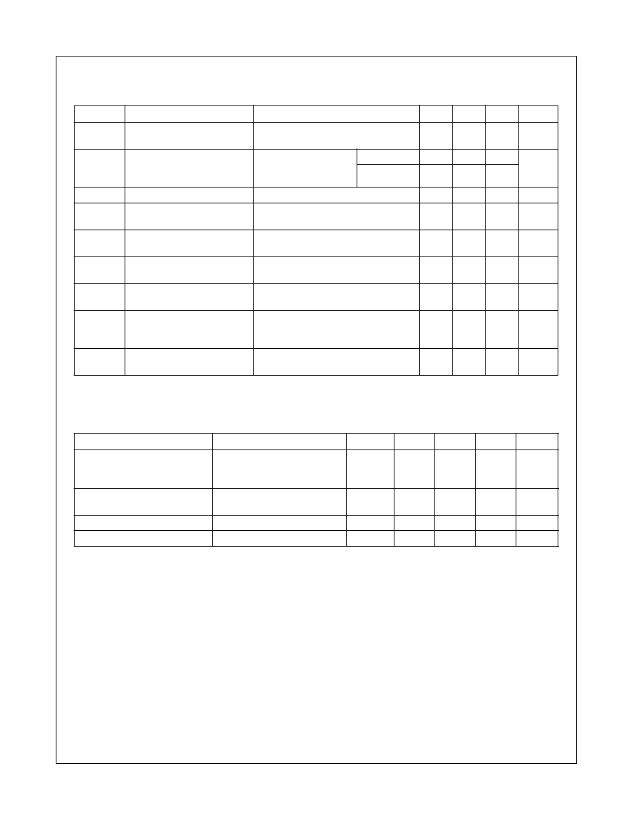
Switching Characteristics
Over recommended temperature (T
A
= 40°C to +100°C) and
4.5 V
V
DD
5.5 V. All typical specifications are at T
A
= 25°C, V
DD
= +5 V.
*All typicals at T
A
= 25°C and V
DD
= 5V unless otherwise noted.
Isolation Characteristics
(T
A
= -40°C to +100°C Unless otherwise specified.)
** All typical values are at V
CC
= 5 V, T
A
= 25°C
Notes:
1.
Propagation delay time, high to low (t
PHL
), is measured from the 50% level on the rising edge of the input pulse to the 2.5V level
of the falling edge of the output voltage signal. Propagation delay time, low to high (t
PLH
), is measured from the 50% level on the
falling edge of the input pulse to the 2.5V level of the rising edge of the output voltage signal.
2.
Pulse width distoration is defined as the absolute difference between the high to low and low to high propagation delay times,
| t
PHL
t
PLH
|.
3.
Propagation delay skew, t
PSK
, is defined as the worst case difference in t
PHL
or t
PLH
between units within the recommended
operating range of the device.
4.
CM
H
The maximum tolerated rate of rise of the common mode voltage to ensure the output will remain in the high state,
(i,e., V
OUT
> 2.0V) Measured in kilovolts per microsecond (kV/µs).
5.
CM
L
The maximum tolerated rate of fall of the common mode voltage to ensure the output will remain in the low state,
(i,e., V
OUT
< 0.8V). Measured in kilovolts per microsecond (kV/µs).
6.
Isolation voltage, V
ISO
, is an internal device dielectric breakdown rating. For this test, pins 1,2,3,4 are common, and pins 5,6,7,8
are common.
Symbol Parameter
Test
Conditions Min.
Typ.*
Max.
Units
t
PHL
Propagation Delay Time to
Logic Low Output
I
F
= 12 mA, C
L
= 15 pF
CMOS Signal Levels, note 1, fig. 10
20 60 ns
t
PLH
Propagation Delay Time to
Logic High Output
I
F
= 12 mA, C
L
= 15 pF
CMOS Signal Levels,
note 1, fig. 10
FOD0708
13 60 ns
FOD0738
11
60
PW Pulse
Width
100
ns
| PWD |
Pulse Width Distortion
I
F
= 12 mA, C
L
= 15 pF
CMOS Signal Levels, note 2
0 30
ns
t
PSK
Propagation Delay Skew
I
F
= 12 mA, C
L
= 15 pF
CMOS Signal Levels, note 3
40 ns
t
R
Output Rise Time (10%90%) I
F
= 12 mA, C
L
= 15 pF
CMOS Signal Levels
12 ns
t
F
Output Fall Time (90%10%) I
F
= 12 mA, C
L
= 15 pF
CMOS Signal Levels
8 ns
| CM
H
|
Common Mode Transient
Immunity at Logic High
Output
V
CM
= 1000 V, T
A
= 25°C, I
F
= 0 mA,
note 4, fig. 11
25
50
kV/µs
| CM
L
|
Common Mode Transient
Immunity at Logic Low Output
V
CM
= 1000 V, T
A
= 25°C, I
F
= 12 mA,
note 5, fig. 11
25 50
kV/µs
Characteristics
Test Conditions Symbol
Min
Typ.**
Max
Unit
Input-Output Insulation
Leakage Current
(Relative humidity = 45%)
(T
A
= 25°C, t = 5 s)
(V
I-O
= 3000 VDC) (Note 6)
I
I-O
1.0
µA
Withstand Insulation
Test Voltage
(I
I-O
10 µA, R
H
< 50%,
T
A
= 25°C) (t = 1 min.) (Note 6)
V
ISO
2500
V
RMS
Resistance (Input to Output)
(V
I-O
= 500 V) (Note 6)
R
I-O
10
12
Capacitance (Input to Output)
(f = 1 MHz) (Note 6)
C
I-O
0.6
pF
4
www.fairchildsemi.com
FOD0708/FOD0738 Rev. 1.0.6
FOD0708 Single Channel CMOS Optocoupler FOD0738 Dual Channel CMOS Optocoupler
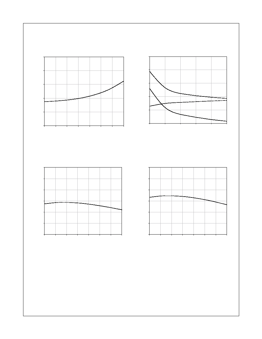
Typical Characteristics
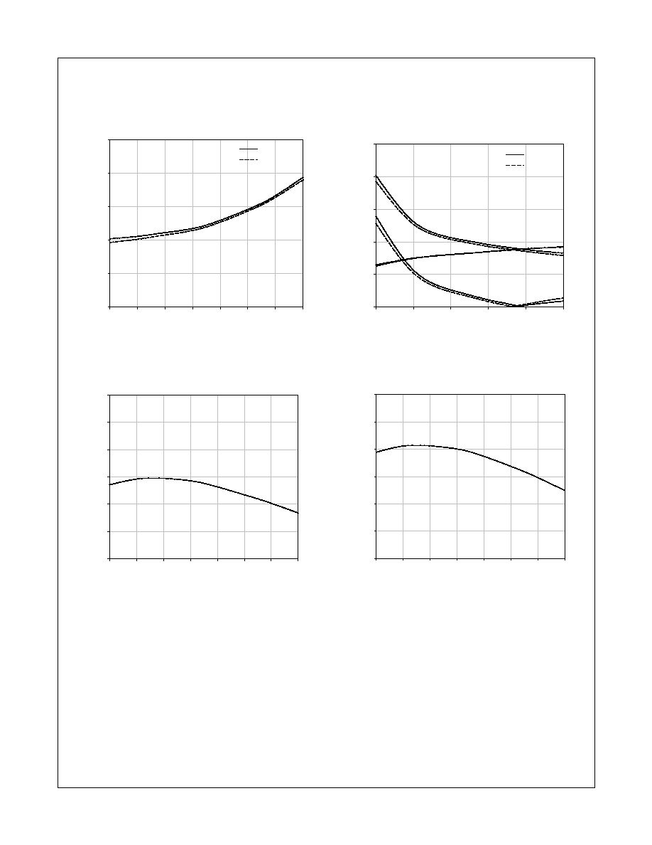
Typical Switching Speed vs Pulse Input Current
I
F
- Pulse Input Current (mA)
5
7
9
11
13
15
t
P
-P
r
o
pag
at
i
o
n
D
el
a
y
(n
s)
0
20
40
60
80
100
V
DD
= 5V
T
A
= 25
o
C
t
PHL
t
PLH
PWD
Typical Logic High Output Supply Current
vs Ambient Temperature
T
A
- Ambient Temperature (
o
C)
-40
-20
0
20
40
60
80
100
I
DD
H
-L
o
g
i
c
H
i
g
h
O
u
tp
ut
Su
ppl
y
C
u
r
r
e
n
t
(
m
A)
2.0
2.5
3.0
3.5
4.0
4.5
5.0
V
DD
= 5V
Typical Logic Low Output Supply Current
vs Ambient Temperature
T
A
- Ambient Temperature (
o
C)
-40
-20
0
20
40
60
80
100
I
DD
L
-L
o
g
i
c
Lo
w
O
ut
p
u
t
S
u
pp
l
y
Cu
rr
en
t
(
mA)
2.0
2.5
3.0
3.5
4.0
4.5
5.0
V
DD
= 5V
I
F
= 12mA
Figure 1. FOD0708
Figure 3. FOD0708
Figure 4. FOD0708
Figure 2. FOD0708
Typical Input Threshold Current
vs Ambient Temperature
T
A
- Ambient Temperature (
o
C)
-40
-20
0
20
40
60
80
100
I
TH
-I
npu
t
T
hresho
l
d
C
u
rrent
(
m
A
)
2
3
4
5
6
7
V
DD
= 5V
I
OL
= 20
µ
A
5
www.fairchildsemi.com
FOD0708/FOD0738 Rev. 1.0.6
FOD0708 Single Channel CMOS Optocoupler FOD0738 Dual Channel CMOS Optocoupler
Typical Characteristics
(Continued)
Typical Logic High Output Supply Current
vs Ambient Temperature
T
A
- Ambient Temperature (
o
C)
-40
-20
0
20
40
60
80
100
I
DD
H
-L
o
g
i
c
H
i
g
h
O
u
tp
ut
Su
ppl
y
C
u
r
r
e
n
t
(
m
A)
5.5
6.0
6.5
7.0
7.5
8.0
8.5
V
DD
= 5V
Typical Logic Low Output Supply Current
vs Ambient Temperature
T
A
- Ambient Temperature (
o
C)
-40
-20
0
20
40
60
80
100
I
DD
L
-L
o
g
i
c
Lo
w
O
ut
p
u
t
S
u
pp
l
y
Cu
rr
en
t
(
mA)
5.5
6.0
6.5
7.0
7.5
8.0
8.5
V
DD
= 5V
I
F
= 12mA
Typical Input Threshold Current
vs Ambient Temperature
T
A
- Ambient Temperature (
o
C)
-40
-20
0
20
40
60
80
100
I
TH
-I
npu
t
T
hresho
l
d
C
u
rrent
(
m
A
)
2
3
4
5
6
7
V
DD
= 5V
I
OL
= 20
µ
A
Channel 1
Channel 2
Typical Switching Speed vs Pulse Input Current
I
F
- Pulse Input Current (mA)
5
7
9
11
13
15
t
P
-P
r
o
pag
at
i
o
n
D
el
a
y
(n
s)
0
20
40
60
80
100
V
DD
= 5V
T
A
= 25
o
C
t
PHL
t
PLH
PWD
Channel 1
Channel 2
Figure 8. FOD0738
Figure 5. FOD0738
Figure 6. FOD0738
Figure 7. FOD0738
6
www.fairchildsemi.com
FOD0708/FOD0738 Rev. 1.0.6
FOD0708 Single Channel CMOS Optocoupler FOD0738 Dual Channel CMOS Optocoupler
Typical Characteristics
(Continued)
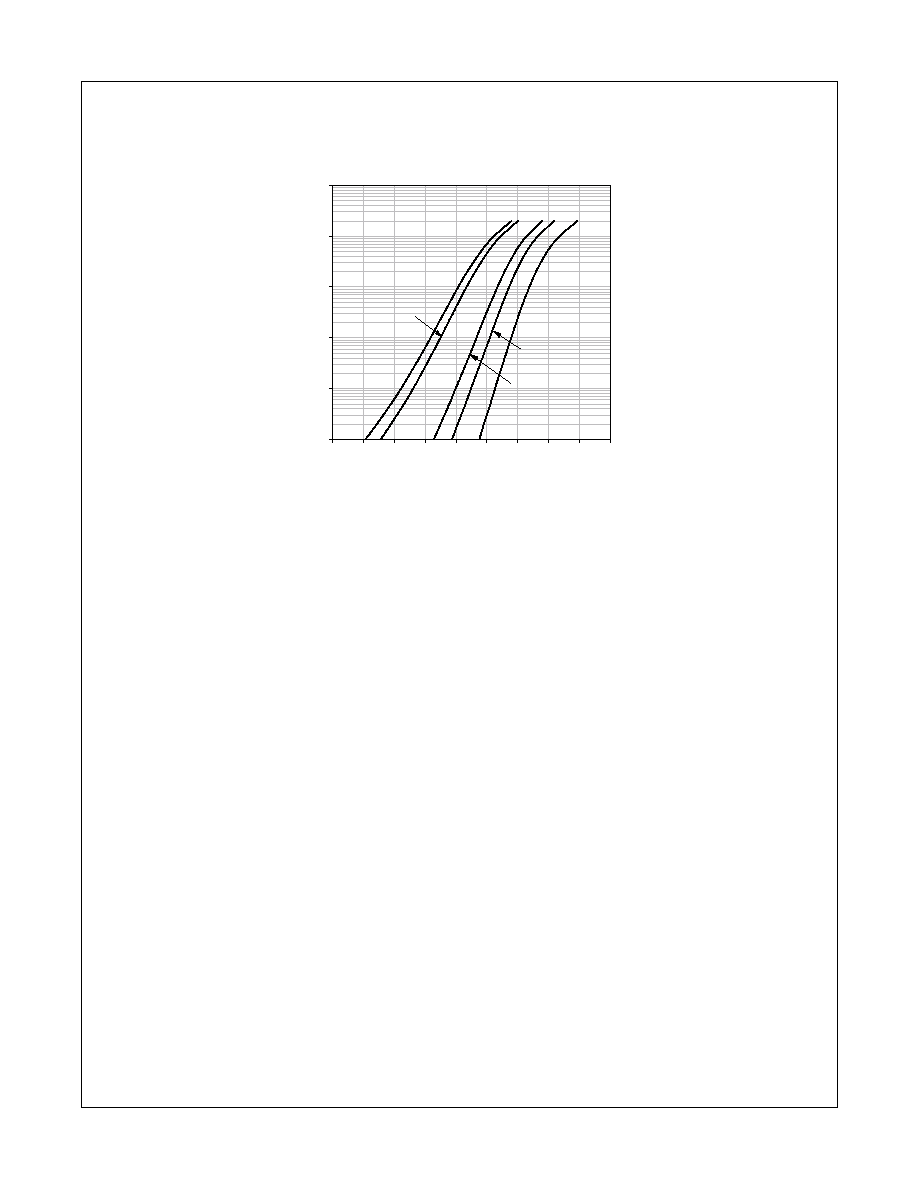
Figure 9. Input Forward Current vs. Forward Voltage
V
F
- Forward Voltage (V)
0.8
0.9
1.0
1.1
1.2
1.3
1.4
1.5
1.6
1.7
I
F
-F
orwa
r
d
Current
(m
A
)
0.001
0.01
0.1
1
10
100
T
A
= 85
o
C
T
A
= 100
o
C
T
A
= 25
o
C
T
A
= 0
o
C
T
A
= -40
o
C
7
www.fairchildsemi.com
FOD0708/FOD0738 Rev. 1.0.6
FOD0708 Single Channel CMOS Optocoupler FOD0738 Dual Channel CMOS Optocoupler
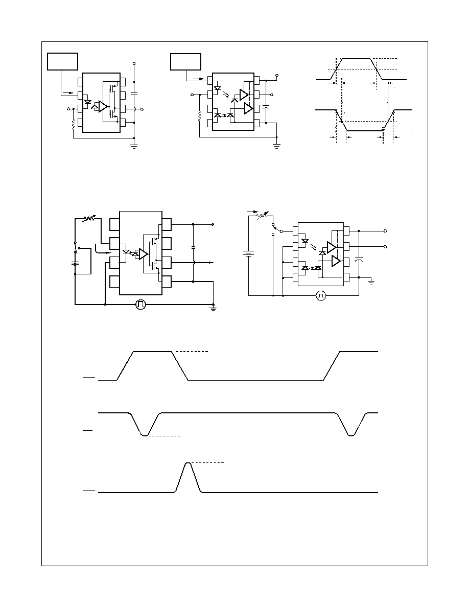
Fig. 10 Test Circuit and Waveforms for t
PLH
, t
PHL,
t
r
and t
f
.
1
2
3
4
1
2
3
4
8
7
6
5
8
7
6
5
Pulse Gen.
Z
O
= 50
t
f
= t
r
= 5 ns
Pulse Gen.
t
f
= t
r
= 5 ns
Z
O
= 50
I
F
R
IN
Vcc
Vcc
0.1
µ
F
Bypass
Input
Monitoring
Node
Input
Monitor
Node
Output
Monitoring
Node
Output
Monitoring
Node
Test Circuit for FOD0708
Test Circuit for FOD0708
Test Circuit for FOD0738
Test Circuit for FOD0738
Peak
CM
V
0V
O
V
OL
V
OH
V
Switching Pos. (A), I = 0
F
O
V (Max)
CM
O
V
Switching Pos. (B), I = 12 mA
F
H
CM
L
V (Min)
O
Fig. 11 Test Circuit Common Mode Transient Immunity
(FOD0708 and FOD0738)
I
F
+5V
3
2
1
4
8
7
6
5
GND
V
CC
O
(V )
Output
V
CM
FF
V
A
B
Pulse Gen
I
F
bypass
0.1
µ
F
1
2
3
4
8
B
A
7
6
5
Dual Channel
+5V
I
F
V
CM
Pulse
Generator
Z
O
= 50
+
V
FF
Output V
O
Monitoring
Node
0.1
µ
F
Bypass
R
IN
0.1
µ
F
PHL
t
10%
10%
90%
90%
I
F
= 12mA
2.5V CMOS
50%
PLH
t
OL
V
r
t
f
t
Output
Input
Waveforms
8
www.fairchildsemi.com
FOD0708/FOD0738 Rev. 1.0.6
FOD0708 Single Channel CMOS Optocoupler FOD0738 Dual Channel CMOS Optocoupler
8-Pin Small Outline
0.024 (0.61)
0.050 (1.27)
0.155 (3.94)
0.275 (6.99)
0.060 (1.52)
9
www.fairchildsemi.com
FOD0708/FOD0738 Rev. 1.0.6
FOD0708 Single Channel CMOS Optocoupler FOD0738 Dual Channel CMOS Optocoupler
Ordering Information
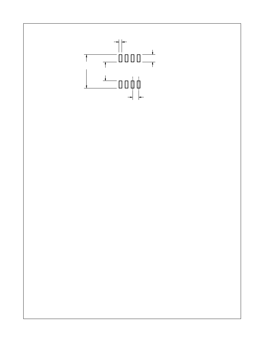
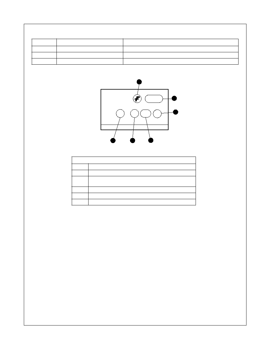
Marking Information
Option
Order Entry Identifier
Description
No Suffix
FOD0708
Shipped in tubes (50 units per tube)
R1
FOD0708R1
Tape and Reel (500 units per reel)
R2
FOD0708R2
Tape and Reel (2500 units per reel)
1
2
6
4
3
5
Definitions
1
Fairchild logo
2
Device number
3
VDE mark (Note: Only appears on parts ordered with VDE option
See order entry table)
4
One digit year code, e.g., `5'
5
Two digit work week ranging from `01' to `53'
6
Assembly package code
0708
S
YY
X
V
10
www.fairchildsemi.com
FOD0708/FOD0738 Rev. 1.0.6
FOD0708 Single Channel CMOS Optocoupler FOD0738 Dual Channel CMOS Optocoupler
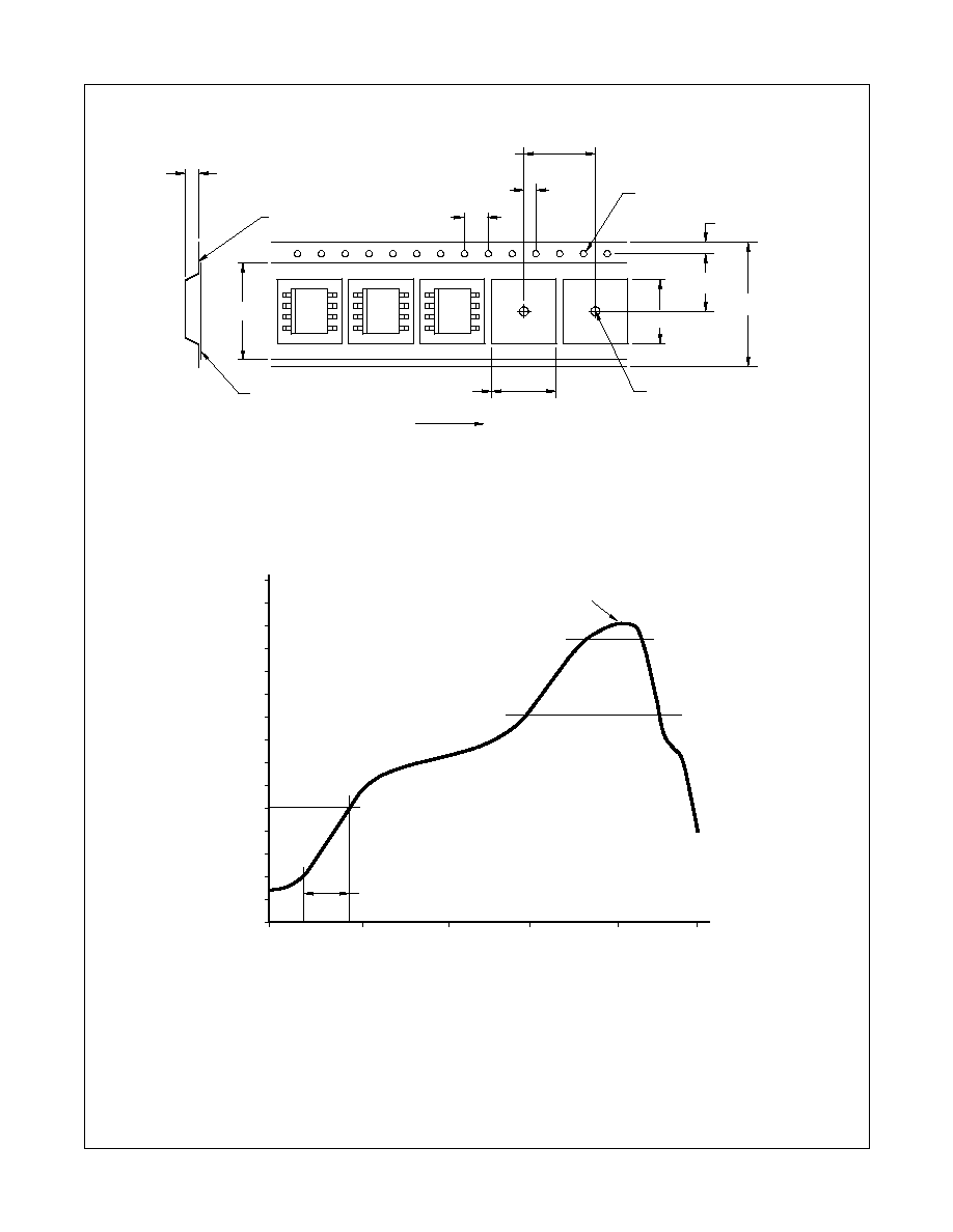
Carrier Tape Specification
Reflow Profile
4.0
±
0.10
Ø1.5 MIN
User Direction of Feed
2.0
±
0.05
1.75
±
0.10
5.5
±
0.05
12.0
±
0.3
8.0
±
0.10
0.30 MAX
8.3
±
0.10
3.50
±
0.20
0.1 MAX
6.40
±
0.20
5.20
±
0.20
Ø1.5
±
0.1/-0
300
280
260
240
220
200
180
160
140
120
100
80
60
40
20
0
°
C
Time (s)
0
60
180
120
270
260
°
C
>245
°
C = 42 Sec
Time above
183
°
C = 90 Sec
360
1.822
°
C/Sec Ramp up rate
33 Sec

11
www.fairchildsemi.com
FOD0708/FOD0738 Rev. 1.0.6
FOD0708 Single Channel CMOS Optocoupler FOD0738 Dual Channel CMOS Optocoupler
DISCLAIMER
FAIRCHILD SEMICONDUCTOR RESERVES THE RIGHT TO MAKE CHANGES WITHOUT FURTHER NOTICE TO ANY
PRODUCTS HEREIN TO IMPROVE RELIABILITY, FUNCTION OR DESIGN. FAIRCHILD DOES NOT ASSUME ANY LIABILITY
ARISING OUT OF THE APPLICATION OR USE OF ANY PRODUCT OR CIRCUIT DESCRIBED HEREIN; NEITHER DOES IT
CONVEY ANY LICENSE UNDER ITS PATENT RIGHTS, NOR THE RIGHTS OF OTHERS.
TRADEMARKS
The following are registered and unregistered trademarks Fairchild Semiconductor owns or is authorized to use and is
not intended to be an exhaustive list of all such trademarks.
LIFE SUPPORT POLICY
FAIRCHILDíS PRODUCTS ARE NOT AUTHORIZED FOR USE AS CRITICAL COMPONENTS IN LIFE SUPPORT
DEVICES OR SYSTEMS WITHOUT THE EXPRESS WRITTEN APPROVAL OF FAIRCHILD SEMICONDUCTOR CORPORATION.
As used herein:
1. Life support devices or systems are devices or
systems which, (a) are intended for surgical implant into
the body, or (b) support or sustain life, or (c) whose
failure to perform when properly used in accordance
with instructions for use provided in the labeling, can be
reasonably expected to result in significant injury to the
user.
2. A critical component is any component of a life
support device or system whose failure to perform can
be reasonably expected to cause the failure of the life
support device or system, or to affect its safety or
effectiveness.
PRODUCT STATUS DEFINITIONS
Definition of Terms
Datasheet Identification
Product Status
Definition
Advance Information
Preliminary
No Identification Needed
Obsolete
This datasheet contains the design specifications for
product development. Specifications may change in
any manner without notice.
This datasheet contains preliminary data, and
supplementary data will be published at a later date.
Fairchild Semiconductor reserves the right to make
changes at any time without notice in order to improve
design.
This datasheet contains final specifications. Fairchild
Semiconductor reserves the right to make changes at
any time without notice in order to improve design.
This datasheet contains specifications on a product
that has been discontinued by Fairchild semiconductor.
The datasheet is printed for reference information only.
Formative or
In Design
First Production
Full Production
Not In Production
ISOPLANARTM
LittleFETTM
MICROCOUPLERTM
MicroFETTM
MicroPakTM
MICROWIRETM
MSXTM
MSXProTM
OCXTM
OCXProTM
OPTOLOGIC
®
OPTOPLANARTM
PACMANTM
POPTM
Power247TM
PowerEdgeTM
FAST
®
FASTrTM
FPSTM
FRFETTM
GlobalOptoisolatorTM
GTOTM
HiSeCTM
I
2
CTM
i-LoTM
ImpliedDisconnectTM
IntelliMAXTM
Rev. I17
ACExTM
ActiveArrayTM
BottomlessTM
Build it NowTM
CoolFETTM
CROSSVOLTTM
DOMETM
EcoSPARKTM
E
2
CMOSTM
EnSignaTM
FACTTM
FACT Quiet SeriesTM
PowerSaverTM
PowerTrench
®
QFET
®
QSTM
QT OptoelectronicsTM
Quiet SeriesTM
RapidConfigureTM
RapidConnectTM
µSerDesTM
ScalarPumpTM
SILENT SWITCHER
®
SMART STARTTM
SPMTM
StealthTM
SuperFETTM
SuperSOTTM-3
SuperSOTTM-6
SuperSOTTM-8
SyncFETTM
TinyLogic
®
TINYOPTOTM
TruTranslationTM
UHCTM
UltraFET
®
UniFETTM
VCXTM
WireTM
Across the board. Around the world.TM
The Power Franchise
®
Programmable Active DroopTM