 | ÐлекÑÑоннÑй компоненÑ: FOD070L | СкаÑаÑÑ:  PDF PDF  ZIP ZIP |
Äîêóìåíòàöèÿ è îïèñàíèÿ www.docs.chipfind.ru
8/10/04
Page 1 of 17
© 2004 Fairchild Semiconductor Corporation
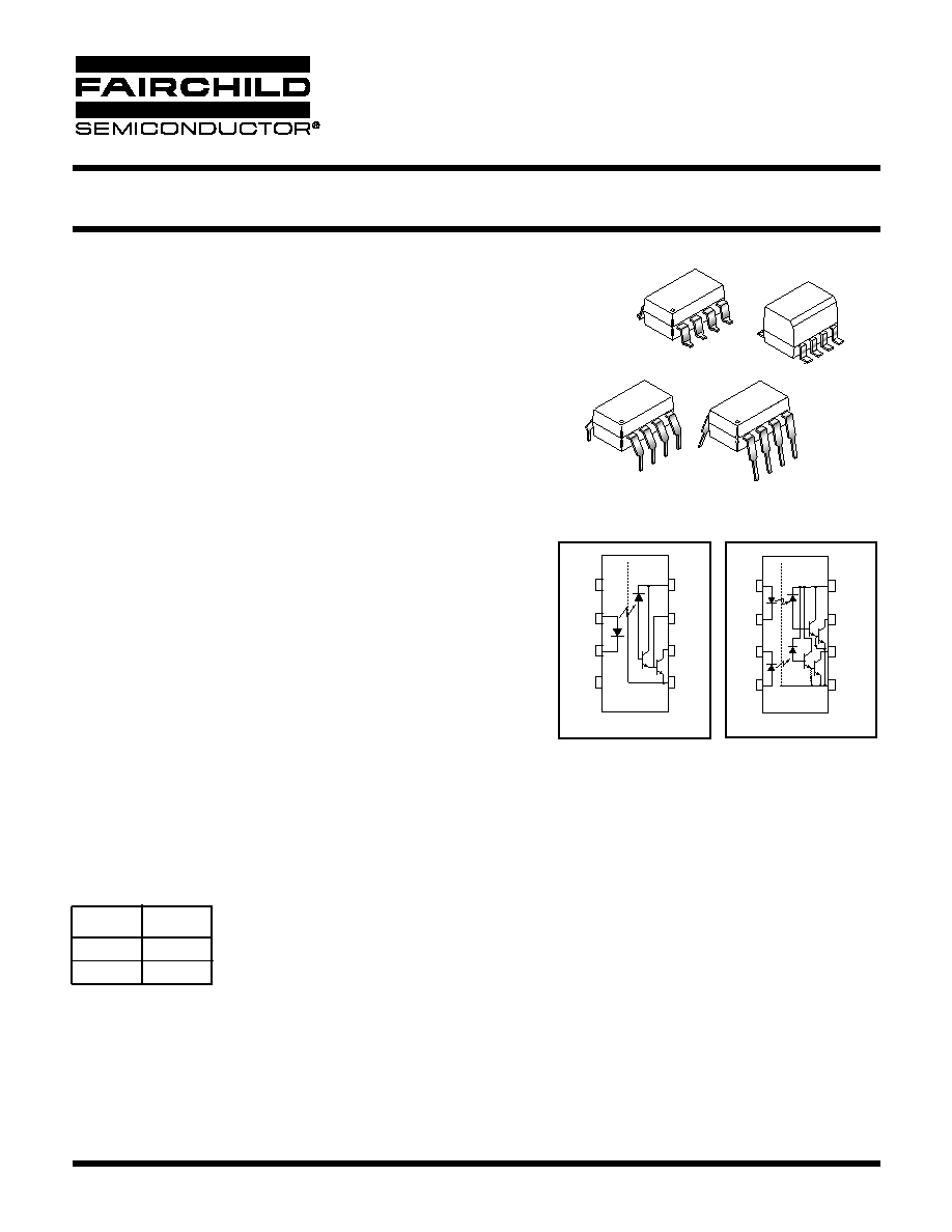
LVTTL/LVCMOS COMPATIBLE LOW INPUT
CURRENT HIGH GAIN SPLIT DARLINGTON
OPTOCOUPLERS
SINGLE CHANNEL:
FOD070L
FOD270L
DUAL CHANNEL:
FOD073L
DESCRIPTION
The FOD070L, FOD270L and FOD073L optocouplers consist of an AlGaAs
LED optically coupled to a high gain split darlington photodetector. These
devices are specified to operate at a 3.3V supply voltage.
The split darlington configuration separating the input photodiode and the first
stage gain from the output transistor permits lower output saturation voltage
and higher speed operation than possible with conventional darlington
phototransistor optocoupler. In the dual channel device FOD073L, an inte-
grated emitter base resistor provides superior stability over temperature.
The combination of a very low input current of 0.5 mA and a high current
transfer ratio of 2000% makes this family particularly useful for input interface
to MOS, CMOS, LSTTL and EIA RS232C, while output compatibility is
ensured to LVCMOS as well as high fan-out LVTTL requirements.
An internal noise shield provides exceptional common mode rejection of
10 kV/µs.
FEATURES
·
Low power consumption
·
Low input current - 0.5 mA
·
Available in single channel 8-pin DIP (FOD270L), 8-pin SOIC (FOD070L)
and dual channel 8-pin SOIC
·
High CTR-2000%
·
High CMR-10 kV/µs
·
Guaranteed performance over temperature 0°C to 70°C
·
U.L. recognized (File # E90700)
·
LVTTL/LVCMOS Compatible output
APPLICATIONS
·
Digital logic ground isolation LVTTL/LVCMOS
·
Telephone ring detector
·
EIA-RS-232C line receiver
·
High common mode noise line receiver
·
µP bus isolation
·
Current loop receiver
TRUTH TABLE
LED
V
O
ON
LOW
OFF
HIGH
8
8
1
8
1
1
1
2
3
4
5
6
7
8
+
_
V
F
V
CC
V
B
V
O
GND
FOD070L / FOD270L
N/C
N/C
1
2
3
4
5
6
7
8
+
_
V
F1
V
CC
V
01
V
02
GND
FOD073L
V
F2
_
+
8/10/04
Page 2 of 17
© 2004 Fairchild Semiconductor Corporation
LVTTL/LVCMOS COMPATIBLE LOW INPUT
CURRENT HIGH GAIN SPLIT DARLINGTON
OPTOCOUPLERS
SINGLE CHANNEL:
FOD070L
FOD270L
DUAL CHANNEL:
FOD073L
**All typicals at T
A
= 25°C
ABSOLUTE MAXIMUM RATINGS
(No derating required up to 85°C)
Parameter
Symbol
Value
Units
Storage Temperature
T
STG
-40 to +125
°C
Operating Temperature
T
OPR
-40 to +85
°C
Lead Solder Temperature (Wave solder only. See reflow profile for surface
mount devices)
T
SOL
260 for 10 sec
°C
EMITTER
DC/Average Forward Input Current
Each Channel
I
F
(avg)
20
mA
Peak Forward Input Current (50% duty cycle, 1 ms P.W.)
Each Channel
I
F
(pk)
40
mA
Peak Transient Input Current - (
1 µs P.W., 300 pps)
Each Channel
I
F
(trans)
1.0
A
Reverse Input Voltage
Each Channel
V
R
5
V
Input Power Dissipation
Each Channel
P
D
35
mW
DETECTOR
Average Output Current
Each Channel
I
O
(avg)
60
mA
Emitter-Base Reverse Voltage (FOD070L, FOD270L)
Each Channel
V
EB
0.5
V
Supply Voltage, Output Voltage
Each Channel
V
CC
,
V
O
-0.5 to 7
V
Output power dissipation
Each Channel
P
D
100
mW
ELECTRICAL CHARACTERISTICS
(T
A
= 0 to 70°C Unless otherwise specified)
INDIVIDUAL COMPONENT CHARACTERISTICS
Parameter
Test Conditions
Symbol
Device
Min
Typ**
Max
Unit
EMITTER
T
A
=25°C
V
F
All
1.35
1.7
V
Input Forward Voltage
Each Channel (I
F
= 1.6 mA)
1.75
Input Reverse Breakdown
Voltage
(T
A
=25°C, I
R
= 10 µA)
BV
R
All
5.0
V
Each Channel
DETECTOR
Logic high output current
(I
F
= 0 mA, V
O
= V
CC
= 3.3 V)
I
OH
FOD070L
FOD270L
0.05
25
µA
Each Channel
FOD073L
Logic Low Supply
Current
I
F
= 1.6 mA, V
O
= Open, V
CC
= 3.3V
I
CCL
FOD070L
FOD270L
0.5
1.5
mA
FOD073L
0.8
3
I
F1
= I
F2
= 1.6mA
V
O1
= V
O2
= Open, V
CC
= 3.3 V
Logic High Supply
Current
I
F
= 0 mA, V
O
= Open, V
CC
= 3.3V
I
CCH
FOD070L
FOD270L
0.01
1
µA
FOD073L
0.01
2
I
F1
= I
F2
= 0mA
V
O1
= V
O2
= Open, V
CC
= 3.3 V

8/10/04
Page 3 of 17
© 2004 Fairchild Semiconductor Corporation
LVTTL/LVCMOS COMPATIBLE LOW INPUT
CURRENT HIGH GAIN SPLIT DARLINGTON
OPTOCOUPLERS
SINGLE CHANNEL:
FOD070L
FOD270L
DUAL CHANNEL:
FOD073L
**All typicals at T
A
= 25°C
** All typicals at TA = 25°C
TRANSFER CHARACTERISTICS
(T
A
= 0 to 70°C Unless otherwise specified)
Parameter
Test Conditions Symbol
Device
Min
Typ**
Max
Unit
COUPLED
Current transfer ratio
(Notes 1,2)
(I
F
= 0.5 mA, V
O
= 0.4 V, V
CC
= 3.3V)
CTR
ALL
400
7000
%
Logic low output voltage
output voltage
(Note 2)
(I
F
= 1.6 mA, I
O
= 8 mA, V
CC
= 3.3V)
V
OL
ALL
0.07
0.3
V
(I
F
= 5 mA, I
O
= 15 mA, V
CC
= 3.3V)
ALL
0.07
0.4
SWITCHING CHARACTERISTICS
(T
A
= 0 to 70°C unless otherwise specified., V
CC
= 3.3 V)
Parameter
Test Conditions
Symbol
Device
Min
Typ**
Max
Unit
Propagation delay
time to logic low
(R
L
= 4.7 k
, I
F
= 0.5 mA)
(Note 2) (Fig. 17)
T
PHL
FOD070L
FOD270L
3
30
µs
FOD073L
5
Propagation delay
time to logic high
(R
L
= 4.7 k
, I
F
= 0.5 mA)
(Note 2) (Fig. 17)
T
PLH
FOD070L
FOD270L
50
90
µs
FOD073L
25
Common mode transient
immunity at logic high
(I
F
= 0 mA, |V
CM
| = 10 V
P-P
)
T
A
= 25°C (R
L
= 2.2 k
) (Note 3) (Fig. 18)
|CM
H
|
ALL
1,000
10,000
V/µs
Common mode transient
immunity at logic low
(I
F
= 1.6 mA, |V
CM
| = 10 V
P-P
,
R
L
= 2.2 k
)
T
A
= 25°C (Note 3) (Fig. 18)
|CM
L
|
ALL
1,000
10,000
V/µs
8/10/04
Page 4 of 17
© 2004 Fairchild Semiconductor Corporation
LVTTL/LVCMOS COMPATIBLE LOW INPUT
CURRENT HIGH GAIN SPLIT DARLINGTON
OPTOCOUPLERS
SINGLE CHANNEL:
FOD070L
FOD270L
DUAL CHANNEL:
FOD073L
** All typicals at T
A
= 25°C
1. Current Transfer Ratio is defined as a ratio of output collector current, I
O
, to the forward LED input current, I
F
, times 100%.
2. Pin 7 open. (FOD070L and FOD270L only)
3. Common mode transient immunity in logic high level is the maximum tolerable (positive) dV
CM
/dt on the leading edge of the
common mode pulse signal, V
CM
, to assure that the output will remain in a logic high state (i.e., V
O
>2.0 V). Common mode
transient immunity in logic low level is the maximum tolerable (negative) dV
CM
/dt on the trailing edge of the common mode
pulse signal, V
CM
, to assure that the output will remain in a logic low state (i.e., V
O
<0.8 V).
4. Device is considered a two terminal device: Pins 1, 2, 3 and 4 are shorted together and Pins 5, 6, 7 and 8 are shorted together.
5. For dual channel devices, CI-O is measured by shorting pins 1 and 2 or pins 3 and 4 together and pins 5 through 8 shorted
together.
6. Measured between pins 1 and 2 shorted together, and pins 3 and 4 shorted together.
ISOLATION CHARACTERISTICS
(T
A
= 0 to 70°C Unless otherwise specified)
Characteristics
Test Conditions Symbol
Device
Min
Typ**
Max
Unit
Input-output
insulation leakage current
(Relative humidity = 45%)
(T
A
= 25°C, t = 5 s)
(V
I-O
= 3000 VDC)
(Note 4)
I
I-O
ALL
1.0
µA
Withstand insulation
test voltage
(R
H
50%, T
A
= 25°C)
(Note 4) ( t = 1 min.)
V
ISO
FOD070L
FOD073L
2500
V
RMS
FOD270L
5000
Resistance (input to output)
(Note 4) (V
I-O
= 500 VDC)
R
I-O
ALL
10
12
Capacitance (input to output)
(Note 4,5) (f = 1 MHz)
C
I-O
ALL
0.7
pF
Input-Input
Insulation leakage current
(RH
45%, V
I-I
= 500 VDC (Note 6)
I
I-I
FOD073L
0.005
µA
Input-Input Resistance
(V
I-I
= 500 VDC) (Note 6)
R
I-I
FOD073L
10
11
Input-Input Capacitance
(f = 1 MHz) (Note 6)
C
I-I
FOD073L
0.03
pF
NOTES
8/10/04
Page 5 of 17
© 2004 Fairchild Semiconductor Corporation
LVTTL/LVCMOS COMPATIBLE LOW INPUT
CURRENT HIGH GAIN SPLIT DARLINGTON
OPTOCOUPLERS
SINGLE CHANNEL:
FOD070L
FOD270L
DUAL CHANNEL:
FOD073L
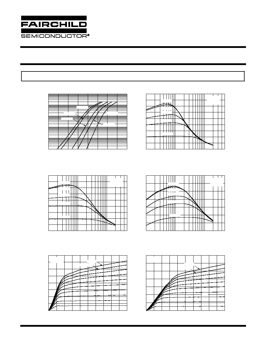
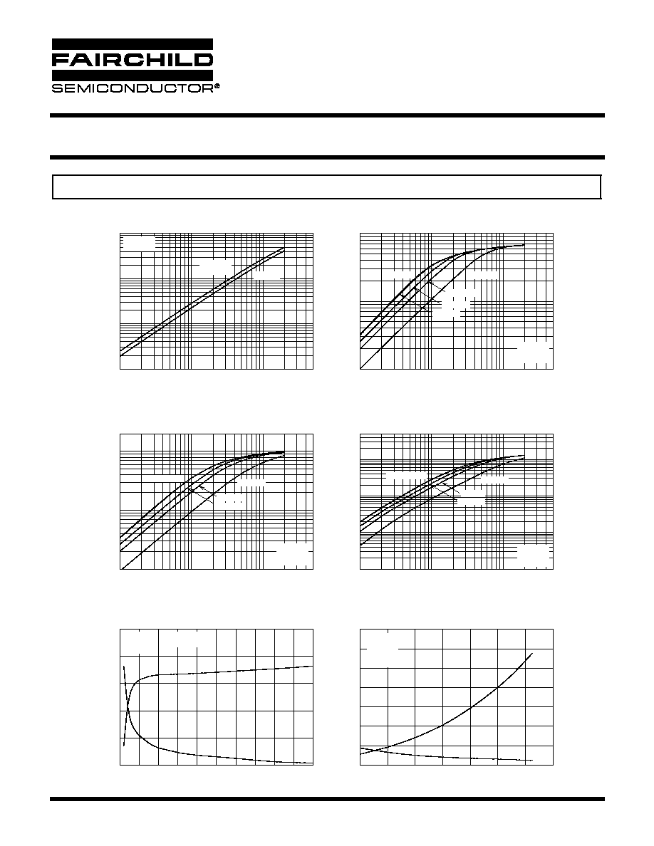
TYPICAL PERFORMANCE CURVES
Fig. 1 Input Forward Current vs Forward Voltage
Fig. 2 Current Transfer Ratio vs. Input Forward Current
(FOD270L only)
V
F
- FORWARD VOLTAGE (V)
1.1
1.0
0.9
1.2
1.3
1.4
1.5
1.6
1.7
I
F
- FOR
W
ARD CURRENT (mA)
0.001
0.01
0.1
1
10
100
I
F
- FORWARD CURRENT (mA)
1
10
0.1
CTR - CURRENT
TRANSFER RA
TIO (%)
0
500
1000
1500
2000
2500
3000
3500
4000
4500
V
O
- OUTPUT VOLTAGE (V)
0.0
0.2
0.4
0.6
0.8
1.0
1.2
1.4
1.6
1.8
2.0
0
20
40
60
80
100
120
140
Fig. 6 DC Transfer Characterstics (FOD073L only)
I
O
- OUTPUT CURRENT (mA)
T
A
= 85
°C
T
A
= 70
°C
T
A
= 25
°C
T
A
= -40
°C
T
A
= 0
°C
4mA
3.5mA
2.5mA
0.5mA
3mA
2mA
1mA
T
A
= 25
°C
V
CC
= 3.3V
I
F
= 5mA
I
F
= 4.5mA
1.5mA
Fig. 5 DC Transfer Charactersitics (FOD070L, FOD270L)
V
O
- OUTPUT VOLTAGE (V)
0.0
0.2
0.4
0.6
0.8
1.0
1.2
1.4
1.6
1.8
2.0
I
O
- OUTPUT CURRENT (mA)
0
20
40
60
80
100
120
140
160
T
A
= 25
°C
V
CC
= 3.3V
I
F
= 5mA
I
F
= 4.5mA
4mA
3.5mA
2.5mA
1.5mA
0.5mA
3mA
2mA
1mA
V
O
= 0.4V
V
CC
= 3.3V
T
A
= 25
°C
T
A
= 85
°C
T
A
= 70
°C
T
A
= 25
°C
T
A
= 0
°C
T
A
= -40
°C
Fig. 3 Current Transfer Ratio vs. Input Forward Current
(FOD070L only)
Fig. 4 Current Transfer Ratio vs. Input Forward Current
(FOD073L only)
I
F
- FORWARD CURRENT (mA)
1
10
0.1
CTR - CURRENT
TRANSFER RA
TIO (%)
0
500
1000
1500
2000
2500
3000
3500
4000
4500
I
F
- FORWARD CURRENT (mA)
1
10
0.1
CTR - CURRENT
TRANSFER RA
TIO (%)
0
500
1000
1500
2000
2500
3000
3500
V
O
= 0.4V
V
CC
= 3.3V
T
A
= 25
°C
T
A
= 85
°C
T
A
= 70
°C
T
A
= 25
°C
T
A
= 0
°C
T
A
= -40
°C
V
O
= 0.4V
V
CC
= 3.3V
T
A
= 25
°C
T
A
= 85
°C
T
A
= 70
°C
T
A
= 25
°C
T
A
= 0
°C
T
A
= -40
°C
8/10/04
Page 6 of 17
© 2004 Fairchild Semiconductor Corporation
LVTTL/LVCMOS COMPATIBLE LOW INPUT
CURRENT HIGH GAIN SPLIT DARLINGTON
OPTOCOUPLERS
SINGLE CHANNEL:
FOD070L
FOD270L
DUAL CHANNEL:
FOD073L
TYPICAL PERFORMANCE CURVES
Fig. 7 Supply Current vs Input Forward Current
Fig. 8 Output Current vs Input Forward Current
(FOD270L only)
(FOD270L, FOD070L, FOD073L)
I
F
- Input Forward Current (mA)
0.1
1
10
I
CC
- (P
er Channel) - Supply Current (mA)
0.01
0.1
1
10
I
F
- Input Forward Current (mA)
0.1
1
10
I
O
- Output Current (mA)
1
10
100
Fig. 9 Output Current vs Input Forward Current
(FOD070L only)
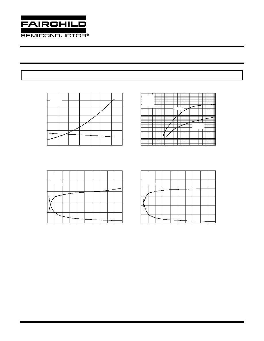
Fig. 11 Propagation Delay vs.
Input Forward Current (FOD070L only)
Fig. 12 Propagation Delay vs.
Ambient Temperature (FOD073L only)
Fig. 10 Output Current vs Input Forward Current
(FOD073L only)
I
F
- Forward Current (mA)
I
F
- Input Forward Current (mA)
0.1
1
10
I
O
- Output Current (mA)
1
10
100
0
1
2
3
4
5
6
7
8
9
10
T
A
- Ambient Temperature (
°C)
-40
-20
0
20
40
60
80
100
t
PHL
- Propagation Dela
y
T
o
Logic Lo
w (
µ
s)
t
P
- Propagation Dela
y (
µ
s)
t
PLH
- Propagation Dela
y
T
o
Logic High (
µ
s)
0
4
3
2
1
5
44
52
50
48
46
54
I
F
- Forward Current (mA)
0.1
1
10
I
O
- Output Current (mA)
0.1
10
1
100
T
A
= 25
°C
V
CC
= 3.3V
FOD270L
or FOD070L
FOD073L
V
O
= 0.4V
V
CC
= 3.3V
T
A
= 25
°C
T
A
= 85
°C
T
A
= -40
°C
T
A
= 0
°C
T
A
= 25
°C
T
A
= 70
°C
V
O
= 0.4V
V
CC
= 3.3V
T
A
= 25
°C
T
A
= -40
°C
T
A
= 70
°C, 85°C
T
A
= 0
°C
T
A
= 25
°C
t
PLH
t
PLH
t
PHL
t
PHL
0
40
30
20
10
50
60
70
V
O
= 0.4V
V
CC
= 3.3V
T
A
= 25
°C
T
A
= -40
°C
T
A
= 70
°C, 85°C
T
A
= 0
°C
T
A
= 25
°C
T
A
= 25
°C
V
CC
= 3.3V
R
L
= 4.7k
1/f = 100
µs
Duty Cycle = 10%
V
CC
= 3.3V
IF = 0.5mA
R
L
= 4.7k
1/f = 100
µs
Duty Cycle = 10%
8/10/04
Page 7 of 17
© 2004 Fairchild Semiconductor Corporation
LVTTL/LVCMOS COMPATIBLE LOW INPUT
CURRENT HIGH GAIN SPLIT DARLINGTON
OPTOCOUPLERS
SINGLE CHANNEL:
FOD070L
FOD270L
DUAL CHANNEL:
FOD073L
TYPICAL PERFORMANCE CURVES
Fig. 13 Propagation Delay vs.
Ambient Temperature (FOD070L, FOD270L)
Fig. 14 Propagation Delay To Logic Low vs Pulse Period
(FOD073L, FOD070L, FOD270L)
T
A
- Ambient Temperature (
°C)
T - Pulse Period (ms)
-40
0.01
0.1
1
10
-20
0
20
40
60
80
100
t
PHL
- Propagation Dela
y to Logic Lo
w (
µ
s)
t
PLH
- Propagation Dela
y to Logic High (
µ
s)
t
PLH
t
PLH
t
PLH
t
PHL
t
PHL
t
PHL
0
8
6
4
2
10
12
14
t
PHL
- Propagation Dela
y to Logic Lo
w (
µ
s)
1
10
100
0
80
60
40
20
100
120
140
Fig. 15 Propagation Delay vs.
Input Forward Current (FOD270L only)
Fig. 16 Propagation Delay vs.
Input Forward Current (FOD073L only)
I
F
- Input Forward Current (mA)
I
F
- Input Forward Current (mA)
0
1
2
3
4
5
6
7
8
9
10
t
PHL
- Propagation Dela
y to Logic Lo
w (
µ
s)
t
PLH
- Propagation Dela
y to Logic High (
µ
s)
0
2
1
3
4
5
42
50
48
46
44
52
0
1
2
3
4
5
6
7
8
9
10
t
PHL
- Propagation Dela
y to Logic Lo
w (
µ
s)
t
PLH
- Propagation Dela
y to Logic High (
µ
s)
0
4
2
6
8
12
10
16
24
22
20
18
26
28
V
CC
= 3.3V
IF = 0.5mA
R
L
= 4.7k
1/f = 200
µs
Duty Cycle = 10%
T
A
= 25
°C
V
CC
= 3.3V
I = 0.5mA
R
L
= 4.7k
Duty Cycle = 50
µs
FOD070L,
FOD270L
FOD073L
T
A
= 25
°C
V
CC
= 3.3V
R
L
= 4.7k
1/f = 100
µs
Duty Cycle = 10%
T
A
= 25
°C
V
CC
= 3.3V
R
L
= 4.7k
1/f = 100
µs
Duty Cycle = 10%

8/10/04
Page 8 of 17
© 2004 Fairchild Semiconductor Corporation
LVTTL/LVCMOS COMPATIBLE LOW INPUT
CURRENT HIGH GAIN SPLIT DARLINGTON
OPTOCOUPLERS
SINGLE CHANNEL:
FOD070L
FOD270L
DUAL CHANNEL:
FOD073L
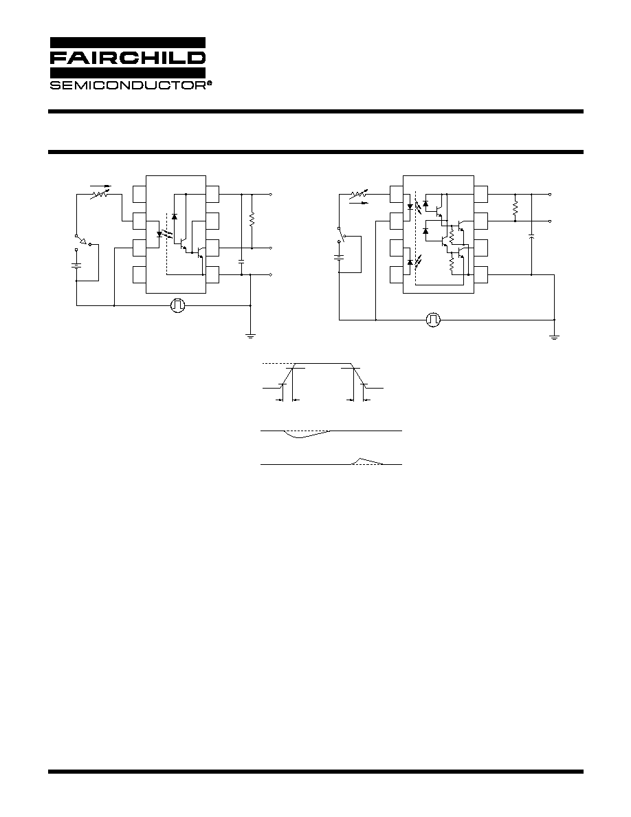
Fig. 17 Switching Time Test Circuit
T
T
PLH
OL
V
O
V
O
3.3 V
50%
F
I
50%
T
PHL
T
4
5
Noise
1
2
3
Shield
8
7
6
O
V
V
CC
V
01
V
02
GND
V
F1
-
+
F2
V
F
I
+
F
I
MONITOR
L
R
0.1
µF
Pulse
Generator
tr = 5ns
Z = 50
O
V
3
I Monitor
F
4
tr = 5ns
Generator
Pulse
Z = 50
O
V
F
V
V
I
V
F
2
1
V
O
V
V
O
6
5
GND
7
8
V
O
B
V
B
L
R
CC
V
C
+3.3 V
+3.3 V
0.1
µF
C = 15 pF*
L
Test Circuit for FOD073L
Test Circuit for FOD070L, FOD270L
*Includes Probe and Fixture Capacitance
m
R
Rm
Shield
Noise
-
C = 15 pF*
8/10/04
Page 9 of 17
© 2004 Fairchild Semiconductor Corporation
LVTTL/LVCMOS COMPATIBLE LOW INPUT
CURRENT HIGH GAIN SPLIT DARLINGTON
OPTOCOUPLERS
SINGLE CHANNEL:
FOD070L
FOD270L
DUAL CHANNEL:
FOD073L
Fig. 18 Common Mode Immunity Test Circuit
Test Circuit for FOD073L
Test Circuit for FOD070L and FOD270L
Pulse Gen
CM
V
V
FF
B
A
+
-
+3.3 V
O
V
-
I
F
3
4
F
V
2
1
Shield
Noise
6
O
5
GND
7
8
V
B
V
CC
V
L
R
Switch at A : I = 0 mA
F
Switch at B : I = 1.6 mA
F
t
r
V
O
O
V
OL
V
3.3 V
0 V
10%
10%
90%
CM
V 10 V
GND
+
-
F2
V
V
F1
-
+3.3 V
CC
V
L
V
02
V
R
01
V
O
V
CM
A
B
Pulse Gen
F
I
+
-
+
0.1
µF
f
t
FF
V
90%
1
3
4
2
Shield
Noise
8
6
5
7
0.1
µF
8/10/04
Page 10 of 17
© 2004 Fairchild Semiconductor Corporation
LVTTL/LVCMOS COMPATIBLE LOW INPUT
CURRENT HIGH GAIN SPLIT DARLINGTON
OPTOCOUPLERS
SINGLE CHANNEL:
FOD070L
FOD270L
DUAL CHANNEL:
FOD073L
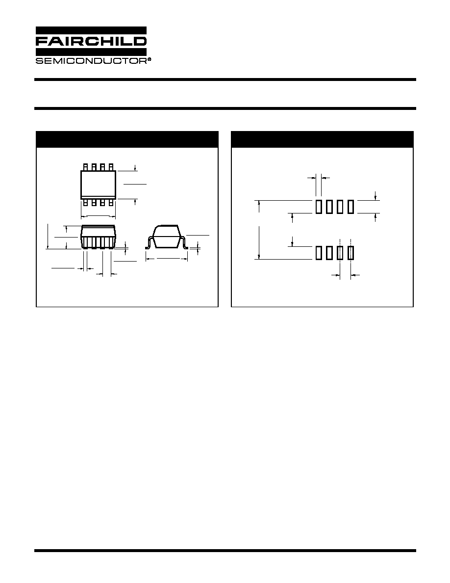
Package Dimensions (Through Hole)
0.200 (5.08)
0.140 (3.55)
0.100 (2.54) TYP
0.022 (0.56)
0.016 (0.41)
0.020 (0.51) MIN
0.390 (9.91)
0.370 (9.40)
0.270 (6.86)
0.250 (6.35)
3
0.070 (1.78)
0.045 (1.14)
2
4
1
5
6
7
8
0.300 (7.62)
TYP
0.154 (3.90)
0.120 (3.05)
0.016 (0.40)
0.008 (0.20)
15° MAX
PIN 1
ID.
SEATING PLANE
Package Dimensions (Surface Mount)
Lead Coplanarity : 0.004 (0.10) MAX
0.270 (6.86)
0.250 (6.35)
0.390 (9.91)
0.370 (9.40)
0.022 (0.56)
0.016 (0.41)
0.100 (2.54)
TYP
0.020 (0.51)
MIN
0.070 (1.78)
0.045 (1.14)
0.300 (7.62)
TYP
0.405 (10.30)
MIN
0.315 (8.00)
MIN
0.045 [1.14]
3
2
1
4
5
6
7
8
0.016 (0.41)
0.008 (0.20)
PIN 1
ID.
Package Dimensions (0.4"Lead Spacing)
0.200 (5.08)
0.140 (3.55)
0.100 (2.54) TYP
0.022 (0.56)
0.016 (0.41)
0.004 (0.10) MIN
0.390 (9.91)
0.370 (9.40)
0.270 (6.86)
0.250 (6.35)
3
0.070 (1.78)
0.045 (1.14)
2
4
1
5
6
7
8
0.400 (10.16)
TYP
0.154 (3.90)
0.120 (3.05)
0.016 (0.40)
0.008 (0.20)
0° to 15°
PIN 1
ID.
SEATING PLANE
Recommend Pad Layout for
Surface Mount Leadform
0.070 (1.78)
0.060 (1.52)
0.030 (0.76)
0.100 (2.54)
0.295 (7.49)
0.415 (10.54)
NOTE
All dimensions are in inches (millimeters)
8-Pin DIP
8/10/04
Page 11 of 17
© 2004 Fairchild Semiconductor Corporation
LVTTL/LVCMOS COMPATIBLE LOW INPUT
CURRENT HIGH GAIN SPLIT DARLINGTON
OPTOCOUPLERS
SINGLE CHANNEL:
FOD070L
FOD270L
DUAL CHANNEL:
FOD073L
SOIC 8
Package Dimensions (Surface Mount)
Lead Coplanarity : 0.004 (0.10) MAX
0.202 (5.13)
0.182 (4.63)
0.021 (0.53)
0.011 (0.28)
0.050 (1.27)
TYP
0.164 (4.16)
0.144 (3.66)
0.244 (6.19)
0.224 (5.69)
0.143 (3.63)
0.123 (3.13)
0.008 (0.20)
0.003 (0.08)
0.010 (0.25)
0.006 (0.16)
SEAT
ING PLANE
Recommend Pad Layout
0.024 (0.61)
0.050 (1.27)
0.155 (3.94)
0.275 (6.99)
0.060 (1.52)

8/10/04
Page 12 of 17
© 2004 Fairchild Semiconductor Corporation
LVTTL/LVCMOS COMPATIBLE LOW INPUT
CURRENT HIGH GAIN SPLIT DARLINGTON
OPTOCOUPLERS
SINGLE CHANNEL:
FOD070L
FOD270L
DUAL CHANNEL:
FOD073L
ORDERING INFORMATION
MARKING INFORMATION (FOD070L, FOD073L)
Option
Order Entry Identifier
Description
S
FOD270LS
Surface Mount Lead Bend (DIP Package Only)
SD
FOD270LSD
Surface Mount; Tape and reel (DIP Package Only)
(1000 units per reel)
SV
Pending approval
Surface Mount; VDE 0884 (DIP Package Only)
SDV
Pending approval
Surface Mount; Tape and reel (DIP Package Only); VDE 0884
(1000 units per reel)
T
FOD270LT
0.4" lead spacing (DIP Package Only)
TV
Pending approval
0.4" lead spacing, VDE 0884 (DIP Package Only)
R1
FOD070LR1
Tape and reel (500 units per reel) (SOIC 8 Package only)
R1V
Pending approval
VDE, Tape and reel (500 units per reel) (SOIC 8 Package only)
R2
FOD070LR2
Tape and reel (2500 units per reel) (SOIC 8 Package only)
R2V
Pending approval
VDE 0884, Tape and reel (2500 units per reel) (SOIC 8 Package only)
V
Pending approval
VDE 0884
1
2
6
4
3
5
Definitions
1
Fairchild logo
2
Device number
3
VDE mark (Note: Only appears on parts ordered with VDE
option See order entry table)
4
One digit year code, e.g., `3'
5
Two digit work week ranging from `01' to `53'
6
Assembly package code
70L
S
YY
X
V
8/10/04
Page 13 of 17
© 2004 Fairchild Semiconductor Corporation
LVTTL/LVCMOS COMPATIBLE LOW INPUT
CURRENT HIGH GAIN SPLIT DARLINGTON
OPTOCOUPLERS
SINGLE CHANNEL:
FOD070L
FOD270L
DUAL CHANNEL:
FOD073L
MARKING INFORMATION (FOD270L)
1
2
6
4
3
5
270L
B
YY
XX
V
Definitions
1
Fairchild logo
2
Device number
3
VDE mark (Note: Only appears on parts ordered with VDE
option See order entry table)
4
Two digit year code, e.g., `03'
5
Two digit work week ranging from `01' to `53'
6
Assembly package code
8/10/04
Page 14 of 17
© 2004 Fairchild Semiconductor Corporation
LVTTL/LVCMOS COMPATIBLE LOW INPUT
CURRENT HIGH GAIN SPLIT DARLINGTON
OPTOCOUPLERS
SINGLE CHANNEL:
FOD070L
FOD270L
DUAL CHANNEL:
FOD073L
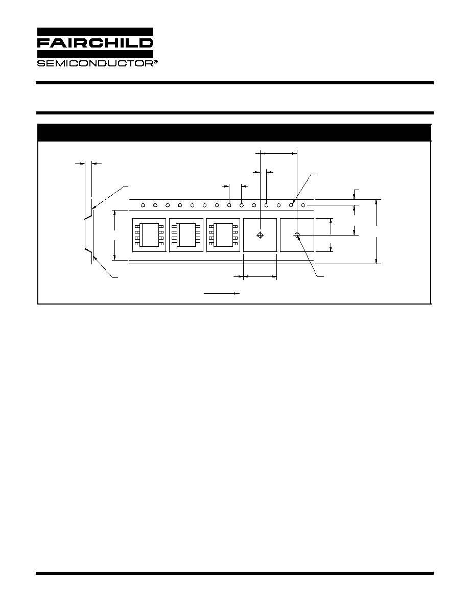
Carrier Tape Specifications (FOD070L and FOD073L)
4.0
± 0.10
Ø1.5 MIN
User Direction of Feed
2.0
± 0.05
1.75
± 0.10
5.5
± 0.05
12.0
± 0.3
8.0
± 0.10
0.30 MAX
8.3
± 0.10
3.50
± 0.20
0.1 MAX
6.40
± 0.20
5.20
± 0.20
Ø1.5
± 0.1/-0
8/10/04
Page 15 of 17
© 2004 Fairchild Semiconductor Corporation
LVTTL/LVCMOS COMPATIBLE LOW INPUT
CURRENT HIGH GAIN SPLIT DARLINGTON
OPTOCOUPLERS
SINGLE CHANNEL:
FOD070L
FOD270L
DUAL CHANNEL:
FOD073L
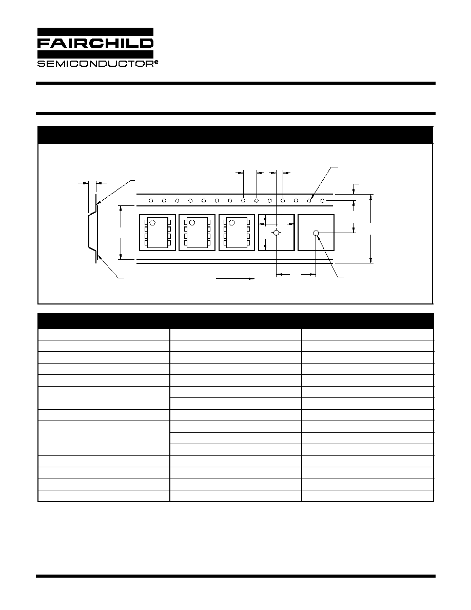
Carrier Tape Specifications (FOD270L)
Description
Symbol
Dimension in mm
Tape Width
W
16.0 ± 0.3
Tape Thickness
t
0.30 ± 0.05
Sprocket Hole Pitch
P
0
4.0 ± 0.1
Sprocket Hole Diameter
D
0
1.55 ± 0.05
Sprocket Hole Location
E
1.75 ± 0.10
Pocket Location
F
7.5 ± 0.1
P
2
4.0 ± 0.1
Pocket Pitch
P
12.0 ± 0.1
Pocket Dimensions
A
0
10.30 ±0.20
B
0
10.30 ±0.20
K
0
4.90 ±0.20
Cover Tape Width
W
1
1.6 ± 0.1
Cover Tape Thickness
d
0.1 max
Max. Component Rotation or Tilt
10°
Min. Bending Radius
R
30
d
0
P
t
2
D
0
1
1
W
User Direction of Feed
0
K
B
0
A
0
W
E
D
F
P
P
8/10/04
Page 16 of 17
© 2004 Fairchild Semiconductor Corporation
LVTTL/LVCMOS COMPATIBLE LOW INPUT
CURRENT HIGH GAIN SPLIT DARLINGTON
OPTOCOUPLERS
SINGLE CHANNEL:
FOD070L
FOD270L
DUAL CHANNEL:
FOD073L
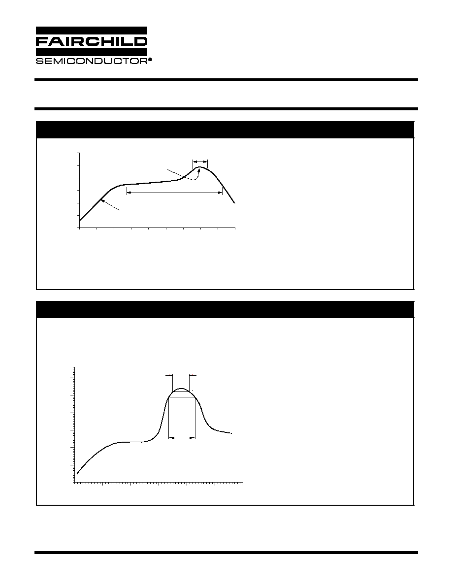
Reflow Profile (FOD070L and FOD073L)
Reflow Profile (FOD270L)
Ramp up = 210
°C/sec
· Peak reflow temperature: 245
°C (package surface temperature)
· Time of temperature higher than 183
°C for 120180 seconds
· One time soldering reflow is recommended
230
° C, 1030 s
Time (Minute)
0
300
250
200
150
100
50
0
0.5
1
1.5
2
2.5
3
3.5
4
4.5
Te
mperature (
°
C)
Time above 183
°C, 120180 sec
245
° C peak
· Peak reflow temperature
260
° C (package surface temperature)
· Time of temperature higher than 245
°C
40 seconds or less
· Number of reflows
Three
300
250
200
Temperature
(
°
C)
150
100
50
50
100
150
200
250
Time (s)
10 s
40 s
260
°
245
°

LIFE SUPPORT POLICY
FAIRCHILD'S PRODUCTS ARE NOT AUTHORIZED FOR USE AS CRITICAL COMPONENTS IN LIFE SUPPORT DEVICES
OR SYSTEMS WITHOUT THE EXPRESS WRITTEN APPROVAL OF THE PRESIDENT OF FAIRCHILD SEMICONDUCTOR
CORPORATION. As used herein:
1. Life support devices or systems are devices or systems
which, (a) are intended for surgical implant into the body, or
(b) support or sustain life, and (c) whose failure to perform
when properly used in accordance with instructions for use
provided in the labeling, can be reasonably expected to
result in a significant injury of the user.
2. A critical component in any component of a life support
device or system whose failure to perform can be
reasonably expected to cause the failure of the life support
device or system, or to affect its safety or effectiveness.
DISCLAIMER
FAIRCHILD SEMICONDUCTOR RESERVES THE RIGHT TO MAKE CHANGES WITHOUT FURTHER NOTICE TO
ANY PRODUCTS HEREIN TO IMPROVE RELIABILITY, FUNCTION OR DESIGN. FAIRCHILD DOES NOT ASSUME
ANY LIABILITY ARISING OUT OF THE APPLICATION OR USE OF ANY PRODUCT OR CIRCUIT DESCRIBED HEREIN;
NEITHER DOES IT CONVEY ANY LICENSE UNDER ITS PATENT RIGHTS, NOR THE RIGHTS OF OTHERS.
8/10/04
Page 17 of 17
© 2004 Fairchild Semiconductor Corporation
LVTTL/LVCMOS COMPATIBLE LOW INPUT
CURRENT HIGH GAIN SPLIT DARLINGTON
OPTOCOUPLERS
SINGLE CHANNEL:
FOD070L
FOD270L
DUAL CHANNEL:
FOD073L