 | ÐлекÑÑоннÑй компоненÑ: FOD617A | СкаÑаÑÑ:  PDF PDF  ZIP ZIP |
Äîêóìåíòàöèÿ è îïèñàíèÿ www.docs.chipfind.ru
©2005 Fairchild Semiconductor Corporation
1
www.fairchildsemi.com
November 2005
FOD814 Series, FOD617 Series, FOD817 Series Rev. 1.0.2
FOD814 Series,
FOD617 Series,
FOD817 Series 4-Pin Phototransistor Optocoupler
s
FOD814 Series, FOD617 Series, FOD817 Series
4-Pin Phototransistor Optocouplers
Features
AC input response (FOD814 only)
Applicable to Pb-free IR reflow soldering
Compact 4-pin package
Current transfer ratio in selected groups:
FOD617A: 4080%
FOD817: 50600%
FOD617B: 63125%
FOD817A:80160%
FOD617C: 100200%
FOD817B: 130260%
FOD617D: 160320%
FOD817C:200400%
FOD814: 20300%
FOD817D:300600%
FOD814A: 50150%
C-UL, UL and VDE approved
High input-output isolation voltage of 5000Vrms
Higher operating temperatures (versus FODXXX
counterparts)
Minimum BV
CEO
of 70V guaranteed
Applications
FOD814 Series
AC line monitor
Unknown polarity DC sensor
Telephone line interface
FOD617 and FOD817 Series
Power supply regulators
Digital logic inputs
Microprocessor inputs
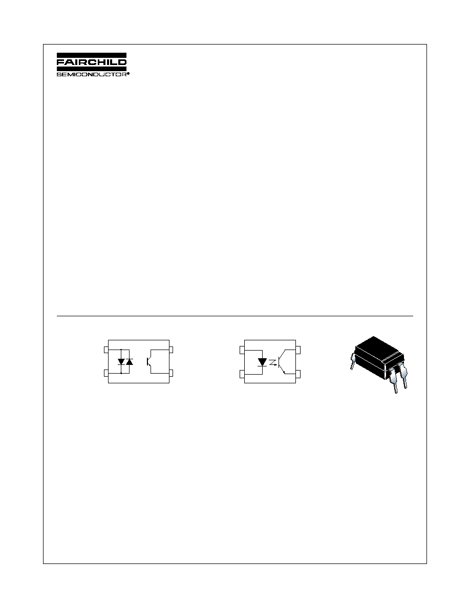
Description
The FOD814 consists of two gallium arsenide infrared
emitting diodes, connected in inverse parallel, driving a
silicon phototransistor output in a 4-pin dual in-line
package. The FOD617/817 Series consists of a gallium
arsenide infrared emitting diode driving a silicon
phototransistor in a 4-pin dual in-line package.
Functional Block Diagram
4
1
1
ANODE, CATHODE
2
4
3
CATHODE, ANODE
COLLECTOR
EMITTER
1
2
4
3 EMITTER
COLLECTOR
ANODE
CATHODE
FOD814
FOD617/817
2
www.fairchildsemi.com
FOD814 Series, FOD617 Series, FOD817 Series Rev. 1.0.2
FOD814 Series,
FOD617 Series,
FOD817 Series 4-Pin Phototransistor Optocoupler
s
Absolute Maximum Ratings
(T
A
= 25°C Unless otherwise specified.)
Parameter
Symbol
Value
Units
FOD814
FOD617/817
TOTAL DEVICE
Storage Temperature
T
STG
-55 to +150
°C
Operating Temperature
T
OPR
-55 to +105
-55 to +110
°C
Lead Solder Temperature
T
SOL
260 for 10 sec
°C
Total Power Dissipation
P
TOT
200
mW
EMITTER
Continuous Forward Current
I
F
±50
50
mA
Reverse Voltage
V
R
--
6
Power Dissipation
Derate above 100°C
P
D
70
1.7
mW
mW/°C
DETECTOR
Collector-Emitter Voltage
V
CEO
70
V
Emitter-Collector Voltage
V
ECO
6
6 (FOD817)
7 (FOD617)
V
Continuous Collector Current
I
C
50
mA
Collector Power Dissipation
Derate above 90°C
P
C
150
2.9
mW
mW/°C
3
www.fairchildsemi.com
FOD814 Series, FOD617 Series, FOD817 Series Rev. 1.0.2
FOD814 Series,
FOD617 Series,
FOD817 Series 4-Pin Phototransistor Optocoupler
s
Electrical/Characteristics
(T
A
= 25°C Unless otherwise specified.)
Individual Component Characteristics
Transfer Characteristics
(T
A
= 25°C Unless otherwise specified.)
*Typical values at T
A
= 25°C
Parameter
Device
Test Conditions
Symbol
Min
Typ*
Max
Unit
EMITTER
Forward Voltage
FOD814
FOD617
FOD817
(I
F
= ±20 mA)
(I
F
= 60 mA)
(I
F
= 20 mA)
V
F
--
--
--
1.2
1.35
1.2
1.4
1.65
1.4
V
Reverse Leakage Current
FOD617
FOD817
(V
R
= 6.0 V)
(V
R
= 4.0 V)
I
R
--
--
0.001
--
10
10
µA
Terminal Capacitance
FOD814
FOD617
FOD817
(V = 0, f = 1 kHz)
(V = 0, f = 1 kHz)
(V = 0, f = 1 kHz)
C
t
--
--
--
50
30
30
250
250
250
pF
DETECTOR
Collector Dark Current
FOD814
FOD617C/
D
FOD617A/
B
FOD817
(V
CE
= 20 V, I
F
= 0)
(V
CE
= 10 V, I
F
= 0)
(V
CE
= 10 V, I
F
= 0)
(V
CE
= 20 V, I
F
= 0)
I
CEO
--
--
--
--
--
1
1
--
100
100
50
100
nA
Collector-Emitter Breakdown
Voltage
FOD814
FOD617
FOD817
(I
C
= 0.1 mA, I
F
= 0)
(I
C
= 100 µA, I
F
= 0)
(I
C
= 0.1 mA, I
F
= 0)
BV
CEO
70
70
70
--
--
--
--
--
--
V
Emitter-Collector Breakdown
Voltage
FOD814
FOD617
FOD817
(I
E
= 10 µA, I
F
= 0)
(I
E
= 10 µA, I
F
= 0)
(I
E
= 10 µA, I
F
= 0)
BV
ECO
6
7
6
--
--
--
--
--
--
V
DC Characteristic
Device
Test Conditions
Symbol
Min
Typ*
Max
Unit
Current Transfer
Ratio
FOD814
I
F
= ±1 mA, V
CE
= 5 V
1
CTR
20
--
300
%
FOD814A
50
150
FOD617A
I
F
= 10 mA, V
CE
= 5 V
1
40
80
FOD617B
63
125
FOD617C
100
200
FOD617D
160
320
FOD617A
I
F
= 1 mA, V
CE
= 5 V
1
13
FOD617B
22
FOD617C
34
FOD617D
56
FOD817
I
F
= 5 mA, V
CE
= 5 V
1
50
--
600
FOD817A
80
--
160
FOD817B
130
--
260
FOD817C
200
--
400
FOD817D
300
--
600
Collector-Emitter
Saturation Voltage
FOD814
I
F
= ±20 mA, I
C
= 1 mA
V
CE (sat)
--
0.1
0.2
V
FOD617
I
F
= 10 mA, I
C
= 2.5 mA
--
--
0.4
FOD817
I
F
= 20 mA, I
C
= 1 mA
--
0.1
0.2
Cut-Off Frequency
FOD814
V
CE
= 5 V, I
C
= 2 mA, R
L
= 100
, -3dB
f
C
15
80
--
KHz
4
www.fairchildsemi.com
FOD814 Series, FOD617 Series, FOD817 Series Rev. 1.0.2
FOD814 Series,
FOD617 Series,
FOD817 Series 4-Pin Phototransistor Optocoupler
s
Transfer Characteristics (continued)
(T
A
= 25°C Unless otherwise specified.)
Isolation Characteristics
*Typical values at T
A
= 25°C
Notes
1. Current Transfer Ratio (CTR) = I
C
/I
F
x 100%.
2.
For test circuit setup and waveforms, refer to page 4.
3. For this test, Pins 1 and 2 are common, and Pins 3 and 4 are common.
AC Characteristic
Device
Test Conditions
Symbol
Min
Typ*
Max
Unit
Response Time (Rise)
FOD814
FOD617
FOD817
V
CE
= 2 V, I
C
= 2 mA, R
L
= 100
2
t
r
--
4
18
µs
Response Time (Fall)
FOD814
FOD617
FOD817
t
f
--
3
18
µs
Characteristic
Device
Test Conditions
Symbol
Min
Typ*
Max
Units
Input-Output Isolation
Voltage
3
FOD814
f = 60Hz, t = 1 min
V
ISO
5000
Vac(rms)
FOD617
FOD817
Isolation Resistance
FOD814
V
I-O
= 500 VDC
R
ISO
5x10
10
1x10
11
--
FOD617
FOD817
Isolation Capacitance
FOD814
V
I-O
= 0, f = 1 MHz
C
ISO
0.6
1.0
pf
FOD617
FOD817
5
www.fairchildsemi.com
FOD814 Series, FOD617 Series, FOD817 Series Rev. 1.0.2
FOD814 Series,
FOD617 Series,
FOD817 Series 4-Pin Phototransistor Optocoupler
s
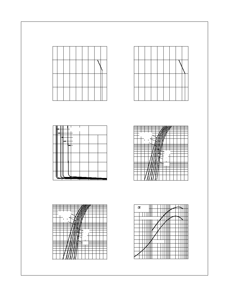
Typical Electrical/Optical Characteristic Curves
(T
A
= 25°C Unless otherwise specified.)
0
1
2
3
4
5
6
COLLECT
OR PO
WER DISSIP
A
TION P
C
(mW)
Fig. 1 Collector Power Dissipation
vs. Ambient Temperature
(FOD814)
FORWARD CURRENT I
F
(mA)
COLLECT
OR-EMITTER SA
TURA
TION
VO
L
T
A
GE V
CE
(sat) (V)
Fig. 3 Collector-Emitter Saturation Voltage
vs. Forward Current
Fig. 5 Forward Current vs. Forward Voltage
(FOD617/817)
FORWARD VOLTAGE V
F
(V)
FOR
W
ARD CURRENT I
F
(mA)
FORWARD CURRENT I
F
(mA)
CURRENT
TRANSFER RA
TIO CTR ( %)
Fig. 6 Current Transfer Ratio
vs. Forward Current
AMBIENT TEMPERATURE T
A
(
°C)
15.0
12.5
10.0
7.5
5.0
2.5
0
V = 5V
Ta= 25
°C
Ic = 0.5m A
1m A
3m A
Ta = 25
°C
7m A
5m A
0
0. 1 0.2
0.5 1
2
5
10 20
50 100
20
40
60
80
100
120
140
-40 -20
0
20
40
60
80 100 120
-55
0
50
100
150
200
COLLECT
OR PO
WER DISSIP
A
TION P
C
(mW)
Fig. 2 Collector Power Dissipation
vs. Ambient Temperature
(FOD617/817)
AMBIENT TEMPERATURE T
A
(
°C)
-40 -20
0
20
40
60
80 100 120
-55
0
50
100
150
200
0.5
1.0
1.5
2.0
T
A
= 110
o
C
75
o
C
50
o
C
25
o
C
0
o
C
-30
o
C
-55
o
C
0.1
1
10
100
FOD814
FOD617/817
Fig. 4 Forward Current vs. Forward Voltage
(FOD814)
FORWARD VOLTAGE V
F
(V)
FOR
W
ARD CURRENT I
F
(mA)
0.5
1.0
1.5
2.0
T
A
= 105
o
C
75
o
C
50
o
C
25
o
C
0
o
C
-30
o
C
-55
o
C
0.1
1
10
100