 | –≠–ª–µ–∫—Ç—Ä–æ–Ω–Ω—ã–π –∫–æ–º–ø–æ–Ω–µ–Ω—Ç: FQI45N03L | –°–∫–∞—á–∞—Ç—å:  PDF PDF  ZIP ZIP |
May 2001
QFET
TM
FQB45N03
L
/
FQI
45N03L
©2001 Fairchild Semiconductor Corporation
Rev. A1. May 2001
FQB45N03L / FQI45N03L
30V LOGIC N-Channel MOSFET
General Description
These N-Channel enhancement mode power field effect
transistors are produced using Fairchild's proprietary,
planar stripe, DMOS technology.
This advanced technology has been especially tailored to
minimize on-state resistance, provide superior switching
performance, and withstand high energy pulse in the
avalanche and commutation mode. These devices are well
suited for low voltage applications such as DC/DC
converters, high efficiency switching for power
management in portable and battery operated products.
Features
∑ 45A, 30V, R
DS(on)
= 0.018
@V
GS
= 10 V
∑ Low gate charge ( typical 15 nC)
∑ Low Crss ( typical 105 pF)
∑ Fast switching
∑ 100% avalanche tested
∑ Improved dv/dt capability
∑ 175
∞
C maximum junction temperature rating
! "
!
!
!
"
"
"
! "
!
!
!
"
"
"
Absolute Maximum Ratings
T
C
= 25∞C unless otherwise noted
Thermal Characteristics
Symbol
Parameter
FQB45N03L / FQI45N03L
Units
V
DSS
Drain-Source Voltage
30
V
I
D
Drain Current
- Continuous (T
C
= 25∞C)
45
A
- Continuous (T
C
= 100∞C)
31.8
A
I
DM
Drain Current
- Pulsed
(Note 1)
180
A
V
GSS
Gate-Source Voltage
±
20
V
E
AS
Single Pulsed Avalanche Energy
(Note 2)
200
mJ
I
AR
Avalanche Current
(Note 1)
45
A
E
AR
Repetitive Avalanche Energy
(Note 1)
7.5
mJ
dv/dt
Peak Diode Recovery dv/dt
(Note 3)
7.0
V/ns
P
D
Power Dissipation (T
A
= 25∞C) *
3.75
W
Power Dissipation (T
C
= 25∞C)
75
W
- Derate above 25∞C
0.5
W/∞C
T
J
, T
STG
Operating and Storage Temperature Range
-55 to +175
∞C
T
L
Maximum lead temperature for soldering purposes,
1/8" from case for 5 seconds
300
∞C
Symbol
Parameter
Typ
Max
Units
R
JC
Thermal Resistance, Junction-to-Case
--
2.0
∞C
/
W
R
JA
Thermal Resistance, Junction-to-Ambient *
--
40
∞C
/
W
R
JA
Thermal Resistance, Junction-to-Ambient
--
62.5
∞C
/
W
* When mounted on the minimum pad size recommended (PCB Mount)
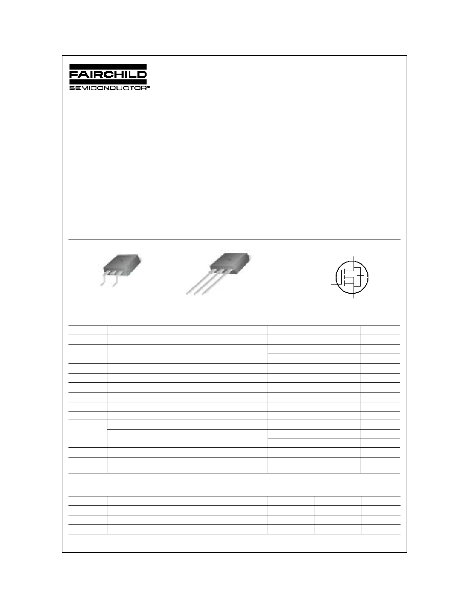
S
D
G
D
2
-PAK
FQB Series
I
2
-PAK
FQI Series
G
S
D
G
S
D
FQB45N03
L
/
FQI
45N03L
Rev. A1. May 2001
©2001 Fairchild Semiconductor Corporation
Electrical Characteristics
T
C
= 25∞C unless otherwise noted
Notes:
1. Repetitive Rating : Pulse width limited by maximum junction temperature
2. L = 98
µ
H, I
AS
= 45A, V
DD
= 15V, R
G
= 25
,
Starting T
J
= 25∞C
3. I
SD
45A, di/dt
300A/us, V
DD
BV
DSS,
Starting T
J
= 25∞C
4. Pulse Test : Pulse width
300
µ
s, Duty cycle
2%
5. Essentially independent of operating temperature
Symbol
Parameter
Test Conditions
Min
Typ
Max
Units
Off Characteristics
BV
DSS
Drain-Source Breakdown Voltage
V
GS
= 0 V, I
D
= 250
µ
A
30
--
--
V
BV
DSS
/
T
J
Breakdown Voltage Temperature
Coefficient
I
D
= 250
µ
A, Referenced to
25∞C
--
0.03
--
V/∞C
I
DSS
Zero Gate Voltage Drain Current
V
DS
= 30 V, V
GS
= 0 V
--
--
1
µ
A
V
DS
= 24 V, T
C
= 150∞C
--
--
10
µ
A
I
GSSF
Gate-Body Leakage Current, Forward
V
GS
= 20 V, V
DS
= 0 V
--
--
100
nA
I
GSSR
Gate-Body Leakage Current, Reverse
V
GS
= -20 V, V
DS
= 0 V
--
--
-100
nA
On Characteristics
V
GS(th)
Gate Threshold Voltage
V
DS
= V
GS
, I
D
= 250
µ
A
1.0
--
2.5
V
R
DS(on)
Static Drain-Source
On-Resistance
V
GS
= 10 V, I
D
= 22.5 A
V
GS
= 5 V, I
D
= 22.5 A
--
--
0.0136
0.0192
0.018
0.025
g
FS
Forward Transconductance
V
DS
= 15 V, I
D
= 22.5 A
--
24.3
--
S
Dynamic Characteristics
C
iss
Input Capacitance
V
DS
= 25 V, V
GS
= 0 V,
f = 1.0 MHz
--
780
1000
pF
C
oss
Output Capacitance
--
420
550
pF
C
rss
Reverse Transfer Capacitance
--
105
140
pF
Switching Characteristics
t
d(on)
Turn-On Delay Time
V
DD
= 15 V, I
D
= 22.5 A,
R
G
= 25
--
15
40
ns
t
r
Turn-On Rise Time
--
130
270
ns
t
d(off)
Turn-Off Delay Time
--
7.5
25
ns
t
f
Turn-Off Fall Time
--
60
130
ns
Q
g
Total Gate Charge
V
DS
= 24 V, I
D
= 45 A,
V
GS
= 5 V
--
15
20
nC
Q
gs
Gate-Source Charge
--
5.0
--
nC
Q
gd
Gate-Drain Charge
--
8.0
--
nC
Drain-Source Diode Characteristics and Maximum Ratings
I
S
Maximum Continuous Drain-Source Diode Forward Current
--
--
45
A
I
SM
Maximum Pulsed Drain-Source Diode Forward Current
--
--
180
A
V
SD
Drain-Source Diode Forward Voltage
V
GS
= 0 V, I
S
= 45 A
--
--
1.5
V
t
rr
Reverse Recovery Time
V
GS
= 0 V, I
S
= 45 A,
dI
F
/ dt = 100 A/
µ
s
--
35
--
ns
Q
rr
Reverse Recovery Charge
--
30
--
nC
(Note 4)
(Note 4, 5)
(Note 4, 5)
(Note 4)
FQB45N03
L
/
FQI
45N03L
©2001 Fairchild Semiconductor Corporation
Rev. A1. May 2001
0.2
0.4
0.6
0.8
1.0
1.2
1.4
1.6
1.8
10
-1
10
0
10
1
10
2
175
Notes :
1. V
GS
= 0V
2. 250
s Pulse Test
25
I
DR
,
Re
v
e
r
s
e
Dr
a
i
n
Cu
r
r
e
n
t
[
A
]
V
SD
, Source-Drain voltage [V]
0
50
100
150
200
250
300
0
10
20
30
40
50
V
GS
= 5V
V
GS
= 10V
Note : T
J
= 25
R
DS
(
O
N)
[m
],
D
r
ai
n-
S
our
ce
O
n
-
R
e
s
i
s
t
a
n
c
e
I
D
, Drain Current [A]
0
2
4
6
8
10
10
-1
10
0
10
1
10
2
175
25
-55
Notes :
1. V
DS
= 15V
2. 250
s Pulse Test
I
D
, D
r
a
i
n
C
u
r
r
e
n
t [A
]
V
GS
, Gate-Source Voltage [V]
10
-1
10
0
10
1
10
1
10
2
V
GS
Top : 10.0 V
8.0 V
6.0 V
5.0 V
4.5 V
4.0 V
3.5 V
Bottom : 3.0 V
Notes :
1. 250
s Pulse Test
2. T
C
= 25
I
D
,
D
r
ai
n
C
u
r
r
e
n
t
[
A
]
V
DS
, Drain-Source Voltage [V]
0
5
10
15
20
25
30
0
2
4
6
8
10
12
V
DS
= 15V
V
DS
= 24V
Note : I
D
= 45A
V
GS
,
G
a
t
e
-
S
ou
r
c
e V
o
l
t
a
g
e
[
V
]
Q
G
, Total Gate Charge [nC]
10
-1
10
0
10
1
0
500
1000
1500
2000
2500
C
iss
= C
gs
+ C
gd
(C
ds
= shorted)
C
oss
= C
ds
+ C
gd
C
rss
= C
gd
Notes :
1. V
GS
= 0 V
2. f = 1 MHz
C
rss
C
oss
C
iss
C
apa
ci
t
anc
e [
p
F]
V
DS
, Drain-Source Voltage [V]
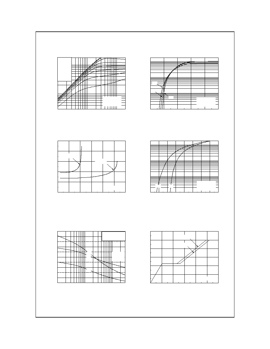
Typical Characteristics
Figure 5. Capacitance Characteristics
Figure 6. Gate Charge Characteristics
Figure 3. On-Resistance Variation vs.
Drain Current and Gate Voltage
Figure 4. Body Diode Forward Voltage
Variation vs. Source Current
and Temperature
Figure 2. Transfer Characteristics
Figure 1. On-Region Characteristics
FQB45N03
L
/
FQI
45N03L
©2001 Fairchild Semiconductor Corporation
Rev. A1. May 2001
1 0
-5
1 0
-4
1 0
-3
1 0
-2
1 0
-1
1 0
0
1 0
1
1 0
-2
1 0
-1
1 0
0
N o te s :
1 . Z
J C
( t) = 2 .0
/W M a x .
2 . D u ty F a c to r , D = t
1
/t
2
3 . T
J M
- T
C
= P
D M
* Z
J C
( t)
s in g le p u ls e
D = 0 .5
0 .0 2
0 .2
0 .0 5
0 .1
0 .0 1
Z
JC
(
t
)
,
T
her
m
a
l
R
e
s
p
on
s
e
t
1
, S q u a r e W a v e P u ls e D u r a t io n [ s e c ]
25
50
75
100
125
150
175
0
10
20
30
40
50
I
D
,
D
r
ai
n
C
u
r
r
e
nt
[
A
]
T
C
, Case Temperature [
]
10
-1
10
0
10
1
10
0
10
1
10
2
DC
10 ms
1 ms
100
µ
s
Operation in This Area
is Limited by R
DS(on)
Notes :
1. T
C
= 25
o
C
2. T
J
= 175
o
C
3. Single Pulse
I
D
,
D
r
ai
n
C
u
r
r
e
nt
[
A
]
V
DS
, Drain-Source Voltage [V]
-100
-50
0
50
100
150
200
0.0
0.5
1.0
1.5
2.0
2.5
Notes :
1. V
GS
= 10 V
2. I
D
= 22.5 A
R
DS
(
O
N)
,
(
N
or
m
a
l
i
z
e
d)
D
r
ai
n-
S
o
ur
c
e
O
n
-
R
es
i
s
t
a
nc
e
T
J
, Junction Temperature [
o
C]
-100
-50
0
50
100
150
200
0.8
0.9
1.0
1.1
1.2
Notes :
1. V
GS
= 0 V
2. I
D
= 250
A
BV
DSS
, (
N
o
r
m
a
liz
e
d
)
D
r
ai
n-
S
o
u
r
ce B
r
eak
d
o
w
n
V
o
l
t
age
T
J
, Junction Temperature [
o
C]
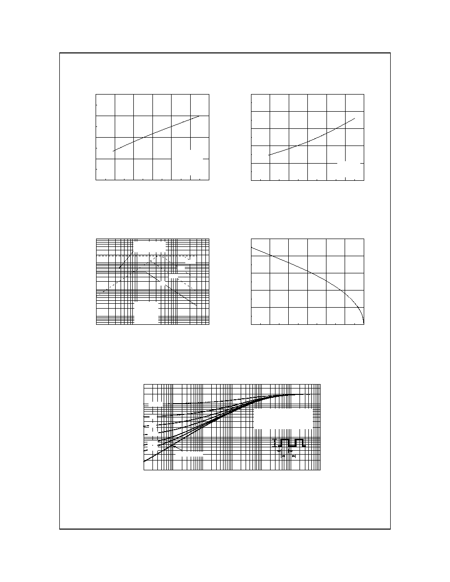
Typical Characteristics
(Continued)
Figure 9. Maximum Safe Operating Area
Figure 10. Maximum Drain Current
vs. Case Temperature
Figure 7. Breakdown Voltage Variation
vs. Temperature
Figure 8. On-Resistance Variation
vs. Temperature
Figure 11. Transient Thermal Response Curve
t
1
P
DM
t
2
FQB45N03
L
/
FQI
45N03L
©2001 Fairchild Semiconductor Corporation
Rev. A1. May 2001
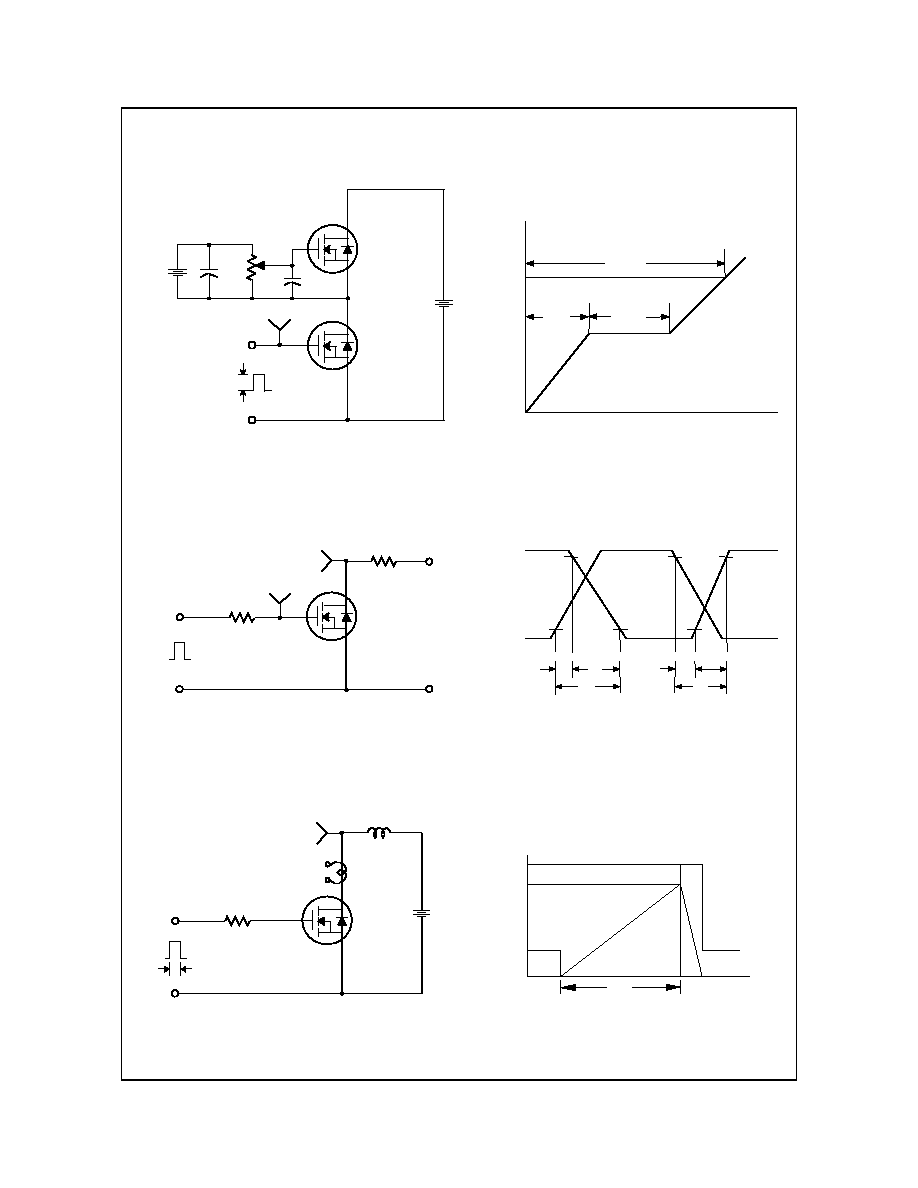
Charge
V
GS
5V
Q
g
Q
gs
Q
gd
3mA
V
GS
DUT
V
DS
300nF
50K
200nF
12V
Same Type
as DUT
Charge
V
GS
5V
Q
g
Q
gs
Q
gd
3mA
V
GS
DUT
V
DS
300nF
50K
200nF
12V
Same Type
as DUT
V
GS
V
DS
10%
90%
t
d(on)
t
r
t
on
t
off
t
d(off)
t
f
V
DD
5V
V
DS
R
L
DUT
R
G
V
GS
V
GS
V
DS
10%
90%
t
d(on)
t
r
t
on
t
off
t
d(off)
t
f
V
DD
5V
V
DS
R
L
DUT
R
G
V
GS
E
AS
=
L I
AS
2
----
2
1
--------------------
BV
DSS
- V
DD
BV
DSS
V
DD
V
DS
BV
DSS
t
p
V
DD
I
AS
V
DS
(t)
I
D
(t)
Time
10V
DUT
R
G
L
I
D
t
p
E
AS
=
L I
AS
2
----
2
1
E
AS
=
L I
AS
2
----
2
1
----
2
1
--------------------
BV
DSS
- V
DD
BV
DSS
V
DD
V
DS
BV
DSS
t
p
V
DD
I
AS
V
DS
(t)
I
D
(t)
Time
10V
DUT
R
G
L
L
I
D
I
D
t
p
Gate Charge Test Circuit & Waveform
Resistive Switching Test Circuit & Waveforms
Unclamped Inductive Switching Test Circuit & Waveforms