 | –≠–ª–µ–∫—Ç—Ä–æ–Ω–Ω—ã–π –∫–æ–º–ø–æ–Ω–µ–Ω—Ç: FQP1P50 | –°–∫–∞—á–∞—Ç—å:  PDF PDF  ZIP ZIP |
©2000 Fairchild Semiconductor International
June 2000
Rev. A, June 2000
FQ
P1P5
0
QFET
QFET
QFET
QFET
TM
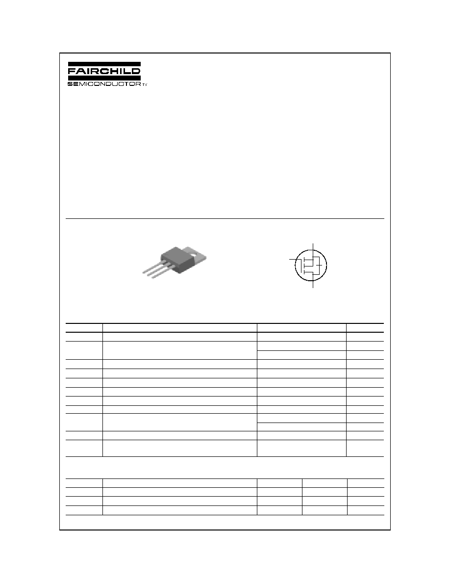
FQP1P50
500V P-Channel MOSFET
General Description
These P-Channel enhancement mode power field effect
transistors are produced using Fairchild's proprietary,
planar stripe, DMOS technology.
This advanced technology has been especially tailored to
minimize on-state resistance, provide superior switching
performance, and withstand high energy pulse in the
avalanche and commutation mode. These devices are well
suited for electronic lamp ballast based on compl
ementary
half bridge.
Features
∑ -1.5A, -500V, R
DS(on)
= 10.5
@V
GS
= -10 V
∑ Low gate charge ( typical 11 nC)
∑ Low Crss ( typical 6.0 pF)
∑ Fast switching
∑ 100% avalanche tested
∑ Improved dv/dt capability
Absolute Maximum Ratings
T
C
= 25∞C unless otherwise noted
Thermal Characteristics
Symbol
Parameter
FQP1P50
Units
V
DSS
Drain-Source Voltage
-500
V
I
D
Drain Current
- Continuous (T
C
= 25∞C)
-1.5
A
- Continuous (T
C
= 100∞C)
-0.95
A
I
DM
Drain Current
- Pulsed
(Note 1)
-6.0
A
V
GSS
Gate-Source Voltage
±
30
V
E
AS
Single Pulsed Avalanche Energy
(Note 2)
110
mJ
I
AR
Avalanche Current
(Note 1)
-1.5
A
E
AR
Repetitive Avalanche Energy
(Note 1)
6.3
mJ
dv/dt
Peak Diode Recovery dv/dt
(Note 3)
-4.5
V/ns
P
D
Power Dissipation (T
C
= 25∞C)
63
W
- Derate above 25∞C
0.51
W/∞C
T
J
, T
STG
Operating and Storage Temperature Range
-55 to +150
∞C
T
L
Maximum lead temperature for soldering purposes,
1/8
"
from case for 5 seconds
300
∞C
Symbol
Parameter
Typ
Max
Units
R
JC
Thermal Resistance, Junction-to-Case
--
1.98
∞C
/
W
R
CS
Thermal Resistance, Case-to-Sink
0.5
--
∞C
/
W
R
JA
Thermal Resistance, Junction-to-Ambient
--
62.5
∞C
/
W
TO-220
FQP Series
G
S
D
!
!
!
!
!
!
!
!
!
!
!
!
!
!
!
!
!
!
!
!
!
!
!
!
S
D
G
©2000 Fairchild Semiconductor International
FQ
P1P50
(Note 4)
(Note 4, 5)
(Note 4, 5)
(Note 4)
Rev. A, June 2000
Elerical Characteristics
T
C
= 25∞C unless otherwise noted
Notes:
1. Repetitive Rating : Pulse width limited by maximum junction temperature
2. L = 88mH, I
AS
= -1.5A, V
DD
= -50V, R
G
= 25
,
Starting T
J
= 25∞C
3. I
SD
-1.5A, di/dt
200A/
µ
s, V
DD
BV
DSS,
Starting T
J
= 25∞C
4. Pulse Test : Pulse width
300
µ
s, Duty cycle
2%
5. Essentially independent of operating temperature
Symbol
Parameter
Test Conditions
Min
Typ
Max
Units
Off Characteristics
BV
DSS
Drain-Source Breakdown Voltage
V
GS
= 0 V, I
D
= -250
µ
A
-500
--
--
V
BV
DSS
/
T
J
Breakdown Voltage Temperature
Coefficient
I
D
= -250
µ
A, Referenced to 25∞C
--
-
--
V/∞C
I
DSS
Zero Gate Voltage Drain Current
V
DS
= -500 V, V
GS
= 0 V
--
--
-1
µ
A
V
DS
= -400 V, T
C
= 125∞C
--
--
-10
µ
A
I
GSSF
Gate-Body Leakage Current, Forward
V
GS
= -30 V, V
DS
= 0 V
--
--
-100
nA
I
GSSR
Gate-Body Leakage Current, Reverse
V
GS
= 30 V, V
DS
= 0 V
--
--
100
nA
On Characteristics
V
GS(th)
Gate Threshold Voltage
V
DS
= V
GS
, I
D
= -250
µ
A
-3.0
--
-5.0
V
R
DS(on)
Static Drain-Source
On-Resistance
V
GS
= -10 V, I
D
= -0.75 A
--
8.0
10.5
g
FS
Forward Transconductance
V
DS
= -50 V, I
D
= -0.75 A
--
1.26
--
S
Dynamic Characteristics
C
iss
Input Capacitance
V
DS
= -25 V, V
GS
= 0 V,
f = 1.0 MHz
--
270
350
pF
C
oss
Output Capacitance
--
40
50
pF
C
rss
Reverse Transfer Capacitance
--
6.0
8.0
pF
Switching Characteristics
t
d(on)
Turn-On Delay Time
V
DD
= -250 V, I
D
= -1.5 A,
R
G
= 25
--
9.0
30
ns
t
r
Turn-On Rise Time
--
25
60
ns
t
d(off)
Turn-Off Delay Time
--
27
65
ns
t
f
Turn-Off Fall Time
--
30
70
ns
Q
g
Total Gate Charge
V
DS
= -400 V, I
D
= -1.5 A,
V
GS
= -10 V
--
11
14
nC
Q
gs
Gate-Source Charge
--
2.0
--
nC
Q
gd
Gate-Drain Charge
--
5.6
--
nC
Drain-Source Diode Characteristics and Maximum Ratings
I
S
Maximum Continuous Drain-Source Diode Forward Current
--
--
-1.5
A
I
SM
Maximum Pulsed Drain-Source Diode Forward Current
--
--
-6.0
A
V
SD
Drain-Source Diode Forward Voltage
V
GS
= 0 V, I
S
= -1.5 A
--
--
-5.0
V
t
rr
Reverse Recovery Time
V
GS
= 0 V, I
S
= -1.5 A,
dI
F
/ dt = 100 A/
µ
s
--
200
--
ns
Q
rr
Reverse Recovery Charge
--
0.7
--
µ
C
©2000 Fairchild Semiconductor International
FQ
P1P5
0
Rev. A, June 2000
0
2
4
6
8
10
12
0
2
4
6
8
10
12
V
DS
= -250V
V
DS
= -100V
V
DS
= -400V
Note : I
D
= -1.5 A
-V
GS
,
G
a
t
e
-
S
our
c
e
V
o
l
t
ag
e [
V
]
Q
G
, Total Gate Charge [nC]
10
-1
10
0
10
1
0
100
200
300
400
500
600
C
iss
= C
gs
+ C
gd
(C
ds
= shorted)
C
oss
= C
ds
+ C
gd
C
rss
= C
gd
Notes :
1. V
GS
= 0 V
2. f = 1 MHz
C
rss
C
oss
C
iss
C
a
pac
i
t
a
n
c
e
[
p
F]
V
DS
, Drain-Source Voltage [V]
0.0
0.5
1.0
1.5
2.0
2.5
3.0
10
-1
10
0
150
Notes :
1. V
GS
= 0V
2. 250
s Pulse Test
25
-I
DR
,
Re
v
e
r
s
e
Dr
a
i
n
Cu
r
r
e
n
t
[
A
]
-V
SD
, Source-Drain Voltage [V]
0
1
2
3
4
6
8
10
12
14
16
Note : T
J
= 25
V
GS
= - 20V
V
GS
= - 10V
R
D
S
(
on)
[
],
D
r
ai
n
-
S
o
u
r
ce
O
n
-
R
esi
s
t
a
nce
-I
D
, Drain Current [A]
2
4
6
8
10
10
-1
10
0
150
25
-55
Notes :
1. V
DS
= -50V
2. 250
s Pulse Test
-I
D
,
D
r
ai
n
C
u
r
r
ent
[
A
]
-V
GS
, Gate-Source Voltage [V]
10
-1
10
0
10
1
10
-2
10
-1
10
0
V
GS
Top : -15.0 V
-10.0 V
-8.0 V
-7.0 V
-6.5 V
-6.0 V
Bottom : -5.5 V
Notes :
1. 250
s Pulse Test
2. T
C
= 25
-I
D
,
D
r
ai
n
C
u
r
r
ent
[
A
]
-V
DS
, Drain-Source Voltage [V]
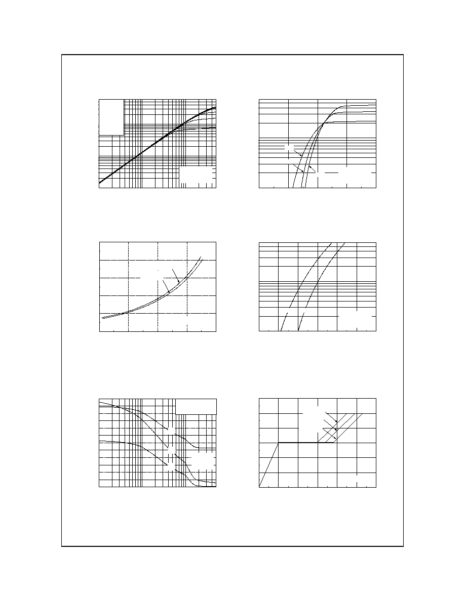
Typical Characteristics
Figure 5. Capacitance Characteristics
Figure 6. Gate Charge Characteristics
Figure 3. On-Resistance Variation vs.
Drain Current and Gate Voltage
Figure 4. Body Diode Forward Voltage
Variation vs. Source Current
and Temperature
Figure 2. Transfer Characteristics
Figure 1. On-Region Characteristics
©2000 Fairchild Semiconductor International
FQ
P1P50
Rev. A, June 2000
25
50
75
100
125
150
0.0
0.3
0.6
0.9
1.2
1.5
-I
D
,
Dr
a
i
n
Cu
r
r
e
n
t
[
A
]
T
C
, Case Temperature [
]
10
0
10
1
10
2
10
3
10
-2
10
-1
10
0
10
1
DC
10 ms
1 ms
100
µ
s
Operation in This Area
is Limited by R
DS(on)
Notes :
1. T
C
= 25
o
C
2. T
J
= 150
o
C
3. Single Pulse
-I
D
, D
r
a
i
n
C
u
r
r
e
n
t [A
]
-V
DS
, Drain-Source Voltage [V]
-100
-50
0
50
100
150
200
0.0
0.5
1.0
1.5
2.0
2.5
Notes :
1. V
GS
= -10 V
2. I
D
= -0.75 A
R
DS
(
O
N
)
, (
N
o
r
m
a
liz
e
d
)
D
r
ai
n
-
S
o
u
r
c
e
O
n
-
R
es
i
s
t
a
nc
e
T
J
, Junction Temperature [
o
C]
-100
-50
0
50
100
150
200
0.8
0.9
1.0
1.1
1.2
Notes :
1. V
GS
= 0 V
2. I
D
= -250
A
-B
V
DSS
,
(
N
or
m
a
l
i
z
ed)
D
r
ai
n-
S
our
c
e
B
r
eak
do
w
n
V
o
l
t
a
g
e
T
J
, Junction Temperature [
o
C]
1 0
-5
1 0
-4
1 0
-3
1 0
-2
1 0
-1
1 0
0
1 0
1
1 0
-2
1 0
-1
1 0
0
N o te s :
1 . Z
J C
( t) = 1 .9 8
/W M a x .
2 . D u ty F a c t o r , D = t
1
/t
2
3 . T
J M
- T
C
= P
D M
* Z
J C
( t)
s in g le p u ls e
D = 0 .5
0 .0 2
0 .2
0 .0 5
0 .1
0 .0 1
Z
JC
(t
),
T
h
e
r
m
a
l
R
e
s
p
o
n
s
e
t
1
, S q u a r e W a v e P u ls e D u r a t io n [ s e c ]
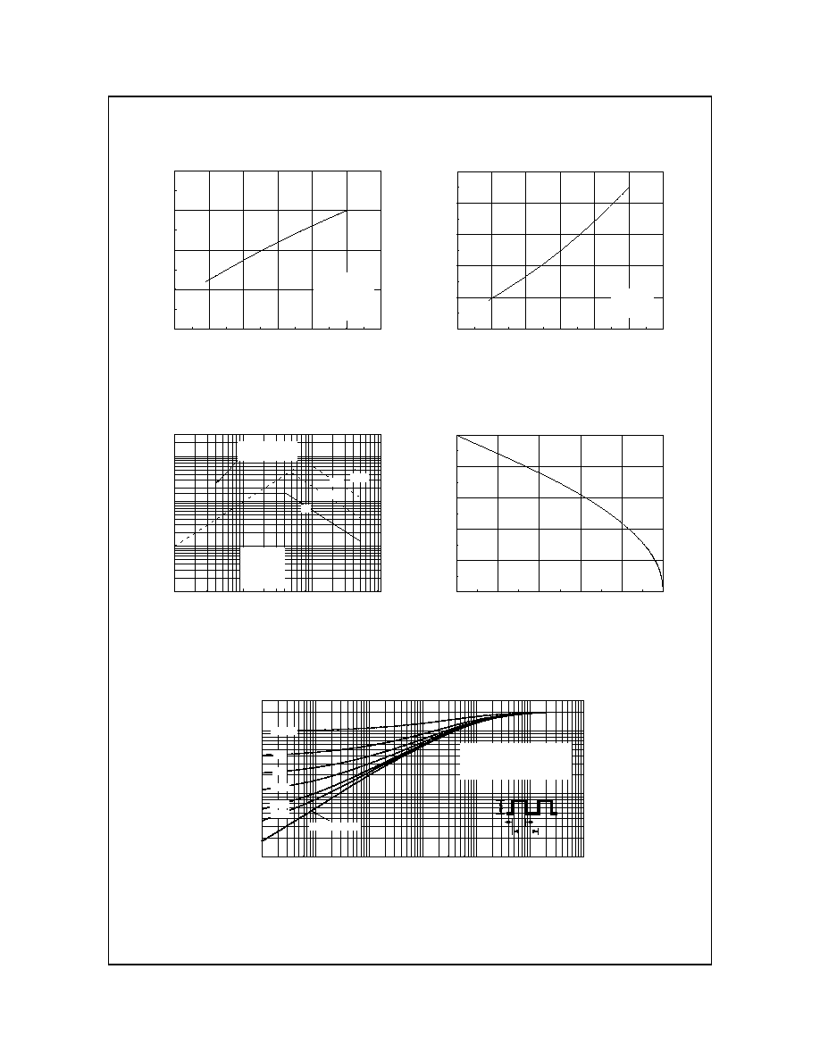
Typical Characteristics
(Continued)
Figure 9. Maximum Safe Operating Area
Figure 10. Maximum Drain Current
vs. Case Temperature
Figure 7. Breakdown Voltage Variation
vs. Temperature
Figure 8. On-Resistance Variation
vs. Temperature
Figure 11. Transient Thermal Response Curve
t
1
P
DM
t
2
©2000 Fairchild Semiconductor International
FQ
P1P5
0
Rev. A, June 2000
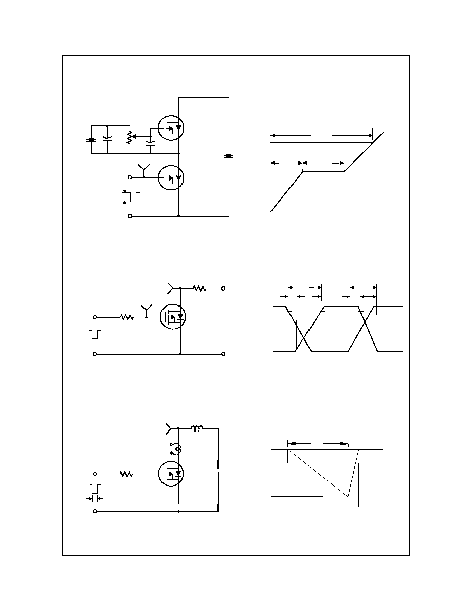
Charge
V
GS
-10V
Q
g
Q
gs
Q
gd
-3mA
V
GS
DUT
V
DS
300nF
50K
200nF
12V
Same Type
as DUT
Charge
V
GS
-10V
Q
g
Q
gs
Q
gd
-3mA
V
GS
DUT
V
DS
300nF
50K
200nF
12V
Same Type
as DUT
V
DS
V
GS
10%
90%
t
d(on)
t
r
t
on
t
off
t
d(off)
t
f
V
DD
-10V
V
DS
R
L
DUT
R
G
V
GS
V
DS
V
GS
10%
90%
t
d(on)
t
r
t
on
t
off
t
d(off)
t
f
V
DD
-10V
V
DS
R
L
DUT
R
G
V
GS
E
AS
=
L I
AS
2
----
2
1
--------------------
BV
DSS
- V
DD
BV
DSS
V
DD
V
DS
BV
DSS
t
p
V
DD
I
AS
V
DS
(t)
I
D
(t)
Time
-10V
DUT
R
G
L
I
D
t
p
E
AS
=
L I
AS
2
----
2
1
E
AS
=
L I
AS
2
----
2
1
----
2
1
--------------------
BV
DSS
- V
DD
BV
DSS
V
DD
V
DS
BV
DSS
t
p
V
DD
I
AS
V
DS
(t)
I
D
(t)
Time
-10V
DUT
R
G
L
L
I
D
I
D
t
p
Gate Charge Test Circuit & Waveform
Resistive Switching Test Circuit & Waveforms
Unclamped Inductive Switching Test Circuit & Waveforms