 | –≠–ª–µ–∫—Ç—Ä–æ–Ω–Ω—ã–π –∫–æ–º–ø–æ–Ω–µ–Ω—Ç: FQS4900 | –°–∫–∞—á–∞—Ç—å:  PDF PDF  ZIP ZIP |
©2000 Fairchild Semiconductor International
August 2000
Rev. A, August 2000
FQS490
0
QFET
QFET
QFET
QFET
TM
FQS4900
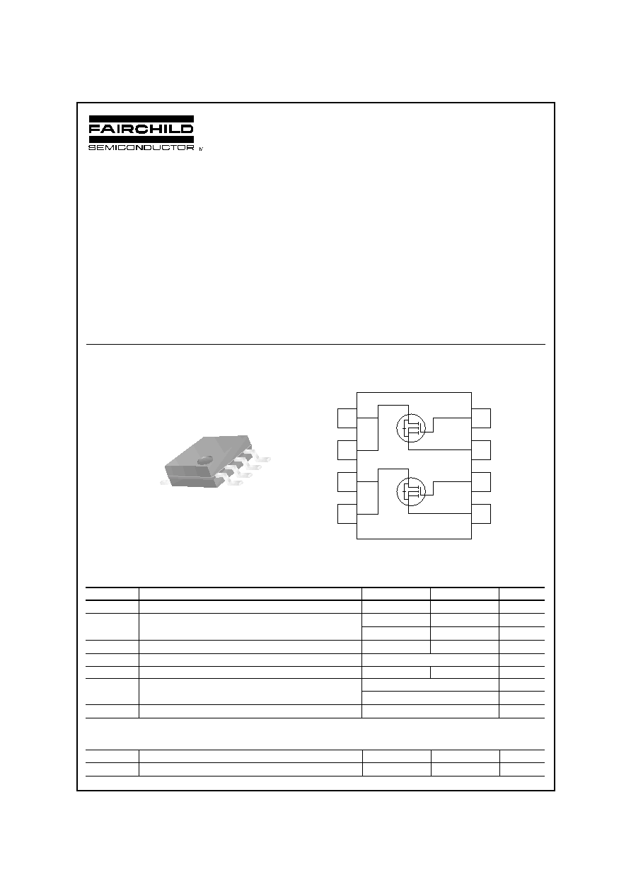
Dual N & P-Channel, Logic Level MOSFET
General Description
These dual N and P-channel enhancement mode power
field effect transistors are produced using Fairchild's
proprietary, planar stripe, DMOS technology.
This advanced technology has been especially tailored to
minimize on-state resistance, provide superior switching
performance, and withstand high energy pulse in the
avalanche and commutation mode. This device is well
suited for high interface in telephone sets.
Features
∑ N-Channel 1.3A, 60V, R
DS(on)
= 0.55
@ V
GS
= 10 V
R
DS(on)
= 0.65
@ V
GS
= 5 V
P-Channel -0.3A, -300V, R
DS(on)
= 15.5
@ V
GS
= -10 V
R
DS(on)
= 16
@ V
GS
=- 5 V
∑ Low gate charge ( typical N-Channel 1.6 nC)
( typical P-Channel 3.6 nC)
∑ Fast switching
∑ Improved dv/dt capability
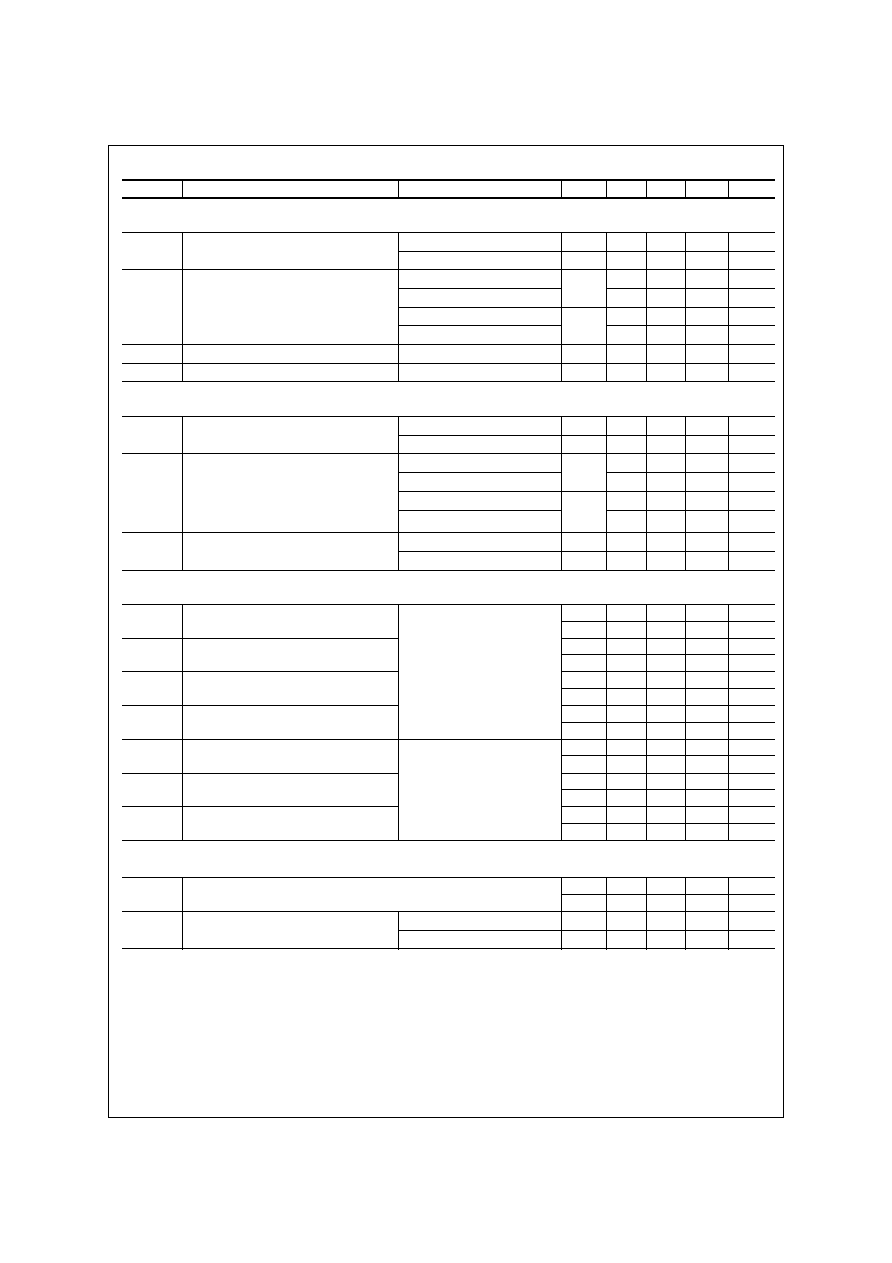
Absolute Maximum Ratings
T
A
= 25∞C unless otherwise noted
Thermal Characteristics
Symbol
Parameter
N-Channel
P-Channel
Units
V
DSS
Drain-Source Voltage
60
-300
V
I
D
Drain Current
- Continuous (T
A
= 25∞C)
1.3
-0.3
A
- Continuous (T
A
= 70∞C)
0.82
-0.19
A
I
DM
Drain Curent
- Pulsed
(Note 1)
5.2
-1.2
A
V
GSS
Gate-Source Voltage
±
20
V
dv/dt
Peak Diode Recovery dv/dt
(Note 2)
7.0
4.5
V/ns
P
D
Power Dissipation (T
A
= 25∞C)
2.0
W
(T
A
= 70∞C)
1.3
W
T
J
, T
STG
Operating and Storage Temperature Range
-55 to +150
∞C
Symbol
Parameter
Typ
Max
Units
R
JA
Thermal Resistance, Junction-to-Ambient
--
62.5
∞C
/
W
!
"
!
!
!
!
#
$
!
!
!
!
!
"
!
!
!
!
#
$
!
!
!
!
4
3
2
1
5
6
7
8
S1
G1
S2
G2
D1
D1
D2
D2
©2000 Fairchild Semiconductor International
FQS
4900
Rev. A, August 2000
Electrical Characteristics
T
A
= 25∞C unless otherwise noted
Notes:
1. Repetitive Rating : Pulse width limited by maximum junction temperature
3. Pulse Test : Pulse width
300
µ
s, Duty cycle
2%
4. Essentially independent of operating temperature
Symbol
Parameter
Test Conditions
Type
Min
Typ
Max
Units
Off Characteristics
BV
DSS
Drain-Source Breakdown Voltage
V
GS
= 0 V, I
D
= 250
µ
A
N-Ch
60
--
--
V
V
GS
= 0 V, I
D
= -250
µ
A
P-Ch
-300
--
--
V
I
DSS
Zero Gate Voltage Drain Current
V
DS
= 60 V, V
GS
= 0 V
N-Ch
--
--
1
µ
A
V
DS
= 48 V, T
C
= 55∞C
--
--
10
µ
A
V
DS
= -300 V, V
GS
= 0 V
P-Ch
--
--
-1
µ
A
V
DS
= -240 V, T
C
= 55∞C
--
--
-10
µ
A
I
GSSF
Gate-Body Leakage Current, Forward
V
GS
= 20 V, V
DS
= 0 V
All
--
--
100
nA
I
GSSR
Gate-Body Leakage Current, Reverse
V
GS
= -20 V, V
DS
= 0 V
All
--
--
-100
nA
On Characteristics
V
GS(th)
Gate Threshold Voltage
V
DS
= 4V, I
D
= 20 mA
N-Ch
1.0
--
1.95
V
V
DS
= 4V, I
D
= -20 mA
P-Ch
-1.0
--
-1.95
V
R
DS(on)
Static Drain-Source On-Resistance
V
GS
= 10 V, I
D
= 0.65 A
N-Ch
--
0.39
0.55
V
GS
= 5 V, I
D
= 0.65 A
--
0.46
0.65
V
GS
= -10 V, I
D
= -0.15 A
P-CH
--
11.2
15.5
V
GS
= -5 V, I
D
= -0.15 A
--
11.4
16
g
FS
Forward Transconductance
V
DS
= 10 V, I
D
= 0.65 A
N-CH
--
1.7
--
S
V
DS
= -10 V, I
D
= -0.15 A
P-CH
--
0.6
--
S
Switching Characteristics
t
d(on)
Turn-On Delay Time
N-Channel
V
DD
= 30 V, I
D
= 1.3 A,
R
G
= 25
P-Channel
V
DD
= -150 V, I
D
= -0.3 A,
R
G
= 25
N-Ch
--
5.7
21
ns
P-Ch
--
10
30
ns
t
r
Turn-On Rise Time
N-Ch
--
21
50
ns
P-Ch
--
25
60
ns
t
d(off)
Turn-Off Delay Time
N-Ch
--
11
32
ns
P-Ch
--
35
80
ns
t
f
Turn-Off Fall Time
N-Ch
--
17
45
ns
P-Ch
--
47
105
ns
Q
g
Total Gate Charge
N-Channel
V
DS
= 48 V, I
D
= 1.3 A,
V
GS
= 5 V
P-Channel
V
DS
= -240 V, I
D
= -0.3 A,
V
GS
= -5 V
N-Ch
--
1.6
2.1
nC
P-Ch
--
3.6
4.7
nC
Q
gs
Gate-Source Charge
N-Ch
--
0.28
--
nC
P-Ch
--
0.42
--
nC
Q
gd
Gate-Drain Charge
N-Ch
--
0.82
--
nC
P-Ch
--
2.1
--
nC
Drain-Source Diode Characteristics and Maximum Ratings
I
S
Maximum Continuous Drain-Source Diode Forward Current
N-Ch
--
--
1.3
A
P-Ch
--
--
-0.3
A
V
SD
Drain-Source Diode Forward Voltage
V
GS
= 0 V, I
S
= 1.3 A
N-Ch
--
--
1.5
V
V
GS
= 0 V, I
S
= -0.3 A
P-Ch
--
--
-4.0
V
©2000 Fairchild Semiconductor International
FQS490
0
Rev. A, August 2000
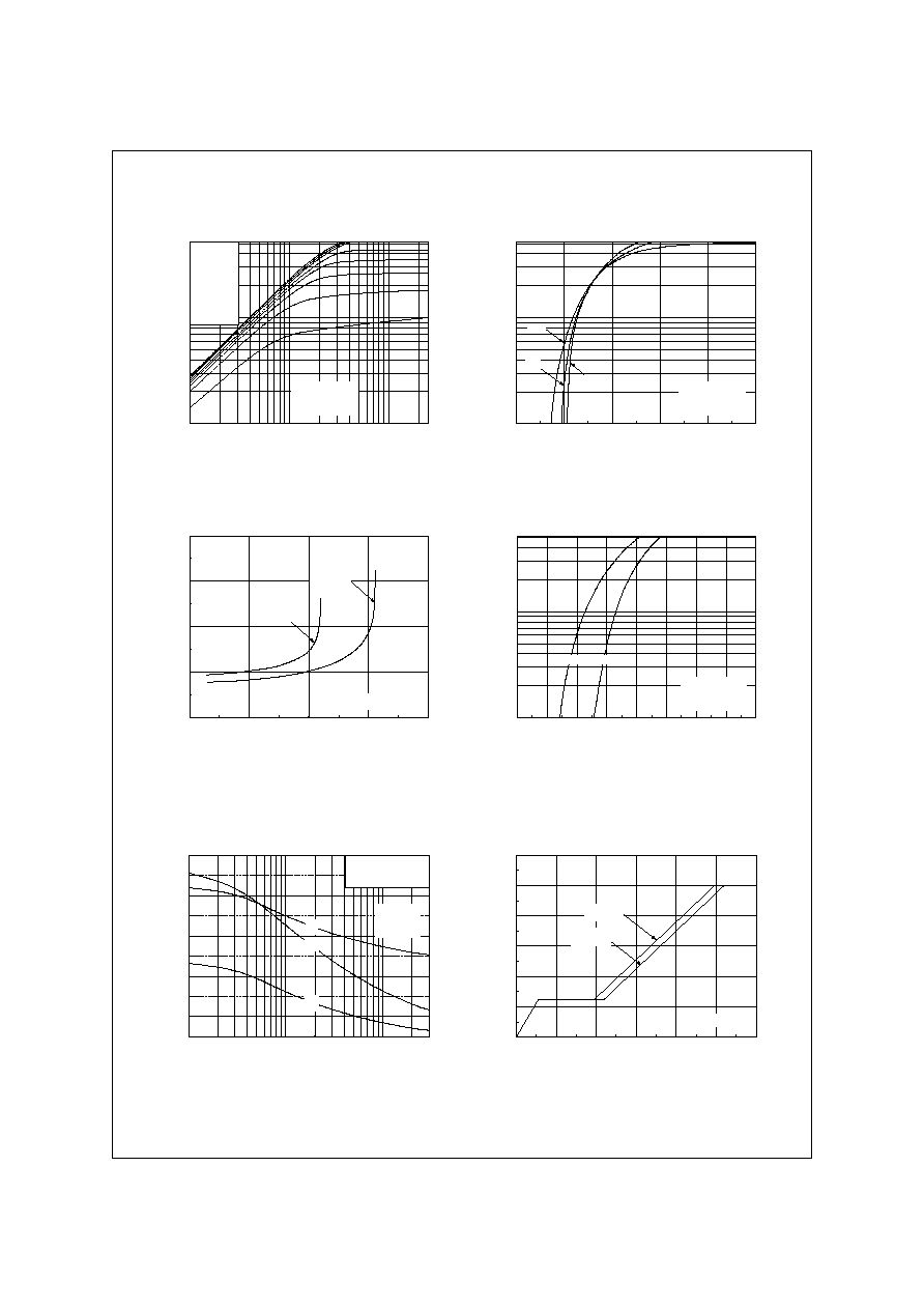
0.0
0.5
1.0
1.5
2.0
2.5
3.0
0
2
4
6
8
10
12
V
DS
= 48V
V
DS
= 30V
Note : I
D
= 1.3 A
V
GS
,
G
a
t
e
-
S
our
c
e
V
o
l
t
ag
e [
V
]
Q
G
, Total Gate Charge [nC]
10
-1
10
0
10
1
0
40
80
120
160
C
iss
= C
gs
+ C
gd
(C
ds
= shorted)
C
oss
= C
ds
+ C
gd
C
rss
= C
gd
Notes :
1. V
GS
= 0 V
2. f = 1 MHz
C
rss
C
oss
C
iss
C
a
pac
i
t
a
n
c
e
[
p
F]
V
DS
, Drain-Source Voltage [V]
0.2
0.4
0.6
0.8
1.0
1.2
1.4
1.6
1.8
10
-1
10
0
150
Notes :
1. V
GS
= 0V
2. 250
s Pulse Test
25
I
DR
,
R
e
v
e
r
s
e
Dr
a
i
n
Cu
r
r
e
n
t
[
A
]
V
SD
, Source-Drain voltage [V]
0
2
4
6
8
0.0
0.5
1.0
1.5
2.0
V
GS
= 5V
V
GS
= 10V
Note : T
J
= 25
R
DS
(
O
N)
[
],
D
r
ai
n-
S
o
ur
ce
O
n
-
R
e
s
i
s
t
a
nc
e
I
D
, Drain Current [A]
0
2
4
6
8
10
10
-1
10
0
150
25
-55
Notes :
1. V
DS
= 25V
2. 250
s Pulse Test
I
D
, D
r
a
i
n
C
u
r
r
e
n
t [A
]
V
GS
, Gate-Source Voltage [V]
10
-1
10
0
10
1
10
-1
10
0
V
GS
Top : 10.0 V
8.0 V
6.0 V
5.0 V
4.5 V
4.0 V
3.5 V
Bottom : 3.0 V
Notes :
1. 250
s Pulse Test
2. T
C
= 25
I
D
,
D
r
ai
n C
u
r
r
e
nt
[
A
]
V
DS
, Drain-Source Voltage [V]
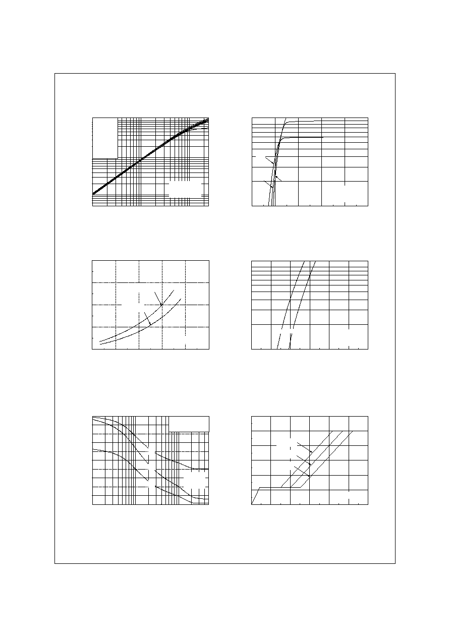
Typical Characteristics : N-Channel
Figure 5. Capacitance Characteristics
Figure 6. Gate Charge Characteristics
Figure 3. On-Resistance Variation vs.
Drain Current and Gate Voltage
Figure 4. Body Diode Forward Voltage
Variation vs. Source Current
and Temperature
Figure 2. Transfer Characteristics
Figure 1. On-Region Characteristics
©2000 Fairchild Semiconductor International
FQS
4900
Rev. A, August 2000
1 0
- 4
1 0
- 3
1 0
- 2
1 0
- 1
1 0
0
1 0
1
1 0
2
1 0
- 1
1 0
0
1 0
1
0 .0 1
N o te s :
1 . Z
J C
( t) = 6 2 . 5
/W M a x .
2 . D u ty F a c to r , D = t
1
/ t
2
3 . T
J M
- T
C
= P
D M
* Z
J C
( t)
s in g le p u ls e
D = 0 .5
0 .0 2
0 .2
0 .0 5
0 .1
Z
JC
(
t
)
,
T
her
m
a
l
R
e
s
pon
s
e
t
1
, S q u a re W a v e P u ls e D u ra tio n [s e c ]
25
50
75
100
125
150
0.0
0.3
0.6
0.9
1.2
1.5
I
D
,
Dr
a
i
n
Cu
r
r
e
n
t
[
A
]
T
C
, Case Temperature [
]
10
-1
10
0
10
1
10
2
10
-2
10
-1
10
0
10
1
1 ms
100 ms
1 s
DC
10 s
10 ms
Operation in This Area
is Limited by R
DS(on)
Notes :
1. T
C
= 25
o
C
2. T
J
= 150
o
C
3. Single Pulse
I
D
,
D
r
a
i
n
C
u
rre
n
t
[
A
]
V
DS
, Drain-Source Voltage [V]
-100
-50
0
50
100
150
200
0.0
0.5
1.0
1.5
2.0
2.5
Notes :
1. V
GS
= 10 V
2. I
D
= 0.65 A
R
DS
(
O
N)
,
(
N
or
m
a
l
i
z
e
d)
D
r
ai
n-
S
o
ur
c
e
O
n
-
R
es
i
s
t
a
nc
e
T
J
, Junction Temperature [
o
C]
-100
-50
0
50
100
150
200
0.8
0.9
1.0
1.1
1.2
Notes :
1. V
GS
= 0 V
2. I
D
= 250
A
BV
DSS
, (
N
o
r
m
a
liz
e
d
)
D
r
ai
n-
S
o
u
r
ce B
r
eak
d
o
w
n
V
o
l
t
age
T
J
, Junction Temperature [
o
C]
Typical Characteristics : N-Channel
(Continued)
Figure 9. Maximum Safe Operating Area
Figure 10. Maximum Drain Current
vs. Case Temperature
Figure 7. Breakdown Voltage Variation
vs. Temperature
Figure 8. On-Resistance Variation
vs. Temperature
Figure 11. Transient Thermal Response Curve
t
1
P
DM
t
2
©2000 Fairchild Semiconductor International
FQS490
0
Rev. A, August 2000
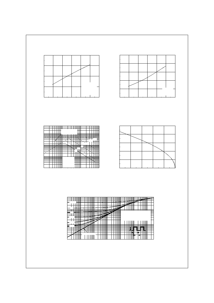
0
1
2
3
4
5
6
0
2
4
6
8
10
12
V
DS
= -150V
V
DS
= -60V
V
DS
= -240V
Note : I
D
= -0.3 A
-V
GS
,
G
a
te
-S
o
u
rc
e
V
o
l
t
a
g
e
[
V
]
Q
G
, Total Gate Charge [nC]
10
-1
10
0
10
1
0
50
100
150
200
250
C
iss
= C
gs
+ C
gd
(C
ds
= shorted)
C
oss
= C
ds
+ C
gd
C
rss
= C
gd
Notes :
1. V
GS
= 0 V
2. f = 1 MHz
C
rss
C
oss
C
iss
C
a
p
a
c
i
t
a
nc
e [
p
F
]
V
DS
, Drain-Source Voltage [V]
0.0
0.5
1.0
1.5
2.0
2.5
3.0
10
-1
10
0
150
Notes :
1. V
GS
= 0V
2. 250
s Pulse Test
25
-I
DR
,
Re
v
e
r
s
e
Dr
a
i
n
Cu
r
r
e
n
t
[
A
]
-V
SD
, Source-Drain Voltage [V]
0.0
0.3
0.6
0.9
1.2
1.5
10
15
20
25
30
Note : T
J
= 25
V
GS
= - 5V
V
GS
= - 10V
R
D
S
(
on)
[
],
D
r
a
i
n-
S
o
ur
c
e
O
n
-
R
es
i
s
t
a
nc
e
-I
D
, Drain Current [A]
0
2
4
6
8
10
10
-1
10
0
150
25
-55
Notes :
1. V
DS
= -25V
2. 250
s Pulse Test
-I
D
,
D
r
ai
n C
u
r
r
ent
[
A
]
-V
GS
, Gate-Source Voltage [V]
10
-1
10
0
10
1
10
-2
10
-1
10
0
V
GS
Top : -10.0 V
-8.0 V
-6.0 V
-5.0 V
-4.5 V
-4.0 V
-3.5 V
Bottom : -3.0 V
Notes :
1. 250
s Pulse Test
2. T
C
= 25
-I
D
,
D
r
ai
n C
u
r
r
ent
[
A
]
-V
DS
, Drain-Source Voltage [V]
Typical Characteristics : P-Channel
(Continued)
Figure 5. Capacitance Characteristics
Figure 6. Gate Charge Characteristics
Figure 3. On-Resistance Variation vs.
Drain Current and Gate Voltage
Figure 4. Body Diode Forward Voltage
Variation vs. Source Current
and Temperature
Figure 2. Transfer Characteristics
Figure 1. On-Region Characteristics