 | ÐлекÑÑоннÑй компоненÑ: FQU3N60 | СкаÑаÑÑ:  PDF PDF  ZIP ZIP |
Äîêóìåíòàöèÿ è îïèñàíèÿ www.docs.chipfind.ru
©2000 Fairchild Semiconductor International
April 2000
Rev. A, April 2000
FQ
D
3
N6
0
/
FQ
U3
N6
0
QFET
QFET
QFET
QFET
TM
FQD3N60 / FQU3N60
600V N-Channel MOSFET
General Description
These N-Channel enhancement mode power field effect
transistors are produced using Fairchild's proprietary,
planar stripe, DMOS technology.
This advanced technology has been especially tailored to
minimize on-state resistance, provide superior switching
performance, and withstand high energy pulse in the
avalanche and commutation mode. These devices are well
suited for high efficiency switch mode power supply.
Features
· 2.4A, 600V, R
DS(on)
= 3.6
@V
GS
= 10 V
· Low gate charge ( typical 10 nC)
· Low Crss ( typical 5.5 pF)
· Fast switching
· 100% avalanche tested
· Improved dv/dt capability
Absolute Maximum Ratings
T
C
= 25°C unless otherwise noted
Thermal Characteristics
Symbol
Parameter
FQD3N60 / FQU3N60
Units
V
DSS
Drain-Source Voltage
600
V
I
D
Drain Current
- Continuous (T
C
= 25°C)
2.4
A
- Continuous (T
C
= 100°C)
1.5
A
I
DM
Drain Current
- Pulsed
(Note 1)
9.6
A
V
GSS
Gate-Source Voltage
±
30
V
E
AS
Single Pulsed Avalanche Energy
(Note 2)
200
mJ
I
AR
Avalanche Current
(Note 1)
2.4
A
E
AR
Repetitive Avalanche Energy
(Note 1)
5.0
mJ
dv/dt
Peak Diode Recovery dv/dt
(Note 3)
4.5
V/ns
P
D
Power Dissipation (T
A
= 25°C) *
2.5
W
Power Dissipation (T
C
= 25°C)
50
W
- Derate above 25°C
0.4
W/°C
T
J
, T
STG
Operating and Storage Temperature Range
-55 to +150
°C
T
L
Maximum lead temperature for soldering purposes,
1/8
from case for 5 seconds
300
°C
Symbol
Parameter
Typ
Max
Units
R
JC
Thermal Resistance, Junction-to-Case
--
2.5
°C
W
R
JA
Thermal Resistance, Junction-to-Ambient *
--
50
°C
W
R
JA
Thermal Resistance, Junction-to-Ambient
--
110
°C
W
* When mounted on the minimum pad size recommended (PCB Mount)
! "
!
!
!
"
"
"
! "
!
!
!
"
"
"
S
D
G
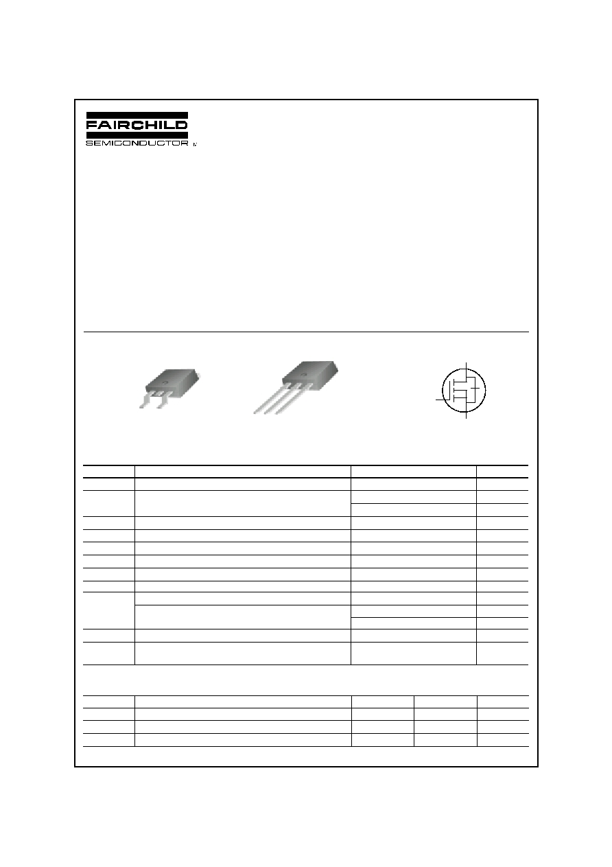
I-PAK
FQU Series
D-PAK
FQD Series
G
S
D
G
S
D
©2000 Fairchild Semiconductor International
FQD3N60 /
FQU3N60
(Note 4)
(Note 4, 5)
(Note 4, 5)
(Note 4)
Rev. A, April 2000
Electrical Characteristics
T
C
= 25°C unless otherwise noted
Notes:
1. Repetitive Rating : Pulse width limited by maximum junction temperature
2. L = 64mH, I
AS
= 2.4A, V
DD
= 50V, R
G
= 25
,
Starting T
J
= 25°C
3. I
SD
3.0A, di/dt
200A/
µ
s, V
DD
BV
DSS,
Starting T
J
= 25°C
4. Pulse Test : Pulse width
300
µ
s, Duty cycle
2%
5. Essentially independent of operating temperature
Symbol
Parameter
Test Conditions
Min
Typ
Max
Units
Off Characteristics
BV
DSS
Drain-Source Breakdown Voltage
V
GS
= 0 V, I
D
= 250
µ
A
600
--
--
V
BV
DSS
/
T
J
Breakdown Voltage Temperature
Coefficient
I
D
= 250
µ
A, Referenced to 25°C
--
0.6
--
V/°C
I
DSS
Zero Gate Voltage Drain Current
V
DS
= 600 V, V
GS
= 0 V
--
--
10
µ
A
V
DS
= 480 V, T
C
= 125°C
--
--
100
µ
A
I
GSSF
Gate-Body Leakage Current, Forward
V
GS
= 30 V, V
DS
= 0 V
--
--
100
nA
I
GSSR
Gate-Body Leakage Current, Reverse
V
GS
= -30 V, V
DS
= 0 V
--
--
-100
nA
On Characteristics
V
GS(th)
Gate Threshold Voltage
V
DS
= V
GS
, I
D
= 250
µ
A
3.0
--
5.0
V
R
DS(on)
Static Drain-Source
On-Resistance
V
GS
= 10 V, I
D
= 1.2 A
--
2.8
3.6
g
FS
Forward Transconductance
V
DS
= 50 V, I
D
= 1.2 A
--
2.4
--
S
Dynamic Characteristics
C
iss
Input Capacitance
V
DS
= 25 V, V
GS
= 0 V,
f = 1.0 MHz
--
350
450
pF
C
oss
Output Capacitance
--
50
65
pF
C
rss
Reverse Transfer Capacitance
--
5.5
7.5
pF
Switching Characteristics
t
d(on)
Turn-On Delay Time
V
DD
= 300 V, I
D
= 3.0 A,
R
G
= 25
--
10
30
ns
t
r
Turn-On Rise Time
--
30
70
ns
t
d(off)
Turn-Off Delay Time
--
20
50
ns
t
f
Turn-Off Fall Time
--
30
70
ns
Q
g
Total Gate Charge
V
DS
= 480 V, I
D
= 3.0 A,
V
GS
= 10 V
--
10
13
nC
Q
gs
Gate-Source Charge
--
2.7
--
nC
Q
gd
Gate-Drain Charge
--
4.9
--
nC
Drain-Source Diode Characteristics and Maximum Ratings
I
S
Maximum Continuous Drain-Source Diode Forward Current
--
--
2.4
A
I
SM
Maximum Pulsed Drain-Source Diode Forward Current
--
--
9.6
A
V
SD
Drain-Source Diode Forward Voltage
V
GS
= 0 V, I
S
= 2.4 A
--
--
1.4
V
t
rr
Reverse Recovery Time
V
GS
= 0 V, I
S
= 3.0 A,
dI
F
/ dt = 100 A/
µ
s
--
210
--
ns
Q
rr
Reverse Recovery Charge
--
1.2
--
µ
C
©2000 Fairchild Semiconductor International
FQ
D
3
N6
0
/
FQ
U3
N6
0
Rev. A, April 2000
0.2
0.4
0.6
0.8
1.0
1.2
1.4
1.6
10
-1
10
0
25
150
Notes :
1. V
GS
= 0V
2. 250
s Pulse Test
I
DR
,
R
e
v
e
r
s
e D
r
ai
n C
u
r
r
e
n
t
[
A
]
V
SD
, Source-Drain Voltage [V]
2
4
6
8
10
10
-1
10
0
Notes :
1. V
DS
= 50V
2. 250
s Pulse Test
-55
150
25
I
D
, D
r
a
i
n
C
u
rre
n
t
[A
]
V
GS
, Gate-Source Voltage [V]
10
-1
10
0
10
1
10
-2
10
-1
10
0
V
GS
Top : 15.0 V
10.0 V
8.0 V
7.0 V
6.5 V
6.0 V
Bottom : 5.5 V
Notes :
1. 250
s Pulse Test
2. T
C
= 25
I
D
, D
r
a
i
n
C
u
rre
n
t
[A
]
V
DS
, Drain-Source Voltage [V]
0
2
4
6
8
10
0
2
4
6
8
10
12
V
DS
= 300V
V
DS
= 120V
V
DS
= 480V
Note : I
D
= 3.0 A
V
GS
,
G
a
t
e
-
S
our
ce
Vol
t
ag
e
[
V
]
Q
G
, Total Gate Charge [nC]
10
-1
10
0
10
1
0
100
200
300
400
500
600
C
iss
= C
gs
+ C
gd
(C
ds
= shorted)
C
oss
= C
ds
+ C
gd
C
rss
= C
gd
Notes :
1. V
GS
= 0 V
2. f = 1 MHz
C
rss
C
oss
C
iss
C
a
paci
t
an
ce [
p
F
]
V
DS
, Drain-Source Voltage [V]
0
1
2
3
4
5
6
7
0
2
4
6
8
10
12
V
GS
= 20V
V
GS
= 10V
Note : T
J
= 25
R
DS
(
O
N
)
[
],
D
r
ai
n-
Sour
c
e
O
n
-
R
e
s
i
s
t
a
nc
e
I
D
, Drain Current [A]
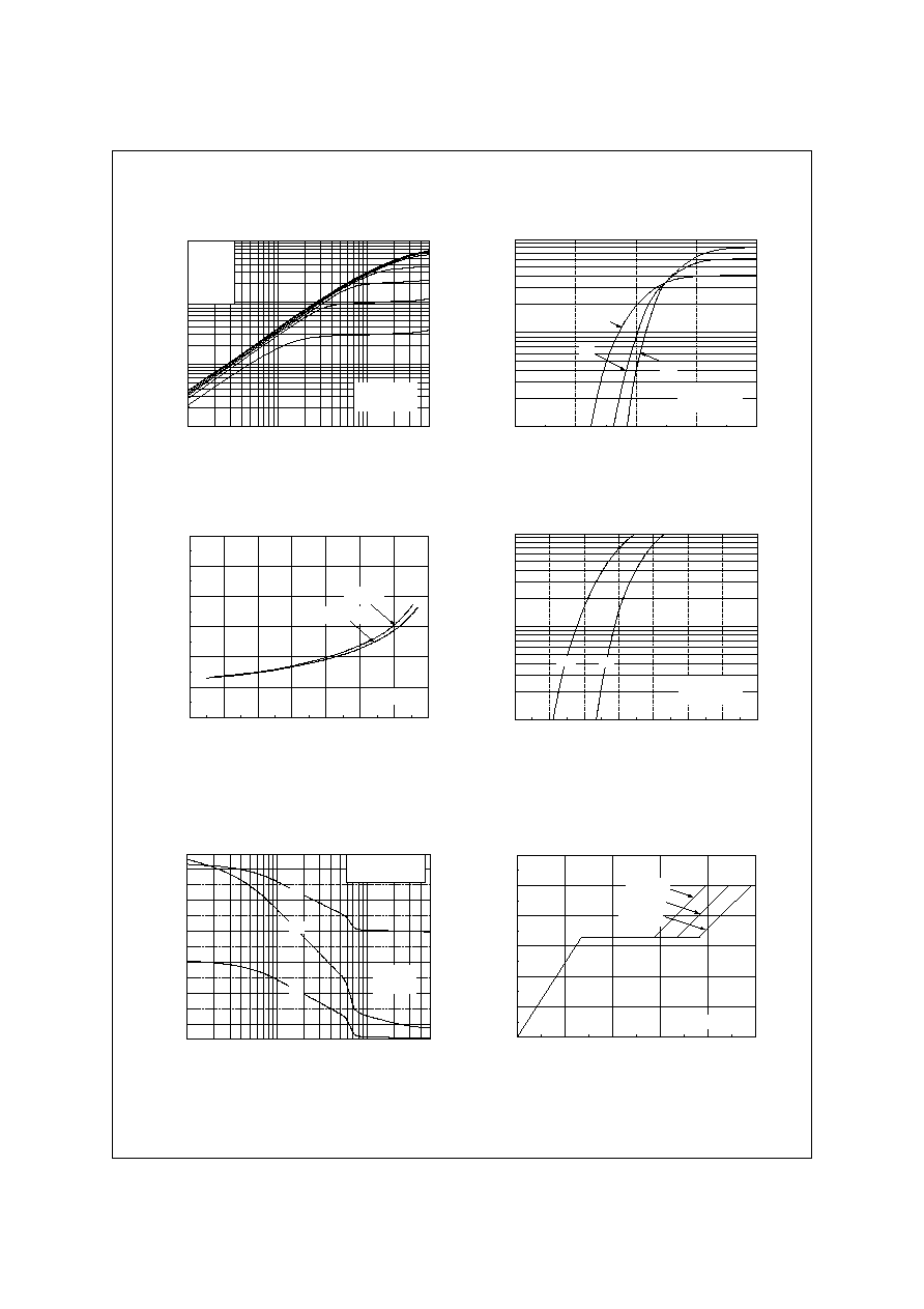
Typical Characteristics
Figure 5. Capacitance Characteristics
Figure 6. Gate Charge Characteristics
Figure 3. On-Resistance Variation vs.
Drain Current and Gate Voltage
Figure 4. Body Diode Forward Voltage
Variation vs. Source Current
and Temperature
Figure 2. Transfer Characteristics
Figure 1. On-Region Characteristics
©2000 Fairchild Semiconductor International
FQD3N60 /
FQU3N60
Rev. A, April 2000
1 0
-5
1 0
-4
1 0
-3
1 0
-2
1 0
-1
1 0
0
1 0
1
1 0
-2
1 0
-1
1 0
0
N o te s :
1 . Z
J C
( t ) = 2 . 5
/W M a x .
2 . D u ty F a c t o r , D = t
1
/t
2
3 . T
J M
- T
C
= P
D M
* Z
J C
( t )
s in g le p u ls e
D = 0 . 5
0 .0 2
0 .2
0 .0 5
0 .1
0 .0 1
Z
JC
(
t
)
,
T
h
er
m
a
l
R
e
s
pon
s
e
t
1
, S q u a r e W a v e P u ls e D u r a t io n [ s e c ]
25
50
75
100
125
150
0.0
0.5
1.0
1.5
2.0
2.5
I
D
,
D
r
ai
n C
u
r
r
e
n
t
[
A
]
T
C
, Case Temperature [
]
10
0
10
-2
10
-1
10
0
10
1
10
µ
s
DC
10 ms
1 ms
100
µ
s
Operation in This Area
is Limited by R
DS(on)
Notes :
1. T
C
= 25
o
C
2. T
J
= 150
o
C
3. Single Pulse
I
D
, D
r
a
i
n
C
u
r
r
e
n
t [A
]
V
DS
, Drain-Source Voltage [V]
-100
-50
0
50
100
150
200
0.0
0.5
1.0
1.5
2.0
2.5
3.0
Notes :
1. V
GS
= 10 V
2. I
D
= 1.5 A
R
DS
(
O
N
)
,
(
N
or
m
a
l
i
z
ed)
D
r
ai
n-
S
our
ce O
n
-
R
esi
s
t
a
nce
T
J
, Junction Temperature [
o
C]
-100
-50
0
50
100
150
200
0.8
0.9
1.0
1.1
1.2
Notes :
1. V
GS
= 0 V
2. I
D
= 250
A
BV
DS
S
,
(
N
o
r
m
a
liz
e
d
)
D
r
a
i
n-
S
o
ur
c
e
B
r
ea
k
d
o
w
n V
o
l
t
ag
e
T
J
, Junction Temperature [
o
C]
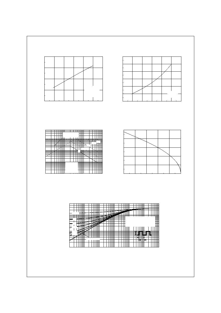
Typical Characteristics
(Continued)
Figure 9. Maximum Safe Operating Area
Figure 10. Maximum Drain Current
vs. Case Temperature
Figure 7. Breakdown Voltage Variation
vs. Temperature
Figure 8. On-Resistance Variation
vs. Temperature
Figure 11. Transient Thermal Response Curve
t
1
P
DM
t
2
©2000 Fairchild Semiconductor International
FQ
D
3
N6
0
/
FQ
U3
N6
0
Rev. A, April 2000
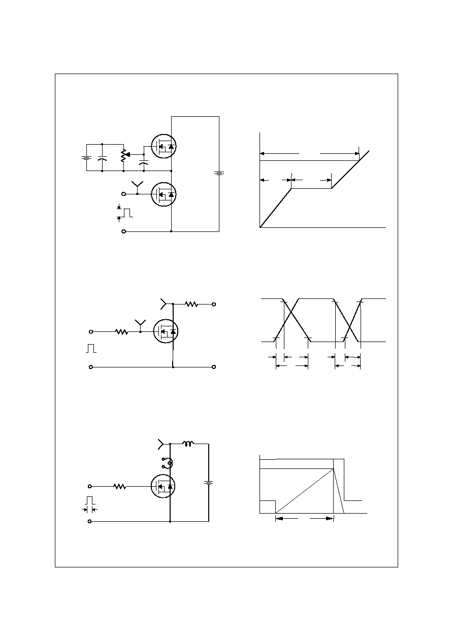
Gate Charge Test Circuit & Waveform
Resistive Switching Test Circuit & Waveforms
Unclamped Inductive Switching Test Circuit & Waveforms
Charge
V
GS
10V
Q
g
Q
gs
Q
gd
3mA
V
GS
DUT
V
DS
300nF
50K
200nF
12V
Same Type
as DUT
Charge
V
GS
10V
Q
g
Q
gs
Q
gd
3mA
V
GS
DUT
V
DS
300nF
50K
200nF
12V
Same Type
as DUT
V
GS
V
DS
10%
90%
t
d(on)
t
r
t
on
t
off
t
d(off)
t
f
V
DD
10V
V
DS
R
L
DUT
R
G
V
GS
V
GS
V
DS
10%
90%
t
d(on)
t
r
t
on
t
off
t
d(off)
t
f
V
DD
10V
V
DS
R
L
DUT
R
G
V
GS
E
AS
=
L I
AS
2
----
2
1
--------------------
BV
DSS
- V
DD
BV
DSS
V
DD
V
DS
BV
DSS
t
p
V
DD
I
AS
V
DS
(t)
I
D
(t)
Time
10V
DUT
R
G
L
I
D
t
p
E
AS
=
L I
AS
2
----
2
1
E
AS
=
L I
AS
2
----
2
1
----
2
1
--------------------
BV
DSS
- V
DD
BV
DSS
V
DD
V
DS
BV
DSS
t
p
V
DD
I
AS
V
DS
(t)
I
D
(t)
Time
10V
DUT
R
G
L
L
I
D
I
D
t
p
©2000 Fairchild Semiconductor International
FQD3N60 /
FQU3N60
Rev. A, April 2000
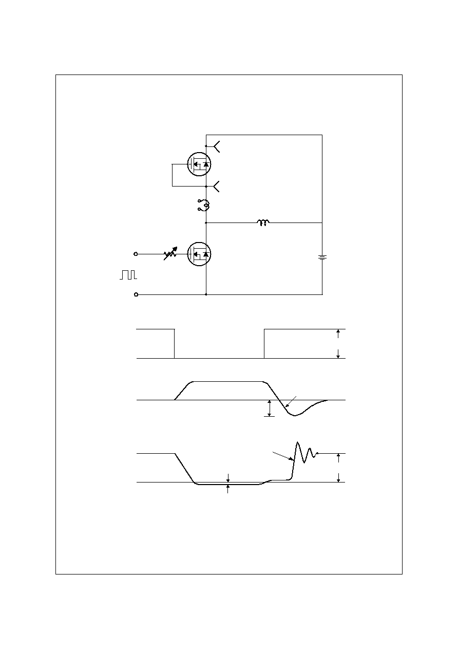
Peak Diode Recovery dv/dt Test Circuit & Waveforms
DUT
V
DS
+
_
Driver
R
G
Same Type
as DUT
V
GS
· dv/dt controlled by R
G
· I
SD
controlled by pulse period
V
DD
L
I
SD
10V
V
GS
( Driver )
I
SD
( DUT )
V
DS
( DUT )
V
DD
Body Diode
Forward Voltage Drop
V
SD
I
FM
, Body Diode Forward Current
Body Diode Reverse Current
I
RM
Body Diode Recovery dv/dt
di/dt
D =
Gate Pulse Width
Gate Pulse Period
--------------------------
DUT
V
DS
+
_
Driver
R
G
Same Type
as DUT
V
GS
· dv/dt controlled by R
G
· I
SD
controlled by pulse period
V
DD
L
L
I
SD
10V
V
GS
( Driver )
I
SD
( DUT )
V
DS
( DUT )
V
DD
Body Diode
Forward Voltage Drop
V
SD
I
FM
, Body Diode Forward Current
Body Diode Reverse Current
I
RM
Body Diode Recovery dv/dt
di/dt
D =
Gate Pulse Width
Gate Pulse Period
--------------------------
D =
Gate Pulse Width
Gate Pulse Period
--------------------------
©2000 Fairchild Semiconductor International
FQ
D
3
N6
0
/
FQ
U3
N6
0
Rev. A, April 2000
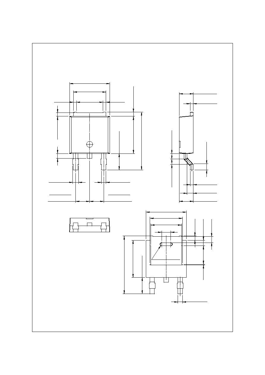
Package Dimensions
6.60
±
0.20
2.30
±
0.10
0.50
±
0.10
5.34
±
0.30
0.70
±
0.20
0.60
±
0.20
0.80
±
0.20
9.50
±
0.30
6.10
±
0.20
2.70
±
0.20
9.50
±
0.30
6.10
±
0.20
2.70
±
0.20
MIN0.55
0.76
±
0.10
0.50
±
0.10
1.02
±
0.20
2.30
±
0.20
6.60
±
0.20
0.76
±
0.10
(5.34)
(1.50)
(2XR0.25)
(5.04)
0.89
±
0.10
(0.10)
(3.05)
(1.00)
(0.90)
(0.70)
0.91
±
0.10
2.30TYP
[2.30
±
0.20]
2.30TYP
[2.30
±
0.20]
MAX0.96
(4.34)
(0.50)
(0.50)
DPAK
©2000 Fairchild Semiconductor International
FQD3N60 /
FQU3N60
Rev. A, April 2000
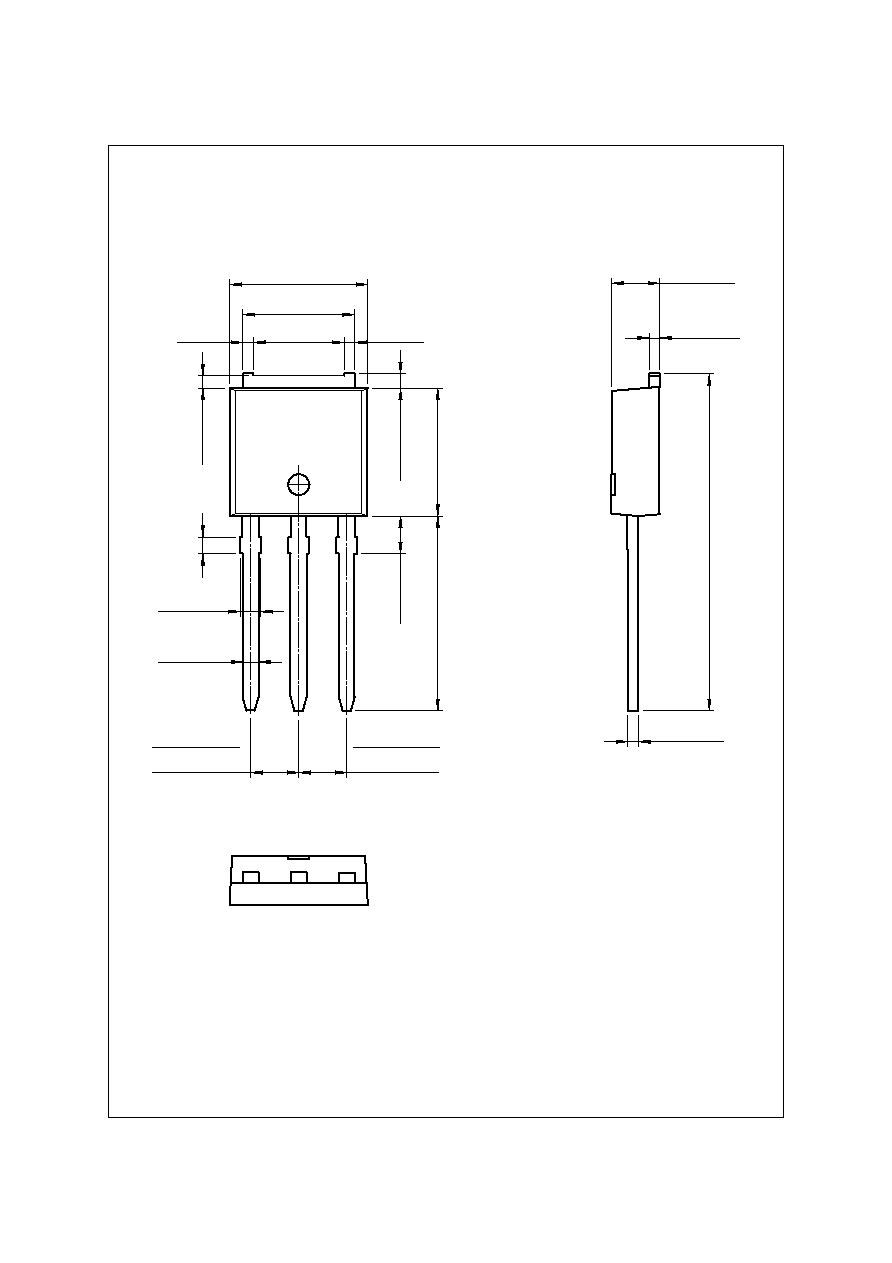
Package Dimensions
(Continued)
6.60
±
0.20
0.76
±
0.10
MAX0.96
2.30TYP
[2.30
±
0.20]
2.30TYP
[2.30
±
0.20]
0.60
±
0.20
0.80
±
0.10
1.80
±
0.20
9.30
±
0.30
16.10
±
0.30
6.10
±
0.20
0.70
±
0.20
5.34
±
0.20
0.50
±
0.10
0.50
±
0.10
2.30
±
0.20
(0.50)
(0.50)
(4.34)
IPAK
©2000 Fairchild Semiconductor International
Rev. A, January 2000
TRADEMARKS
The following are registered and unregistered trademarks Fairchild Semiconductor owns or is authorized to use and is
not intended to be an exhaustive list of all such trademarks.
ACExTM
BottomlessTM
CoolFETTM
CROSSVOLTTM
E
2
CMOSTM
FACTTM
FACT Quiet SeriesTM
FAST
®
FASTrTM
GTOTM
HiSeCTM
ISOPLANARTM
MICROWIRETM
POPTM
PowerTrench
®
QFETTM
QSTM
Quiet SeriesTM
SuperSOTTM-3
SuperSOTTM-6
SuperSOTTM-8
SyncFETTM
TinyLogicTM
UHCTM
VCXTM
DISCLAIMER
FAIRCHILD SEMICONDUCTOR RESERVES THE RIGHT TO MAKE CHANGES WITHOUT FURTHER NOTICE TO ANY
PRODUCTS HEREIN TO IMPROVE RELIABILITY, FUNCTION OR DESIGN. FAIRCHILD DOES NOT ASSUME ANY
LIABILITY ARISING OUT OF THE APPLICATION OR USE OF ANY PRODUCT OR CIRCUIT DESCRIBED HEREIN;
NEITHER DOES IT CONVEY ANY LICENSE UNDER ITS PATENT RIGHTS, NOR THE RIGHTS OF OTHERS.
LIFE SUPPORT POLICY
FAIRCHILD'S PRODUCTS ARE NOT AUTHORIZED FOR USE AS CRITICAL COMPONENTS IN LIFE SUPPORT
DEVICES OR SYSTEMS WITHOUT THE EXPRESS WRITTEN APPROVAL OF FAIRCHILD SEMICONDUCTOR
INTERNATIONAL.
As used herein:
1. Life support devices or systems are devices or systems
which, (a) are intended for surgical implant into the body,
or (b) support or sustain life, or (c) whose failure to perform
when properly used in accordance with instructions for use
provided in the labeling, can be reasonably expected to
result in significant injury to the user.
2. A critical component is any component of a life support
device or system whose failure to perform can be
reasonably expected to cause the failure of the life support
device or system, or to affect its safety or effectiveness.
PRODUCT STATUS DEFINITIONS
Definition of Terms
Datasheet Identification
Product Status
Definition
Advance Information
Formative or In
Design
This datasheet contains the design specifications for
product development. Specifications may change in
any manner without notice.
Preliminary
First Production
This datasheet contains preliminary data, and
supplementary data will be published at a later date.
Fairchild Semiconductor reserves the right to make
changes at any time without notice in order to improve
design.
No Identification Needed
Full Production
This datasheet contains final specifications. Fairchild
Semiconductor reserves the right to make changes at
any time without notice in order to improve design.
Obsolete
Not In Production
This datasheet contains specifications on a product
that has been discontinued by Fairchild semiconductor.
The datasheet is printed for reference information only.