Äîêóìåíòàöèÿ è îïèñàíèÿ www.docs.chipfind.ru
©2003 Fairchild Semiconductor Corporation
www.fairchildsemi.com
Rev.1.0.1
Features
· Wide Operating Frequency Range up to 150kHz
· Lowest Cost SMPS Solution
· Lowest External Components
· Low Start up Current (Max:170uA)
· Low Operating Current (Max:15mA)
· Internal High Voltage SenseFET
· Built-in Auto Restart Circuit
· Over Voltage Protection (Auto Restart Mode)
· Over Load Protection (Auto Restart Mode)
· Over Current Protection (Auto Restart Mode)
· Internal Thermal Protection(Auto Restart Mode)
· Pulse By Pulse Over Current Limiting
· Internal Burst Mode Controller for Stand-by Mode
· Under Voltage Lockout With Hysteresis
· External Sync. Terminal
Application
· Monitor SMPS
Description
The Fairchild Power Switch(FPS) product family are
specially designed for an off line SMPS with minimal
external components. The Fairchild Power Switch(FPS)
consists of a high voltage power SenseFET and a current
mode PWM IC. Included PWM controller features the
integrated fixed oscillator, the under voltage lockout, the
optimized gate turn on/turn off driver, the thermal shut
down protection, the over voltage protection, and the
temperature compensated precision current sources for the
loop compensation and the fault protection circuitry.
Compared to a discrete MOSFET and a controller or a RCC
switching converter solution, a Fairchild Power Switch(FPS)
can reduce the total component count, design size, and
weight and at the same time increase efficiency,
productivity, and system reliability. It has a basic platform
well suited for the cost effective monitor power supply.
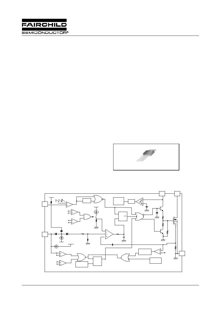
TO-220-5L
1
1. Drain 2. Gnd 3. V
CC
4. Feedback 5. Sync
Internal Block Diagram
S
R
Q
S
R
Q
TSD
(Tj=160 )
Ifb
1
1
1
1
3
3
3
3
5
5
5
5
4
4
4
4
2
2
2
2
Vref
Rsenese
2.5R
R
Vref
Internal
Bias
Vref
UVLO
Ron
Roff
PWM
OCL
Burst mode
controller
Filter
(130nsec)
UVLO Reset
(Vcc=9V)
OLP
OVP
Vth=7.5V
Vcc
Vth=30V
Vth=1V
Vfb Offset
Idelay
Vcc
Vfb
Vth=1V
Vcc
Vth=11V/12V
OSC
Vref
Vpp=5.8/7.2V
Drain
Drain
Drain
Drain
Vcc
Vcc
Vcc
Vcc
SoftStart
SoftStart
SoftStart
SoftStart
& Sync
& Sync
& Sync
& Sync
Feedback
Feedback
Feedback
Feedback
GND
GND
GND
GND
FS6S0965RCB
Fairchild Power Switch(FPS)
FS6S0965RCB
2
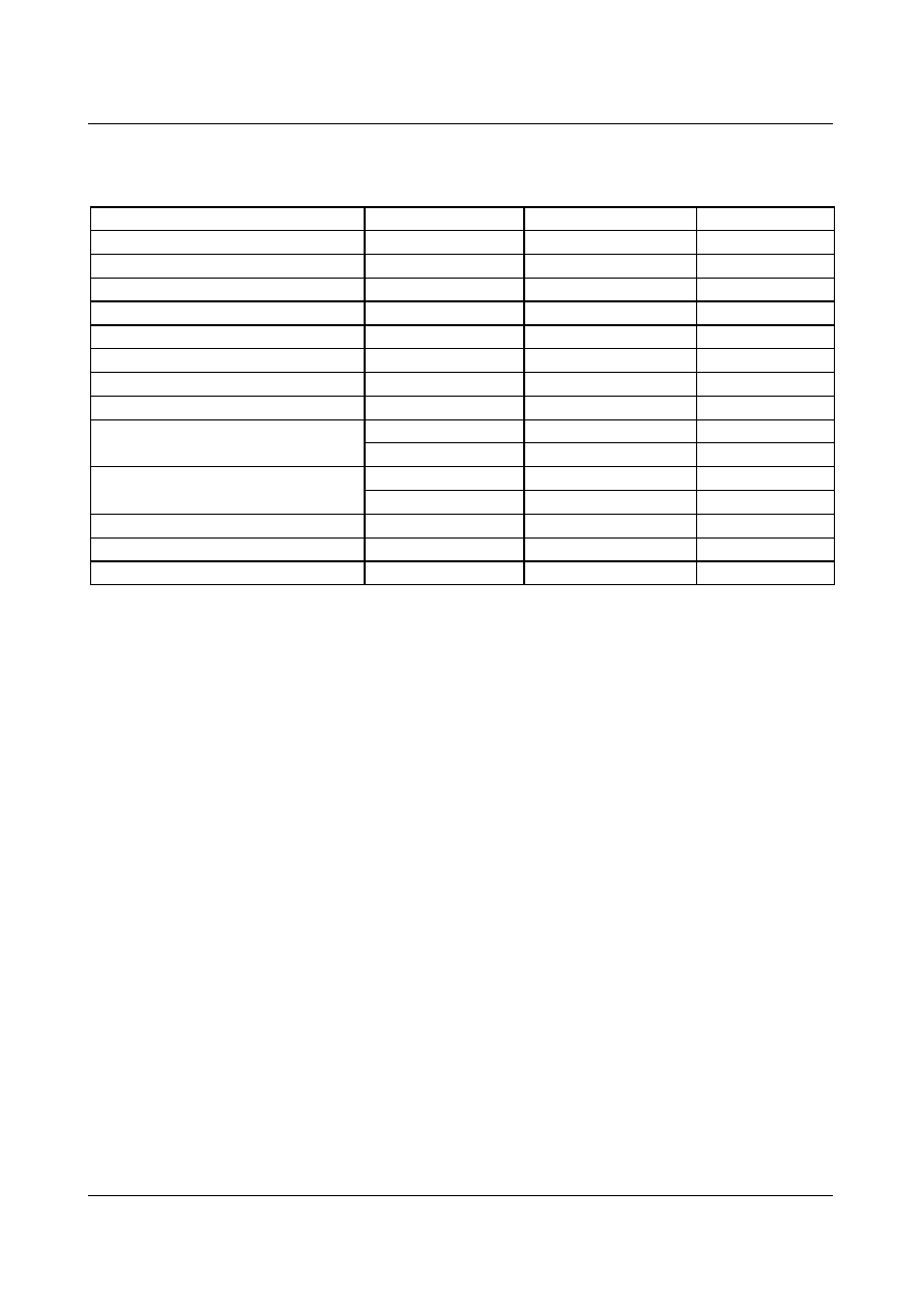
Absolute Maximum Ratings
(Ta=25
°
C, unless otherwise specified)
Notes:
1. Tj=25
°
C to 150
°
C
2. Repetitive rating: Pulse width limited by maximum junction temperature
3. L=14.5mH, starting Tj=25
°
C
4. L=13uH, starting Tj=25
°
C
Parameter
Symbol
Value
Unit
Drain-Gate Voltage (R
GS
=1M
)
V
DGR
650
V
Gate-Source (GND) Voltage
V
GS
±
30
V
Drain Current Pulsed
(2)
I
DM
32.4
A
DC
Single Pulsed Avalanche Energy
(3)
E
AS
515
mJ
Single Pulsed Avalanche Current
(4)
I
AS
25
A
Continuous Drain Current (Tc = 25
°
C)
I
D
8.1
A
DC
Continuous Drain Current (T
C
=100
°
C)
I
D
5.1
A
DC
Supply Voltage
V
CC
35
V
Input Voltage Range
V
FB
-0.3 to V
CC
V
V
S_S
-0.3 to 10
V
Total Power Dissipation
P
D
(Watt H/S)
155
W
Derating
1.243
W/
°
C
Operating Junction Temperature
T
j
+150
°
C
Operating Ambient Temperature
T
A
-25 to +85
°
C
Storage Temperature Range
T
STG
-55 to +150
°
C
FS6S0965RCB
3
Electrical Characteristics (SenseFET part)
(Ta=25
°
C unless otherwise specified)
Notes:
1.Pulse test : Pulse width
300
µ
S, duty 2%
2.
Parameter
Symbol
Condition
Min.
Typ.
Max.
Unit
Drain-Source Breakdown Voltage
BV
DSS
V
GS
=0V, I
D
=250
µ
A
650
-
-
V
Zero Gate Voltage Drain Current
I
DSS
V
DS
=650V, V
GS
=0V
-
-
200
µ
A
V
DS
=520V
V
GS
=0V, T
C
=125
°
C
-
-
300
µ
A
Static Drain-Source On Resistance
(1)
R
DS(ON)
V
GS
=10V, I
D
=1.8A
-
1.0
1.2
Forward Transconductance
(2)
gfs
V
DS
=50V, I
D
=1.8A
-
-
-
S
Input Capacitance
Ciss
V
GS
=0V, V
DS
=25V,
f = 1MHz
-
1300
-
pF
Output Capacitance
Coss
-
135
-
Reverse Transfer Capacitance
Crss
-
25
-
Turn On Delay Time
td(on)
V
DD
=325V, I
D
=6.5A
(MOSFET switching
time is essentially
independent of
operating temperature)
-
25
-
nS
Rise Time
tr
-
75
-
Turn Off Delay Time
td(off)
-
130
-
Fall Time
tf
-
70
-
Total Gate Charge
(Gate-Source+Gate-Drain)
Qg
V
GS
=10V, I
D
=6.5A,
V
DS
=520V (MOSFET
switching time is essentially
independent of
operating temperature)
-
45
60
nC
Gate-Source Charge
Qgs
-
8
-
Gate-Drain (Miller) Charge
Qgd
-
21
-
S
1
R
----
=
FS6S0965RCB
4
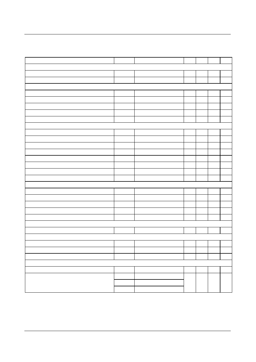
Electrical Characteristics
(Continued)
(Ta=25
°
C unless otherwise specified)
Note:
1. These parameters are the current flowing in the control IC.
2. These parameters, although guaranteed, are tested in the EDS(wafer test) process.
3. These parameters indicate the inductor current.
4. These parameters, although guranteed at the design, are not tested in the mass production
Parameter
Symbol
Condition
Min. Typ. Max. Unit
UVLO SECTION
Start Threshold Voltage
V
START
V
FB
=GND
14
15
16
V
Stop Threshold Voltage
V
STOP
V
FB
=GND
8
9
10
V
OSCILLATOR SECTION
Initial Frequency
F
OSC
-
22
25
28
kHz
Voltage Stability
F
STABLE
12V
Vcc
23V
0
1
3
%
Temperature Stability (4)
F
OSC
-25
°
C
Ta
85
°
C
0
±
5
±10
%
Maximum Duty Cycle
D
MAX
-
92
95
98
%
Minimum Duty Cycle
D
MIN
-
-
-
0
%
FEEDBACK SECTION
Feedback Source Current
I
FB
V
FB
=GND
0.7
0.9
1.1
mA
Shutdown Feedback Voltage
V
SD
Vfb
6.9V
6.9
7.5
8.1
V
Shutdown Delay Current
Idelay
V
FB
=5V
1.6
2.0
2.4
µ
A
SYNC & SOFTSTART SECTION
Softstart Vortage
V
SS
Vfb=2
4.7
5.0
5.3
V
Softstart Current
I
SS
Vss=V
0.8
1.0
1.2
mA
Sync High Threshold Voltage
V
SYNCH
Vcc=16V,Vfb=5V
-
7.2
-
V
Sync Low Threshold Voltage
V
SYNCL
Vcc=16V,Vfb=5V
-
5.8
-
V
BURST MODE SECTION
Burst Mode Low Threshold Voltage
V
BURL
Vfb=0V
10.4 11.0 11.6
V
Burst Mode High Threshold Voltage
V
BURH
Vfb=0V
11.4 12.0 12.6
V
Burst Mode Enable Feedback Voltage(4)
V
BEN
Vcc=10.5V
0.7
1.0
1.3
V
Burst Mode Peak Current Limit(3)
I
BU_PK
Vcc=10.5V
0.45
0.6
0.75
V
Burst Mode Frequency
F
BUR
Vcc=10.5V, Vfb=0V
40
50
60
kHz
CURRENT LIMIT(SELF-PROTECTION)SECTION
Peak Current Limit(3)
I
OVER
-
5.28
6.0
6.72
A
PROTECTION SECTION
Over Voltage Protection
V
OVP
Vcc
27V
27
30
33
V
Over Current Latch Voltage (2)
V
OCL
-
0.9
1.0
1.1
V
Thermal Shutdown Temperature(4)
T
SD
-
140
160
-
°
C
TOTAL DEVICE SECTION
Start Up Current
I
START
Vfb=GND, V
CC
=14V
-
0.1
0.17
mA
Operating Supply Current (1)
I
OP
Vfb=GND, V
CC
=16V
-
10
15
mA
I
OP(MIN)
Vfb=GND, V
CC
=10V
I
OP(MAX)
Vfb=GND, V
CC
=28V
FS6S0965RCB
5
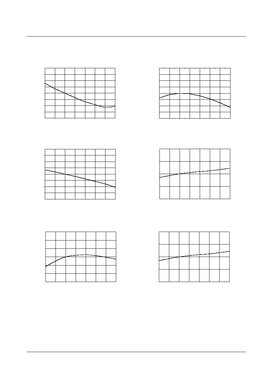
Typical Performance Characteristics
Figure 1. Start Up Current vs. Temp.
Figure 2. Operating Current vs. Temp.
Figure 3. Start Threshold Voltage
vs. Temp.
Figure 4. Stop Threshold Voltage vs. Temp.
Figure 5. Initial Frequency
vs. Temp.
Figure 6. Maximum Duty
vs. Temp.
-25
0
25
50
75
100
125
150
0.050
0.075
0.100
0.125
0.150 [mA]
Start Up Current vs. Temp
Temp
-25
0
25
50
75
100
125
150
9.0
9.5
10.0
10.5
11.0
[mA]
Operating Current vs. Temp
Temp
-25
0
25
50
75
100
125
150
14.0
14.5
15.0
15.5
16.0 [V]
Start Threshold Voltage vs. Temp
Temp
-25
0
25
50
75
100
125
150
94.0
94.5
95.0
95.5
96.0
[%]
Maximum Duty vs. Temp
Temp
-25
0
25
50
75
100
125
150
22
23
24
25
26
27
28
[KHz]
Initial Freqency vs. Temp
Temp
-25
0
25
50
75
100
125
150
94.0
94.5
95.0
95.5
96.0
[%]
Maximum Duty vs. Temp
Temp