 | –≠–ª–µ–∫—Ç—Ä–æ–Ω–Ω—ã–π –∫–æ–º–ø–æ–Ω–µ–Ω—Ç: FS6X0420R | –°–∫–∞—á–∞—Ç—å:  PDF PDF  ZIP ZIP |

©2006 Fairchild Semiconductor Corporation
1
www.fairchildsemi.com
March 2006
FS6X0420RJ/ FS6X0720RJ/ FS6X1220RJ Rev. 1.0.1
FS6
X
04
20
RJ
/ FS
6X0
7
2
0
RJ/
FS6X
12
20RJ
Fa
irchi
l
d Pow
e
r S
witch
(FP
S
TM)
FPS
TM
is a trademark of Fairchild Semiconductor Corporation
FS6X0420RJ/ FS6X0720RJ/ FS6X1220RJ
Fairchild Power Switch (FPSTM)
Features
Current Mode PWM Control with a Fixed Operating Fre-
quency (300kHz)
Pulse by Pulse Current Limit
Over Load Protection
Over Voltage Protection
Thermal Shutdown
Line Under Voltage Detection and Sleep on/off Function
Internal High Voltage SenseFET (200V)
Supports Forward or Flyback Topology
Applications
DC-DC Converter
PoE Device
Related Application Notes
AN4137 - Design Guidelines for Off-line Flyback Converters
Using Fairchild Power Switch (FPS)
AN4140 - Transformer Design Consideration for Off-line Fly-
back Converters using Fairchild Power Switch
AN4141 - Troubleshooting and Design Tips for Fairchild
Power Switch Flyback Applications
AN4148 - Audible Noise Reduction Techniques for FPS
Applications
Description
The FS6X-Series is specially designed for off-line DC-DC con-
verters with minimal external components. This device com-
bines a current mode PWM controller with a high voltage power
SenseFET in a single package. The PWM controller includes
integrated fixed frequency oscillator, line under voltage lockout,
sleep on/off function, thermal shutdown protection, over voltage
protection, pulse-by-pulse current limit, and temperature com-
pensated precise current sources for a loop compensation.
Compared with the discrete MOSFET and PWM controller solu-
tion, the FS6X-Series can reduce total cost, component count,
size, and weight, while simultaneously increasing efficiency,
productivity, and system reliability.
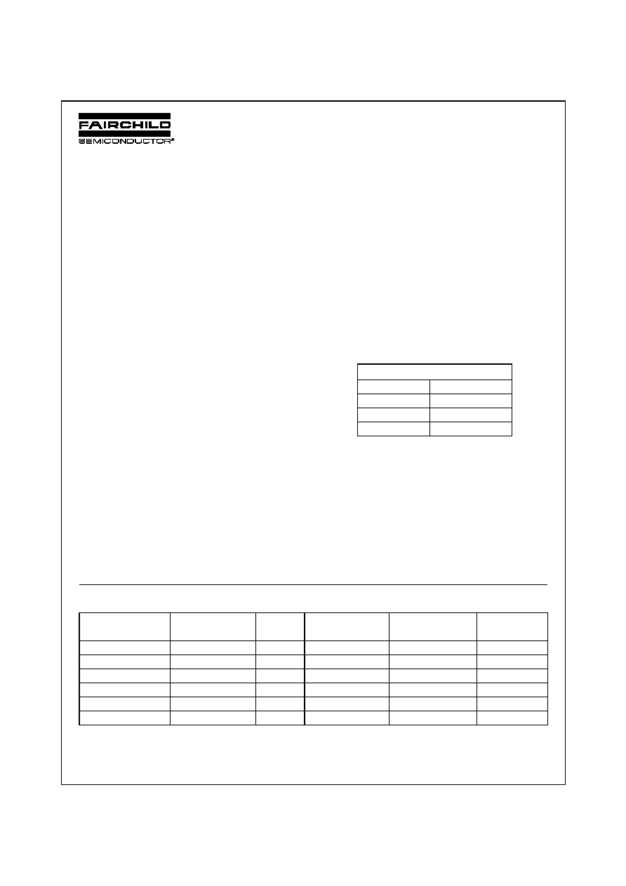
Table 1. Maximum Output Power
Note:
1. Maximum practical continuous power in an open
frame design at 50
∞C ambient.
Ordering Information
Note:
2. X : Tape & Reel
OUTPUT POWER TABLE
(1)
PRODUCT
36V
DC
~72V
DC
FS6X0420RJ
14W
FS6X0720RJ
26W
FS6X1220RJ
36W
Part Number
Operating Temp.
Range
Pb-Free
Package Packing
Method
Marking
Code
FS6X0420RJ
-25
∞C to +85∞C
Yes
D2-Pak-6L
Tube
6X0420R
FS6X0720RJ
-25
∞C to +85∞C
Yes
D2-Pak-6L
Tube
6X0720R
FS6X1220RJ
-25
∞C to +85∞C
Yes
D2-Pak-6L
Tube
6X1220R
FS6X0420RJX
-25
∞C to +85∞C
Yes
D2-Pak-6L
Tape & Reel
6X0420R
FS6X0720RJX
-25
∞C to +85∞C
Yes
D2-Pak-6L
Tape & Reel
6X0720R
FS6X1220RJX
(2)
-25
∞C to +85∞C
Yes
D2-Pak-6L
Tape & Reel
6X1220R

2
www.fairchildsemi.com
FS6X0420RJ/ FS6X0720RJ/ FS6X1220RJ Rev. 1.0.1
FS6
X
04
20
RJ
/ FS
6X0
7
2
0
RJ/
FS6X
12
20RJ
Fa
irchil
d Powe
r Sw
itch (FPS
TM)
Typical Application Diagram
Figure 1. Typical Flyback Application
Internal Block Diagram
Figure 2. Functional Block Diagram of FS6X-Series
Drain
GND
Vfb
Vcc
PWM
DC
IN
DC
OUT
L/S
V
SL
V
LU
9V/15V
3
1
2
4
6
Vref
Line
UVLO
Enable
Internal
Bias
S
Q
Q
R
OSC
V
CC
V
ref
I
delay
I
FB
V
SD
TSD
V
OVP
V
CC
Line UVLO
S
Q
R
R
28R
V
CC
Good
V
CC
Drain
Line
Sense
FB
GND
Gate
Driver
5
N.C
Q
V
CC
Good

3
www.fairchildsemi.com
FS6X0420RJ/ FS6X0720RJ/ FS6X1220RJ Rev. 1.0.1
FS6
X
04
20
RJ
/ FS
6X0
7
2
0
RJ/
FS6X
12
20RJ
Fa
irchil
d Powe
r Sw
itch (FPS
TM)
Pin Assignments
Figure 3. Pin Configuration (Top View)
Pin Definitions
Pin Number
Pin Name
Pin Function Description
1
Drain
This pin is the high voltage power SenseFET drain connection.
2
GND
This pin is the control ground and the SenseFET source.
3
Vcc
This pin is the positive supply input. This pin provides internal operating current for both
start-up and steady-state operation.
4
Feedback
(FB)
This pin is internally connected to the inverting input of the PWM comparator. The collec-
tor of an opto-coupler is typically tied to this pin. For stable operation, a capacitor should
be placed between this pin and GND. If the voltage of this pin reaches 7.5V, the over load
protection is activated resulting in shutdown of the IC.
5
N.C.
This pin is not connected.
6
Line Sense (LS)
According to the voltage of this pin, three operation modes are defined: normal operation
mode, line under voltage lock out mode, and sleep mode. If the voltage of this pin is
smaller than 2.55V, the IC goes into the line under voltage lock out, stopping switching
operation. If the voltage of this pin is smaller than 1.8V, the IC enters into sleep mode.
During sleep mode, reference voltage generation circuit including the shunt regulator is
disabled and only 300uA operation current is required.
6. Line Sense
5. N.C.
4. Vfb
3. Vcc
2. GND
1. Drain
D2-PAK-6L

4
www.fairchildsemi.com
FS6X0420RJ/ FS6X0720RJ/ FS6X1220RJ Rev. 1.0.1
FS6
X
04
20
RJ
/ FS
6X0
7
2
0
RJ/
FS6X
12
20RJ
Fa
irchil
d Powe
r Sw
itch (FPS
TM)
Absolute Maximum Ratings
(Ta=25
∞C, unless otherwise specified
.
)
Note:
1. Repetitive rating: Pulse width limited by maximum junction temperature.
Thermal Impedance
Note:
1. Infinite cooling condition - Refer to the SEMI G30-88.
Parameter
Symbol
Value
Unit
Drain-source Voltage
V
DSS
200
V
Pulsed Drain Current (Tc=25
∞C)
(1)
I
DM
FS6X0420RJ
10.2
A
FS6X0720RJ
16.2
FS6X1220RJ
23.7
Continuous Drain Current (Tc=25
∞C) I
D
FS6X0420RJ
3.4
A (rms)
FS6X0720RJ
5.4
FS6X1220RJ
12.4
Continuous Drain Current (Tc=100
∞C) I
D
FS6X0420RJ
2.1
A (rms)
FS6X0720RJ
3.4
FS6X1220RJ
7.9
Supply Voltage
V
CC
35
V
Input Voltage Range
V
FB
-0.3 to V
CC
V
Total Power Dissipation (Tc=25
∞C)
P
D
FS6X0420RJ
43
W
FS6X0720RJ
54
FS6X1220RJ
125
Operating Junction Temperature
T
j
Internally limited
∞C
Operating Ambient Temperature
T
A
-25 to +85
∞C
Storage Temperature Range
T
STG
-55 to +150
∞C
Parameter
Symbol
Value
Unit
Junction-to-Ambient Thermal
JA
-
∞C/W
Junction-to-Case Thermal
(1)
JC
FS6X0420RJ
2.9
∞C/W
FS6X0720RJ
2.3
FS6X1220RJ
1.0

5
www.fairchildsemi.com
FS6X0420RJ/ FS6X0720RJ/ FS6X1220RJ Rev. 1.0.1
FS6
X
04
20
RJ
/ FS
6X0
7
2
0
RJ/
FS6X
12
20RJ
Fa
irchil
d Powe
r Sw
itch (FPS
TM)
Electrical Characteristics
(Ta=25
∞C, unless otherwise specified.)
Notes:
1. Pulse test: Pulse width
300S, duty 2%.
2. These parameters, although guaranteed at the design, are not tested in mass production.
3. These parameters indicate the inductor current.
Parameter Symbol
Condition
Min.
Typ
.
Max.
Unit
SENSE FET SECTION
Drain Source Breakdown Voltage
BV
DSS
V
GS
= 0V, I
D
= 250
A
200
220
-
V
Zero Gate Voltage Drain Current
I
DSS
V
DS
= 200V, V
GS
= 0V
-
-
250
A
V
DS
= 160V
V
GS
= 0V, T
C
= 125
∞C
-
-
250
A
Static Drain Source on Resistance
(1)
R
DS(ON)
FS6X0420RJ
V
GS
= 10V, I
D
= 2.5A
-
1.2
1.5
FS6X0720RJ
-
0.64
0.75
FS6X1220RJ
-
0.24
0.30
Output Capacitance
C
OSS
FS6X0420RJ
V
GS
= 0V
V
DS
= 25V, f = 1MHz
-
32
45
pF
FS6X0720RJ
-
49
65
FS6X1220RJ
-
125
160
CONTROL SECTION
Initial Frequency
F
OSC
-
270
300
330
kHz
Voltage Stability
F
STABLE
12V
Vcc 23V
0
1
3
%
Temperature Stability
(2)
F
OSC
-25
∞C Ta 85∞C
0
±5
±10
%
Maximum Duty Cycle
D
MAX
-
72
80
88
%
Minimum Duty Cycle
D
MIN
-
-
-
0
%
Start Threshold Voltage
V
START
V
FB
= GND
14
15
16
V
Stop Threshold Voltage
V
STOP
V
FB
= GND
8
9
10
V
Feedback Source Current
I
FB
V
FB
= GND
0.7
0.9
1.1
mA
PROTECTION SECTION
Peak Current Limit
(3)
I
Limit
FS6X0420RJ
-
1.2
1.4
1.6
A
FS6X0720RJ
2.3
2.7
3.1
FS6X1220RJ
2.8
3.2
3.6
Over Voltage Protection
V
OVP
V
CC
> 6.9V
23
25
27
V
Thermal Shutdown Temperature
(2)
T
SD
-
140
160
-
∞C
Shutdown Feedback Voltage
V
SD
V
FB
6.9V
6.9
7.5
8.1
V
Shutdown Delay Current
I
DELAY
V
FB
= 5V
4.0
5.0
6.0
A


