 | –≠–ª–µ–∫—Ç—Ä–æ–Ω–Ω—ã–π –∫–æ–º–ø–æ–Ω–µ–Ω—Ç: FSA3157 | –°–∫–∞—á–∞—Ç—å:  PDF PDF  ZIP ZIP |

© 2003 Fairchild Semiconductor Corporation
DS500326
www.fairchildsemi.com
January 2000
Revised June 2003
NC7SB3157
∑
FSA
3
157 T
i
nyLogi
c
Low V
o
l
t
age
UHS SPDT
A
n
a
l
og
Sw
i
t
c
h or
2:
1 Mul
t
i
p
le
xer/
D
em
ul
ti
pl
exer
Bus
Swi
t
ch
NC7SB3157 ∑ FSA3157
TinyLogic
Low Voltage UHS SPDT Analog Switch
or 2:1 Multiplexer/Demultiplexer Bus Switch
General Description
The NC7SB3157 or FSA3157 is a high performance, sin-
gle-pole/double-throw (SPDT) Analog Switch or 2:1 Multi-
plexer/Demultiplexer Bus Switch from Fairchild's Ultra High
Speed Series of TinyLogic
. The device is fabricated with
advanced sub-micron CMOS technology to achieve high
speed enable and disable times and low On Resistance.
The break before make select circuitry prevents disruption
of signals on the B Port due to both switches temporarily
being enabled during select pin switching. The device is
specified to operate over the 1.65 to 5.5V V
CC
operating
range. The control input tolerates voltages up to 5.5V inde-
pendent of the V
CC
operating range.
Features
s
Useful in both analog and digital applications
s
Space saving SC70 6-lead surface mount package
s
Ultra small MicroPak
leadless package
s
Low On Resistance;
<
10
on typ @ 3.3V V
CC
s
Broad V
CC
operating range; 1.65V to 5.5V
s
Rail-to-Rail signal handling
s
Power down high impedance control input
s
Overvoltage tolerance of control input to 7.0V
s
Break before make enable circuitry
s
250 MHz - 3dB bandwidth
Ordering Code:
TinyLogic
is a registered trademark and MicroPak
is a trademark of Fairchild Semiconductor Corporation.
Order
Number
Package
Number
Product Code
Top Mark
Package Description
Supplied As
NC7SB3157P6X
MAA06A
B7A
6-Lead SC70, EIAJ SC88, 1.25mm Wide
3k Units on Tape and Reel
NC7SB3157L6X
MAC06A
BB
6-Lead MicroPak, 1.0mm Wide
5k Units on Tape and Reel
FSA3157P6X
MAA06A
B7A
6-Lead SC70, EIAJ SC88, 1.25mm Wide
3k Units on Tape and Reel
FSA3157L6X
MAC06A
BB
6-Lead MicroPak, 1.0mm Wide
5k Units on Tape and Reel

www.fairchildsemi.com
2
NC7SB3157
∑
FSA3157
Logic Symbol
Analog Symbol
Function Table
H
=
HIGH Logic Level
L
=
LOW Logic Level
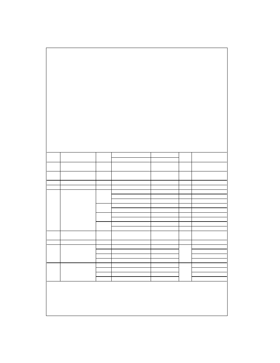
Pin Descriptions
Connection Diagrams
Pin Assignments for SC70
(Top View)
Pin One Orientation Diagram
AAA
=
Product Code Top Mark - see ordering code.
Note: Orientation of Top Mark determines Pin One location. Read the top
product code mark left to right, Pin One is the lower left pin (see diagram).
Pad Assignments for MicroPak
(Top Thru View)
Input (S)
Function
L
B
0
Connected to A
H
B
1
Connected to A
Pin Names
Description
A, B
0
, B
1
Data Ports
S
Control Input
3
www.fairchildsemi.com
NC7SB3157
∑
FSA
3
157
Absolute Maximum Ratings
(Note 1)
Recommended Operating
Conditions
(Note 3)
Note 1: Absolute maximum ratings are DC values beyond which the device
may be damaged or have its useful life impaired. The datasheet specifica-
tions should be met, without exception, to ensure that the system design is
reliable over its power supply, temperature, and output/input loading vari-
ables. Fairchild does not recommend operation outside datasheet specifi-
cations.
Note 2: The input and output negative voltage ratings may be exceeded if
the input and output diode current ratings are observed.
Note 3: Control input must be held HIGH or LOW, it must not float.
DC Electrical Characteristics
Supply Voltage (V
CC
)
-
0.5V to
+
7.0V
DC Switch Voltage (V
S
) (Note 2)
-
0.5V to V
CC
+
0.5V
DC Input Voltage (V
IN
) (Note 2)
-
0.5V to
+
7.0V
DC Input Diode Current (I
IK
)
@ (I
IK
) V
IN
<
0V
-
50 mA
DC Output Current (I
OUT
)
128 mA
DC V
CC
or Ground Current (I
CC
/I
GND
)
±
100 mA
Storage Temperature Range (T
STG
)
-
65
∞
C to
+
150
∞
C
Junction Temperature under Bias (T
J
)
150
∞
C
Junction Lead Temperature (T
L
)
(Soldering, 10 seconds)
260
∞
C
Power Dissipation (P
D
) @
+
85
∞
C
180 mW
Supply Voltage Operating (V
CC
)
1.65V to 5.5V
Control Input Voltage (V
IN
)
0V to V
CC
Switch Input Voltage (V
IN
)
0V to V
CC
Output Voltage (V
OUT
)
0V to V
CC
Operating Temperature (T
A
)
-
40
∞
C to
+
85
∞
C
Input Rise and Fall Time (t
r
, t
f
)
Control Input V
CC
=
2.3V - 3.6V
0 ns/V to 10 ns/V
Control Input V
CC
=
4.5V - 5.5V
0 ns/V to 5 ns/V
Thermal Resistance (
JA
)
350
∞
C/W
Symbol
Parameter
V
CC
T
A
=
+
25
∞
C
T
A
=
-
40
∞
C to
+
85
∞
C
Units
Conditions
(V)
Min
Typ
Max
Min
Max
V
IH
HIGH Level
1.65
-
1.95 0.75 V
CC
0.75 V
CC
V
Input Voltage
2.3
-
5.5
0.7 V
CC
0.7 V
CC
V
IL
LOW Level
1.65
-
1.95
0.25 V
CC
0.25 V
CC
V
Input Voltage
2.3
-
5.5
0.3 V
CC
0.3 V
CC
I
IN
Input Leakage Current
0
-
5.5
±
0.05
±
0.1
±
1
µ
A
0
V
IN
5.5V
I
OFF
OFF State Leakage Current
1.65
-
5.5
±
0.05
±
0.1
±
1
µ
A
0
A, B
V
CC
R
ON
Switch On Resistance
4.5
3
7
7
V
IN
=
0V, I
O
=
30 mA
(Note 4)
5
12
12
V
IN
=
2.4V, I
O
=
-
30 mA
7
15
15
V
IN
=
4.5V, I
O
=
-
30 mA
3.0
4
9
9
V
IN
=
0V, I
O
=
24 mA
10
20
20
V
IN
=
3V, I
O
=
-
24 mA
2.3
5
12
12
V
IN
=
0V, I
O
=
8 mA
13
30
30
V
IN
=
2.3V, I
O
=
-
8 mA
1.65
6.5
20
20
V
IN
=
0V, I
O
=
4 mA
17
50
50
V
IN
=
1.65V, I
O
=
-
4 mA
I
CC
Quiescent Supply Current
5.5
1
10
µ
A
V
IN
=
V
CC
or GND
All Channels ON or OFF
I
OUT
=
0
Analog Signal Range
V
CC
0
V
CC
0
V
CC
V
R
RANGE
On Resistance
4.5
25
I
A
=
-
30 mA, 0
V
Bn
V
CC
Over Signal Range
3.0
50
I
A
=
-
24 mA, 0
V
Bn
V
CC
(Note 4)(Note 8)
2.3
100
I
A
=
-
8 mA, 0
V
Bn
V
CC
1.65
300
I
A
=
-
4 mA, 0
V
Bn
V
CC
R
ON
On Resistance Match
4.5
0.15
I
A
=
-
30 mA, V
Bn
=
3.15
Between Channels
3.0
0.2
I
A
=
-
24 mA, V
Bn
2.1
(Note 4)(Note 5)(Note 6)
2.3
0.5
I
A
=
-
8 mA, V
Bn
=
1.6
1.65
0.5
I
A
=
-
4 mA, V
Bn
=
1.15
www.fairchildsemi.com
4
NC7SB3157
∑
FSA3157
DC Electrical Characteristics
(Continued)
Note 4: Measured by the voltage drop between A and B pins at the indicated current through the switch. On Resistance is determined by the lower of the
voltages on the two (A or B Ports).
Note 5: Parameter is characterized but not tested in production.
Note 6:
R
ON
=
R
ON
max
-
R
ON
min measured at identical V
CC
, temperature and voltage levels.
Note 7: Flatness is defined as the difference between the maximum and minimum value of On Resistance over the specified range of conditions.
Note 8: Guaranteed by Design.
AC Electrical Characteristics
Note 9: Guaranteed by Design.
Note 10: This parameter is guaranteed by design but not tested. The bus switch contributes no propagation delay other than the RC delay of the On Resis-
tance of the switch and the 50 pF load capacitance, when driven by an ideal voltage source (zero output impedance).
Note 11: Off Isolation
=
20 log
10
[V
A
/ V
Bn
]
Symbol
Parameter
V
CC
T
A
=
+
25
∞
C
T
A
=
-
40
∞
C to
+
85
∞
C
Units
Conditions
(V)
Min
Typ
Max
Min
Max
R
flat
On Resistance Flatness
5.0
6
I
A
=
-
30 mA, 0
V
Bn
V
CC
(Note 4)(Note 5)(Note 7)
3.3
12
I
A
=
-
24 mA, 0
V
Bn
V
CC
2.5
28
I
A
=
-
8 mA, 0
V
Bn
V
CC
1.8
125
I
A
=
-
4 mA, 0
V
Bn
V
CC
Symbol
Parameter
V
CC
T
A
=
+
25
∞
C
T
A
=
-
40
∞
C to
+
85
∞
C
Units
Conditions
Figure
(V)
Min
Typ
Max
Min
Max
Number
t
PHL
Propagation Delay
1.65
-
1.95
3.5
3.5
ns
V
I
=
OPEN
Figures
1, 2
t
PLH
Bus to Bus
2.3
-
2.7
1.2
1.2
(Note 10)
3.0
-
3.6
0.8
0.8
4.5
-
5.5
0.3
0.3
t
PZL
Output Enable Time
1.65
-
1.95
7
23
7
24
ns
Figures
1, 2
t
PZH
Turn on Time
2.3
-
2.7
3.5
13
3.5
14
V
I
=
2 x V
CC
for t
PZL
(A to B
n
)
3.0
-
3.6
2.5
6.9
2.5
7.6
V
I
=
0V for t
PZH
4.5
-
5.5
1.7
5.2
1.7
5.7
t
PLZ
Output Disable Time
1.65
-
1.95
3
12.5
3
13
ns
Figures
1, 2
t
PHZ
Turn Off Time
2.3
-
2.7
2
7
2
7.5
V
I
=
2 x V
CC
for t
PLZ
(A Port to B Port)
3.0
-
3.6
1.5
5
1.5
5.3
V
I
=
0V for t
PHZ
4.5
-
5.5
0.8
3.5
0.8
3.8
t
B-M
Break Before Make Time 1.65
-
1.95
0.5
0.5
ns
Figure 3
(Note 9)
2.3
-
2.7
0.5
0.5
3.0
-
3.6
0.5
0.5
4.5
-
5.5
0.5
0.5
Q
Charge Injection (Note 9)
5.0
7
pC
C
L
=
0.1 nF, V
GEN
=
0V
Figure 4
3.3
3
R
GEN
=
0
OIRR
Off Isolation (Note 11)
1.65
-
5.5
-
57
dB
R
L
=
50
Figure 5
f
=
10MHz
Xtalk
Crosstalk
1.65
-
5.5
-
54
dB
R
L
=
50
Figure 6
f
=
10MHz
BW
-
3dB Bandwidth
1.65
-
5.5
250
MHz
R
L
=
50
Figure 9
THD
Total Harmonic Distortion
5
.011
%
R
L
=
600
(Note 9)
0.5 V
P-P
f
=
600 Hz to 20 KHz
5
www.fairchildsemi.com
NC7SB3157
∑
FSA
3
157
Capacitance
(Note 12)
Note 12: T
A
=
+
25
∞
C, f
=
1 MHz, Capacitance is characterized but not tested in production.
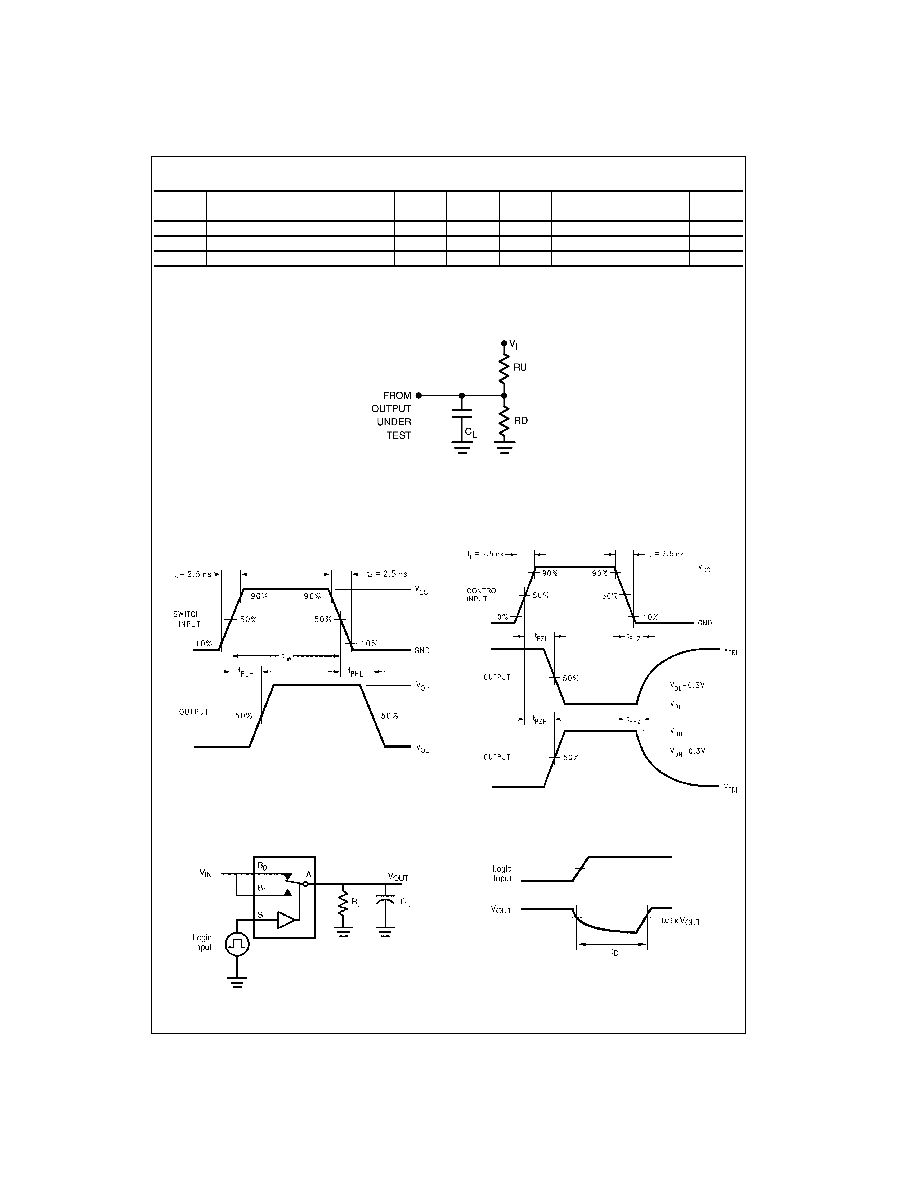
AC Loading and Waveforms
Note: Input driven by 50
source terminated in 50
Note: C
L
includes load and stray capacitance
Note: Input PRR
=
1.0 MHz; t
W
=
500 ns
FIGURE 1. AC Test Circuit
FIGURE 2. AC Waveforms
FIGURE 3. Break Before Make Interval Timing
Symbol
Parameter
Typ
Max
Units
Conditions
Figure
Number
C
IN
Control Pin Input Capacitance
2.3
pF
V
CC
=
0V
C
IO-B
B Port Off Capacitance
6.5
pF
V
CC
=
5.0V
Figure 7
C
IOA-ON
A Port Capacitance When Switch Is Enabled
18.5
pF
V
CC
=
5.0V
Figure 8

www.fairchildsemi.com
6
NC7SB3157
∑
FSA3157
AC Loading and Waveforms
(Continued)
FIGURE 4. Charge Injection Test
FIGURE 5. Off Isolation
FIGURE 6. Crosstalk
FIGURE 7. Channel Off Capacitance
FIGURE 8. Channel On Capacitance
FIGURE 9. Bandwidth
7
www.fairchildsemi.com
NC7SB3157
∑
FSA
3
157
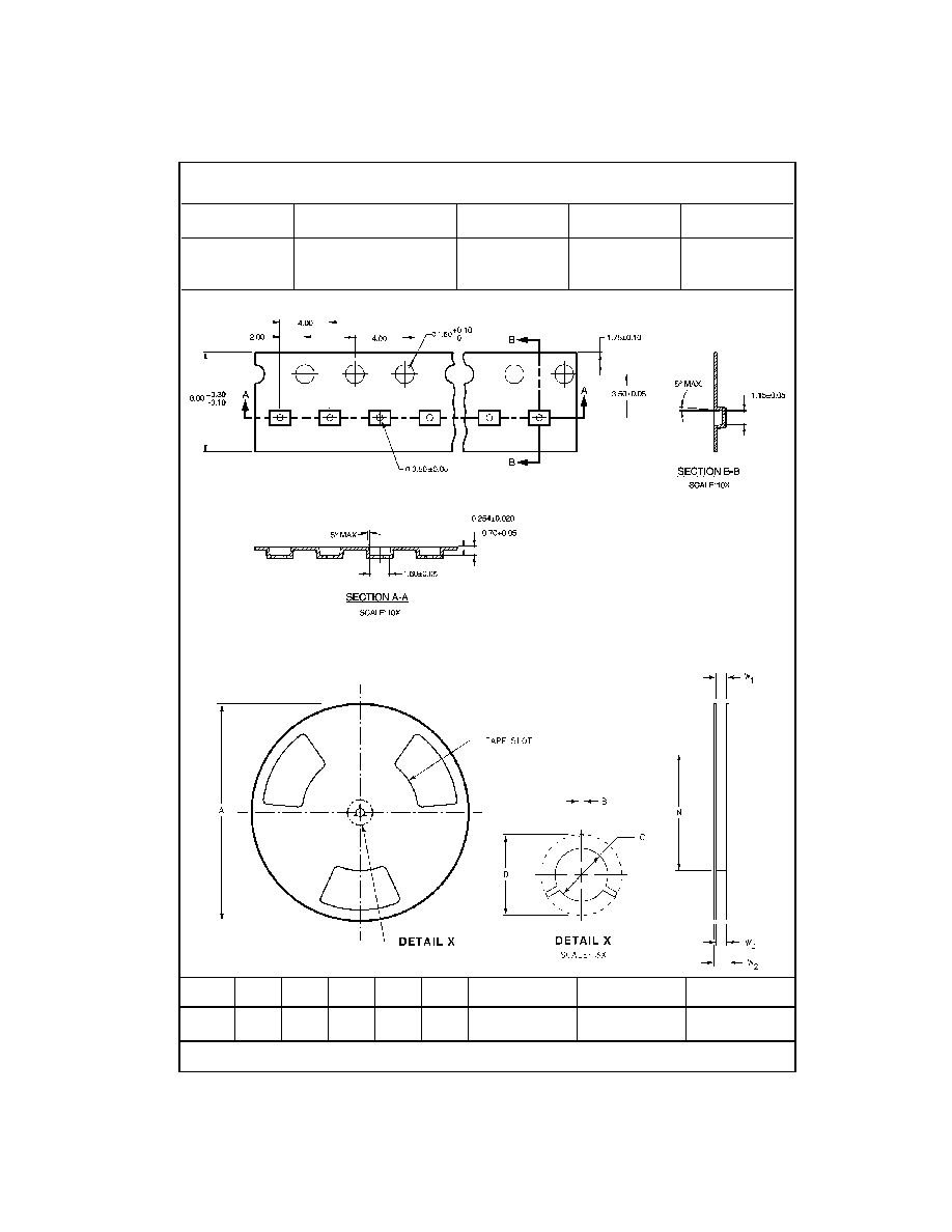
Tape and Reel Specification
TAPE FORMAT for SC70
TAPE DIMENSIONS inches (millimeters)
Package
Tape
Number
Cavity
Cover Tape
Designator
Section
Cavities
Status
Status
Leader (Start End)
125 (typ)
Empty
Sealed
P6X
Carrier
3000
Filled
Sealed
Trailer (Hub End)
75 (typ)
Empty
Sealed
Package
Tape Size
DIM A
DIM B
DIM F
DIM K
o
DIM P1
DIM W
SC70-6
8 mm
0.093
0.096
0.138
±
0.004 0.053
±
0.004
0.157
0.315
±
0.004
(2.35)
(2.45)
(3.5
±
0.10)
(1.35
±
0.10)
(4)
(8
±
0.1)
www.fairchildsemi.com
8
NC7SB3157
∑
FSA3157
Tape and Reel Specification
(Continued)
TAPE FORMAT for MicroPak
TAPE DIMENSIONS inches (millimeters)
REEL DIMENSIONS inches (millimeters)
Package
Tape
Number
Cavity
Cover Tape
Designator
Section
Cavities
Status
Status
Leader (Start End)
125 (typ)
Empty
Sealed
L6X
Carrier
5000
Filled
Sealed
Trailer (Hub End)
75 (typ)
Empty
Sealed
Tape
Size
A
B
C
D
N
W1
W2
W3
8 mm
7.0
0.059
0.512
0.795
2.165
0.331
+
0.059/
-
0.000
0.567
W1
+
0.078/
-
0.039
(177.8)
(1.50)
(13.00)
(20.20)
(55.00)
(8.40
+
1.50/
-
0.00)
(14.40)
(W1
+
2.00/
-
1.00)
9
www.fairchildsemi.com
NC7SB3157
∑
FSA
3
157
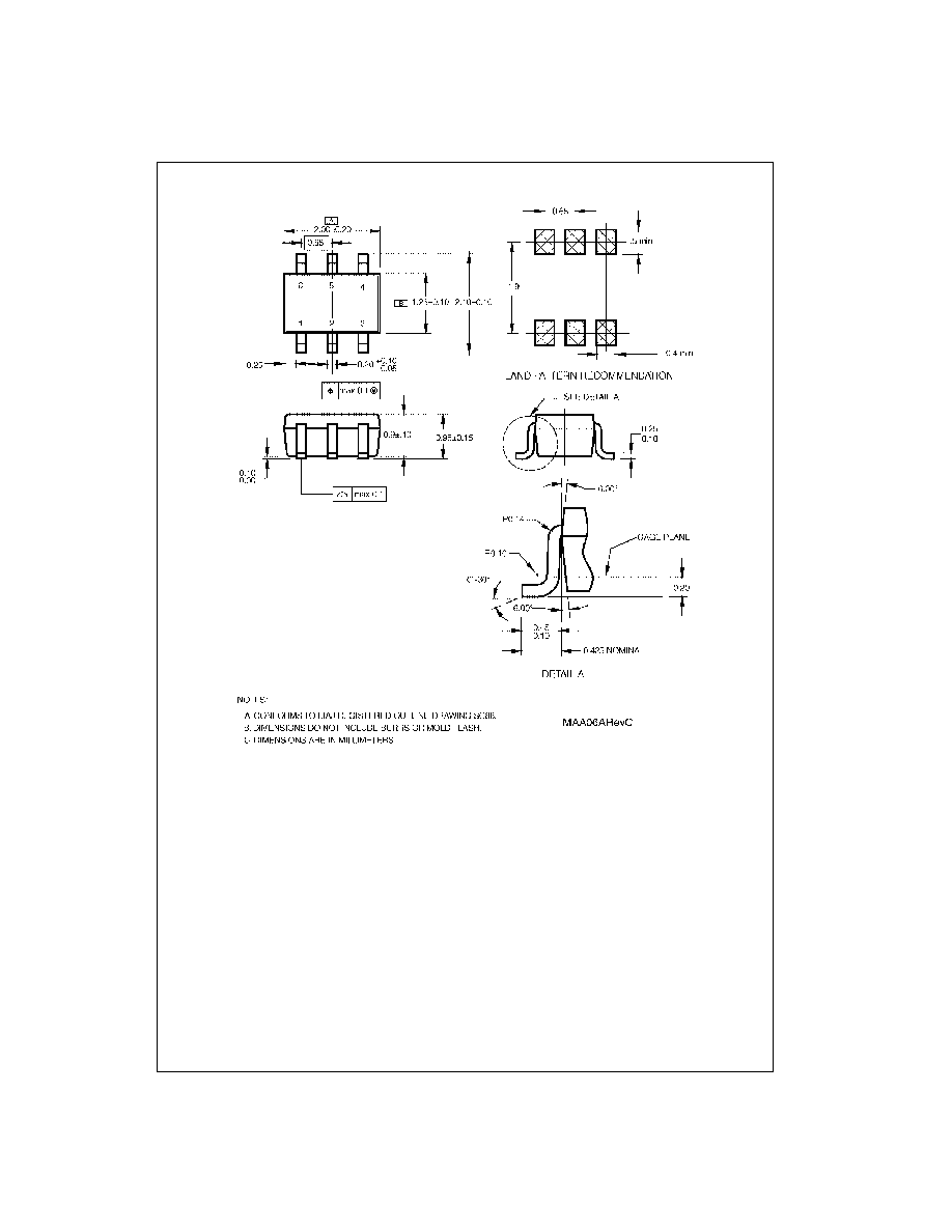
Physical Dimensions
inches (millimeters) unless otherwise noted
6-Lead SC70, EIAJ SC88, 1.25mm Wide
Package Number MAA06A
www.fairchildsemi.com
10
NC7SB3157
∑
FSA3157
T
i
ny
Logic
Low
V
o
lt
age UH
S SPDT
Anal
og S
w
i
t
ch or 2:
1
Mul
t
i
p
lexe
r/Demul
t
i
p
lexe
r B
u
s
Sw
i
t
c
h
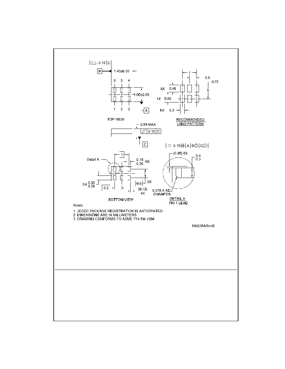
Physical Dimensions
inches (millimeters) unless otherwise noted (Continued)
6-Lead MicroPak, 1.0mm Wide
Package Number MAC06A
Fairchild does not assume any responsibility for use of any circuitry described, no circuit patent licenses are implied and
Fairchild reserves the right at any time without notice to change said circuitry and specifications.
LIFE SUPPORT POLICY
FAIRCHILD'S PRODUCTS ARE NOT AUTHORIZED FOR USE AS CRITICAL COMPONENTS IN LIFE SUPPORT
DEVICES OR SYSTEMS WITHOUT THE EXPRESS WRITTEN APPROVAL OF THE PRESIDENT OF FAIRCHILD
SEMICONDUCTOR CORPORATION. As used herein:
1. Life support devices or systems are devices or systems
which, (a) are intended for surgical implant into the
body, or (b) support or sustain life, and (c) whose failure
to perform when properly used in accordance with
instructions for use provided in the labeling, can be rea-
sonably expected to result in a significant injury to the
user.
2. A critical component in any component of a life support
device or system whose failure to perform can be rea-
sonably expected to cause the failure of the life support
device or system, or to affect its safety or effectiveness.
www.fairchildsemi.com