
© 2002 Fairchild Semiconductor Corporation
DS500805
www.fairchildsemi.com
December 2002
Revised December 2002
F
S
A
3
35
7
L
o
w
V
o
lta
g
e
S
P
3
T
A
n
a
l
og
S
w
i
t
c
h
(
3
:1
M
u
lt
ip
l
e
xe
r
/
D
e
m
u
lt
ip
l
e
x
e
r
)
FSA3357
Low Voltage SP3T Analog Switch
(3:1 Multiplexer/Demultiplexer)
General Description
The FSA3357 is a high performance, single-pole/triple-
throw (SP3T) Analog Switch or 3:1 Multiplexer/Demulti-
plexer. The device is fabricated with advanced sub-micron
CMOS technology to achieve high speed enable and dis-
able times and low On Resistance. The break before make
select circuitry prevents disruption of signals on the B
0
, B
1
,
or B
2
Ports due to the switches temporarily being enabled
during select pin switching. The device is specified to oper-
ate over the 1.65 to 5.5V V
CC
operating range. The control
input tolerates voltages up to 5.5V independent of the V
CC
operating range.
Features
s
Useful in both analog and digital applications
s
Space saving US8 8-lead surface mount package
s
Low On Resistance;
<
9
on typ @ 3.3V V
CC
s
Broad V
CC
operating range; 1.65V to 5.5V
s
Rail-to-Rail signal handling
s
Power down high impedance control input
s
Overvoltage tolerance of control input to 7.0V
s
Break before make enable circuitry
s
250 MHz - 3dB bandwidth
Ordering Code:
Analog Symbol
Function Table
Connection Diagram
(Top View)
Pin Descriptions
Product
Package Description
Supplied As
Order
Package
Code
Number
Number Top Mark
FSA3357K8X
MAB08A
A357
8-Lead US8, JEDEC MO-187, Variation CA 3.1mm Wide 3k Units on Tape and Reel
S
1
S
2
Function
0
0
No Connection
1
0
B
0
Connected to A
0
1
B
1
Connected to A
1
1
B
2
Connected to A
Pin Names
Description
A
1
, B
0
, B
1
, B
2
Data Ports
S
1
, S
2
Control Input

www.fairchildsemi.com
2
FSA3357
Absolute Maximum Ratings
(Note 1)
Recommended Operating
Conditions
(Note 3)
Note 1: Absolute maximum ratings are DC values beyond which the device
may be damaged or have its useful life impaired. The datasheet specifica-
tions should be met, without exception, to ensure that the system design is
reliable over its power supply, temperature, and output/input loading vari-
ables. Fairchild does not recommend operation outside datasheet specifi-
cations.
Note 2: The input and output negative voltage ratings may be exceeded if
the input and output diode current ratings are observed.
Note 3: Control inputs must be held HIGH or LOW, they must not float.
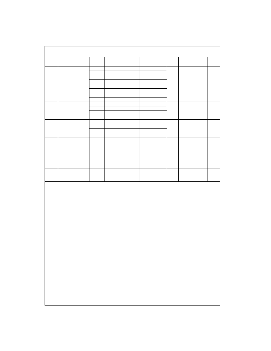
DC Electrical Characteristics
Note 4: Measured by the voltage drop between A and B
n
pins at the indicated current through the switch. On Resistance is determined by the lower of the
voltages on the two (A or B
n
Ports).
Note 5: Parameter is characterized but not tested in production.
Note 6:
R
ON
=
R
ON
max
-
R
ON
min measured at identical V
CC
, temperature and voltage levels.
Note 7: Flatness is defined as the difference between the maximum and minimum value of On Resistance over the specified range of conditions.
Supply Voltage (V
CC
)
-
0.5V to
+
7.0V
DC Switch Voltage (V
S
) (Note 2)
-
0.5V to V
CC
+
0.5V
DC Input Voltage (V
IN
) (Note 2)
-
0.5V to
+
7.0V
DC Input Diode Current (I
IK
)
@ (I
IK
) V
IN
<
0V
-
50 mA
DC Output Current (I
OUT
)
128 mA
DC V
CC
or Ground Current (I
CC
/I
GND
)
±
100 mA
Storage Temperature Range (T
STG
)
-
65
∞
C to
+
150
∞
C
Junction Temperature under Bias (T
J
)
150
∞
C
Junction Lead Temperature (T
L
)
(Soldering, 10 seconds)
260
∞
C
Power Dissipation (P
D
) @
+
85
∞
C
180 mW
Supply Voltage Operating (V
CC
)
1.65V to 5.5V
Control Input Voltage (V
IN
)
0V to V
CC
Switch Input Voltage (V
IN
)
0V to V
CC
Output Voltage (V
OUT
)
0V to V
CC
Operating Temperature (T
A
)
-
40
∞
C to
+
85
∞
C
Input Rise and Fall Time (t
r
, t
f
)
Control Input V
CC
=
2.3V - 3.6V
0 ns/V to 10 ns/V
Control Input V
CC
=
4.5V - 5.5V
0 ns/V to 5 ns/V
Thermal Resistance (
JA
)
250
∞
C/W
Symbol
Parameter
V
CC
T
A
=
+
25
∞
C
T
A
=
-
40
∞
C to
+
85
∞
C
Units
Conditions
(V)
Min
Typ
Max
Min
Max
V
IH
HIGH Level
1.65
-
1.95 0.75 V
CC
0.75 V
CC
V
Input Voltage
2.3
-
5.5
0.7 V
CC
0.7 V
CC
V
IL
LOW Level
1.65
-
1.95
0.25 V
CC
0.25 V
CC
V
Input Voltage
2.3
-
5.5
0.3 V
CC
0.3 V
CC
I
IN
Input Leakage Current
0
-
5.5
±
0.1
±
1.0
µ
A
0
V
IN
5.5V
I
OFF
OFF State Leakage Current
1.65
-
5.5
±
0.1
±
1.0
µ
A
0
A, B
n
V
CC
R
ON
Switch On Resistance
4.5
5.0
7.0
7.0
V
IN
=
0V, I
O
=
30 mA
(Note 4)
6.0
12.0
12.0
V
IN
=
2.4V, I
O
=
-
30 mA
7.0
15.0
15.0
V
IN
=
4.5V, I
O
=
-
30 mA
3.0
6.5
9.0
9.0
V
IN
=
0V, I
O
=
24 mA
9.0
20.0
20.0
V
IN
=
3V, I
O
=
-
24 mA
2.3
8.0
12.0
12.0
V
IN
=
0V, I
O
=
8 mA
11.0
30.0
30.0
V
IN
=
2.3V, I
O
=
-
8 mA
1.65
10.0
20.0
20.0
V
IN
=
0V, I
O
=
4 mA
17.0
50.0
50.0
V
IN
=
1.65V, I
O
=
-
4 mA
I
CC
Quiescent Supply Current
5.5
1.0
10.0
µ
A
V
IN
=
V
CC
or GND
All Channels ON or OFF
I
OUT
=
0
ASR
Analog Signal Range
V
CC
0.0
V
CC
0.0
V
CC
V
R
ON
On Resistance Match
4.5
0.15
I
A
=
-
30 mA, V
Bn
=
3.15
Between Channels
3.0
0.22
I
A
=
-
24 mA, V
Bn
=
2.1
(Note 4)(Note 5)(Note 6)
2.3
0.31
I
A
=
-
8 mA, V
Bn
=
1.6
1.65
0.62
I
A
=
-
4 mA, V
Bn
=
1.15
R
flat
On Resistance Flatness
5.0
6.0
I
A
=
-
30 mA, 0
V
Bn
V
CC
(Note 4)(Note 5)(Note 7)
3.3
12.0
I
A
=
-
24 mA, 0
V
Bn
V
CC
2.5
40.0
I
A
=
-
8 mA, 0
V
Bn
V
CC
1.8
140.0
I
A
=
-
4 mA, 0
V
Bn
V
CC
3
www.fairchildsemi.com
FSA33
5
7
AC Electrical Characteristics
Note 8: This parameter is guaranteed by design but not tested. The bus switch contributes no propagation delay other than the RC delay of the
On Resistance of the switch and the 50 pF load capacitance, when driven by an ideal voltage source (zero output impedance).
Note 9: Guaranteed by Design.
Note 10: Off Isolation
=
20 log
10
[V
A
/ V
Bn
]
Symbol
Parameter
V
CC
T
A
=
+
25
∞
C
T
A
=
-
40
∞
C to
+
85
∞
C
Units
Conditions
Figure
(V)
Min
Typ
Max
Min
Max
Number
t
PHL
Propagation Delay
1.65
-
1.95
2.0
ns
V
I
=
OPEN
Figures
1, 2
t
PLH
Bus to Bus
2.3
-
2.7
1.1
(Note 8)
3.0
-
3.6
0.7
4.5
-
5.5
0.4
t
PZL
Output Enable Time
1.65
-
1.95
5.0
32.0
5.0
34.0
ns
Figures
1, 2
t
PZH
Turn on Time
2.3
-
2.7
3.0
15.0
3.0
16.5
V
I
=
2 x V
CC
for t
PZL
(A to B
n
)
3.0
-
3.6
2.0
9.5
2.0
11.0
V
I
=
0V for t
PZH
4.5
-
5.5
1.5
6.5
1.5
7.0
t
PLZ
Output Disable Time
1.65
-
1.95
3.0
14.0
3.0
14.5
ns
Figures
1, 2
t
PHZ
Turn Off Time
2.3
-
2.7
2.0
7.2
2.0
7.8
V
I
=
2 x V
CC
for t
PLZ
(A Port to B
n
Port)
3.0
-
3.6
1.5
5.1
1.5
5.5
V
I
=
0V for t
PHZ
4.5
-
5.5
0.8
3.7
0.8
4.0
t
B-M
Break Before Make Time 1.65
-
1.95
0.5
0.5
ns
Figure 3
(Note 9)
2.3
-
2.7
0.5
0.5
3.0
-
3.6
0.5
0.5
4.5
-
5.5
0.5
0.5
Q
Charge Injection (Note 9)
5.0
3.0
pC
C
L
=
0.1 nF, V
GEN
=
0V
Figure 4
3.3
2.0
R
GEN
=
0
OIRR
Off Isolation (Note 10)
1.65
-
5.5
-
58.0
dB
R
L
=
50
Figure 5
f
=
10MHz
Xtalk
Crosstalk
1.65
-
5.5
-
60.0
dB
R
L
=
50
Figure 6
f
=
10MHz
BW
-
3dB Bandwidth
1.65
-
5.5
250.0
MHz
R
L
=
50
Figure 9
THD
Total Harmonic Distortion
5.0
.01
%
R
L
=
600
(Note 9)
0.5 V
P-P
f
=
600 Hz to 20 KHz

www.fairchildsemi.com
4
FSA3357
Capacitance
(Note 11)
Note 11: T
A
=
+
25
∞
C, f
=
1 MHz, Capacitance is characterized but not tested in production.
AC Loading and Waveforms
Note: Input driven by 50
source terminated in 50
Note: C
L
includes load and stray capacitance
Note: Input PRR
=
1.0 MHz; t
W
=
500 ns
FIGURE 1. AC Test Circuit
FIGURE 2. AC Waveforms
FIGURE 3. Break Before Make Interval Timing
Symbol
Parameter
Typ
Max
Units
Conditions
Figure
Number
C
IN
Control Pin Input Capacitance
2.0
pF
V
CC
=
0V
C
IO-B
B Port Off Capacitance
3.6
pF
V
CC
=
5.0V
Figure 7
C
IOA-ON
A Port Capacitance When Switch Is Enabled
14.5
pF
V
CC
=
5.0V
Figure 8

5
www.fairchildsemi.com
FSA33
5
7
AC Loading and Waveforms
(Continued)
FIGURE 4. Charge Injection Test
FIGURE 5. Off Isolation
FIGURE 6. Crosstalk
FIGURE 7. Channel Off Capacitance
FIGURE 8. Channel On Capacitance
FIGURE 9. Bandwidth