© 2005 Fairchild Semiconductor Corporation
DS500921
www.fairchildsemi.com
May 2005
Revised May 2005
FSA
V
433 Low
V
o
l
t
age
Ul
tr
a
L
o
w
Power High Bandwid
th (5
50M
Hz
) 3-Por
t
3:1 V
i
deo Swit
ch
FSAV433
Low Voltage Ultra Low Power
High Bandwidth (550MHz) 3-Port 3:1 Video Switch
General Description
The FSAV433 is an ultra low power high bandwidth video
switch specially designed for the switching of three analog
video signals, including computer RGB and high definition
YPbPr signals. The wide bandwidth (550MHz) of this
switch allows signal passage with minimum edge and
phase distortion while
85dB non
adjacent channel
crosstalk generates negligible image noise between active
channels. Optimized differential gain and differential
phases maintain the image integrity of video applications
while low On Resistance offers low signal insertion loss.
Features
s
Ground between channels to optimize isolation and
hostile crosstalk
s
85dB non-adjacent channel crosstalk at 10MHz
s
6.5
:
typical On Resistance (R
ON
)
s
3dB bandwidth: 550MHz
s
Low power consumption (1uA max)
Applications
∑ RGB Video Switch in LCD,
plasma and projection displays
∑ DVD-RW, notebook
Ordering Code:
Device also available in Tape and Reel. Specify by appending suffix letter "X" to the ordering code.
Pb-Free package per JEDEC J-STD-020B.
Note 1: DQFN package available in Tape and Reel only.
Order Number Package Number
Package Description
FSAV433BQX
(Preliminary)
(Note 1)
MLP020B
Pb-Free 20-Terminal Depopulated Quad Very-Thin Flat Pack No Leads (DQFN), JEDEC
MO-241, 2.5 x 4.5mm
FSAV433MTC
MTC20
20-Lead Thin Shrink Small Outline Package (TSSOP), JEDEC MO-153, 4.4mm Wide

3
www.fairchildsemi.com
FSA
V
433
Absolute Maximum Ratings
(Note 2)
Recommended Operating
Conditions
(Note 4)
Note 2: The Absolute Maximum Ratings are those values beyond which
the safety of the device cannot be guaranteed. The device should not be
operated at these limits. The parametric values defined in the Electrical
Characteristics tables are not guaranteed at the absolute maximum rating.
The Recommended Operating Conditions tables will define the conditions
for actual device operation.
Note 3: The input and output negative voltage ratings may be exceeded if
the input and output diode current ratings are observed.
Note 4: Unused control inputs must be held HIGH or LOW. They may not
float.
DC Electrical Characteristics
Note 5: Typical values are at T
A
25
q
C
Note 6: Measured by the voltage drop between A and B pins at the indicated current through the switch. On Resistance is determined by the lower of the
voltages on the two (A or B) pins.
Supply Voltage (V
CC
)
0.5V to
4.6V
DC Switch Voltage (V
S
)
0.5V to V
CC
0.05V
DC Input Voltage (V
IN
) (Note 3)
0.5V to
4.6V
DC Input Diode Current (l
IK
) V
IN
0V
50 mA
DC Output (I
OUT
) Sink Current
100 mA
DC V
CC
/GND Current (I
CC
/I
GND
)
r
100 mA
Storage Temperature Range (T
STG
)
65
q
C to
150
q
C
ESD
Human Body Model
7kV
Power Supply Operating (V
CC
)
2.3V to 3.6V
Input Voltage (V
IN
)
0V to V
CC
Free Air Operating Temperature (T
A
)
40
q
C to
85
q
C
Symbol
Parameter
V
CC
(V)
T
A
40
q
C to
85
q
C
Units
Conditions
Min
Typ
(Note 5)
Max
Analog Signal Range
0
2.0
V
V
IK
Clamp Diode Voltage
3.0
1.2
V
I
IN
18 mA
V
IH
HIGH Level Input Voltage
2.3
1.8
V
3.0 - 3.6
2.0
V
IL
LOW Level Input Voltage
2.3
0.7
V
3.0 - 3.6
0.8
I
I
Input Leakage Current
3.6
r
1.0
P
A
0
d
V
IN
d
3.6V
I
OFF
OFF-STATE Leakage Current
3.6
r
1.0
P
A
0
d
A, B
d
V
CC
, See Figure 5
R
ON
Switch On Resistance
2.3
9.0
13.0
:
V
IN
1.0V
(Note 6)
3.0
6.5
9.0
I
ON
13 mA, See Figure 4
2.3
10.0
15.0
:
V
IN
2.0V
3.0
6.5
9.0
I
ON
26 mA, See Figure 4
I
CC
Quiescent Supply Current
3.6
1.0
P
A
V
IN
V
CC
or GND, I
OUT
0
I
CCT
Increase in I
CC
per Control Input
3.6
10.0
uA
One Control Input at 3.0V
Other Inputs at V
CC
or GND
www.fairchildsemi.com
4
FSA
V
433
AC Electrical Characteristics
Note 7: Typical values are at V
CC
3.3V and T
A
25
q
C
Capacitance
Note 8: Typical values are at V
CC
3.3V and T
A
25
q
C
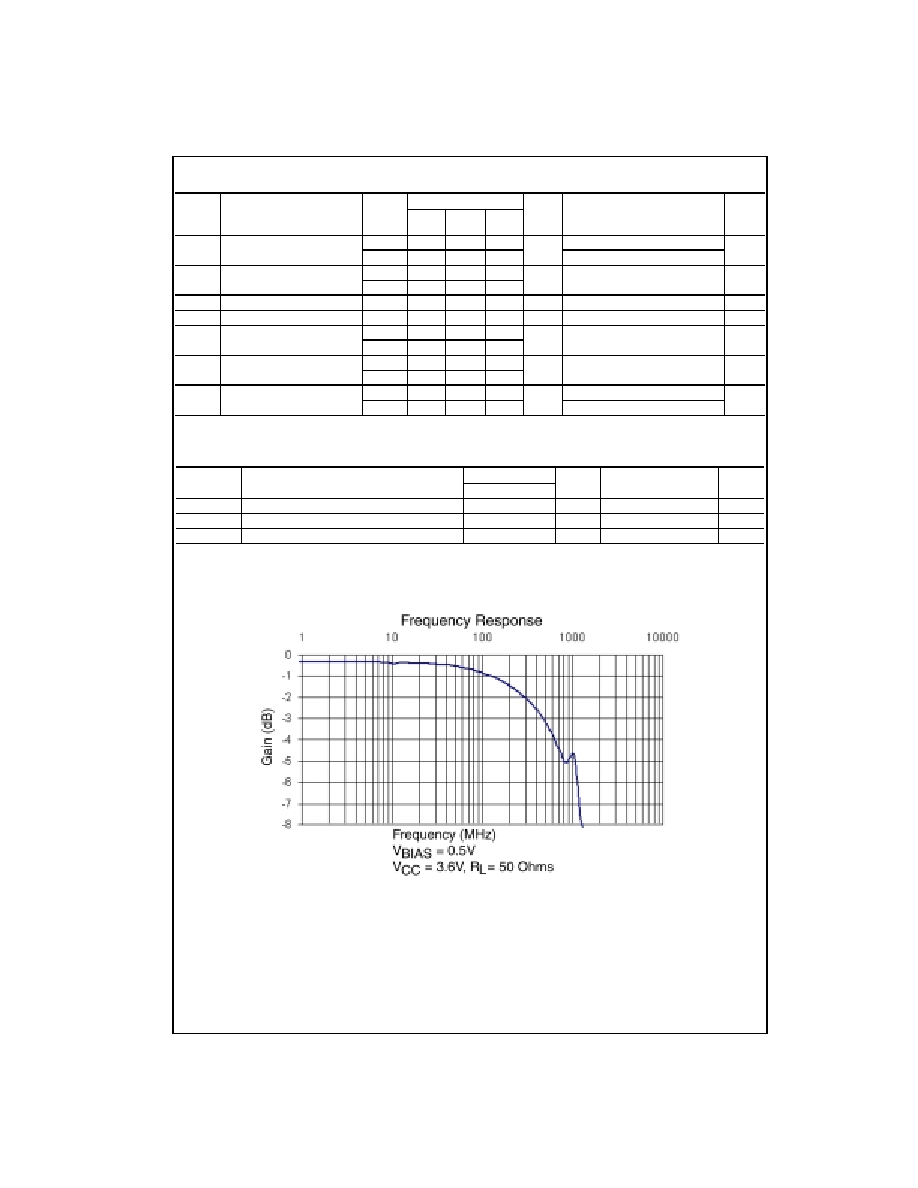
FIGURE 1. Gain vs. Frequency
Symbol
Parameter
V
CC
(V)
T
A
40
q
C to
85
q
C
Units
Conditions
Figure
Number
Min
Typ
(Note 7)
Max
t
ON
Turn ON Time S-to-Bus A
3.0 to 3.6
5.5
ns
V
B
2.0V
Figures
7, 8
2.3 to 2.7
7.0
t
OFF
Turn OFF Time S-to-Bus A
3.0 to 3.6
4.0
ns
V
B
2.0V
Figures
7, 8
2.3 to 2.7
5.0
DG
Differential Gain
3.0 to 3.6
0.2
%
R
L
75
:
, f
3.58MHz
DP
Differential Phase
3.0 to 3.6
0.1
Degree R
L
75
:
, f
3.58MHz
O
IRR
Non-Adjacent OFF-Isolation
3.0 to 3.6
55.0
dB
f
10MHz, R
L
75
:
Figure
10
Adjacent OFF-Isolation
2.3 to 2.7
55.0
X
TALK
Non-Adjacent Channel Crosstalk
3.0 to 3.6
85.0
dB
R
L
75
:
, f
10MHz
Figures
11, 12
Adjacent Channel Crosstalk
2.3 to 2.7
85.0
BW
3dB Bandwidth
3.0 to 3.6
550
MHz
R
L
50
:
Figure 9
3.0 to 3.6
300
R
L
75
:
Symbol
Parameter
T
A
40
q
C to
85
q
C
Units
Conditions
Figure
Typ (Note 8)
Number
C
IN
Control Pin Input Capacitance
3.0
pF
V
CC
0V
C
ON
A/B ON Capacitance
15.0
pF
V
CC
3.0V
0V
Figure 14
C
OFF
Port B OFF Capacitance
4.0
pF
V
CC
3.0V
Figure 13

