©2005 Fairchild Semiconductor Corporation
www.fairchildsemi.com
Rev.1.1.0
FPS
TM
is a trademark of Fairchild Semiconductor Corporation.
Features
∑ Optimized for Quasi-Resonant Converter (QRC)
∑ Advanced Burst-Mode Operation for under 1W Standby
Power Consumption
∑ Pulse-by-Pulse Current Limit
∑ Over Load Protection (OLP) - Auto Restart
∑ Over Voltage Protection (OVP) - Auto Restart
∑ Abnormal Over Current Protection (AOCP) - Latch
∑ Internal Thermal Shutdown (TSD) - Latch
∑ Under Voltage Lock Out (UVLO) with Hysteresis
∑ Low Startup Current (typical : 25uA)
∑ Internal High Voltage SenseFET
∑ Built-in Soft Start (20ms)
∑ Extended Quasi-Resonant Switching
Applications
∑ CTV
∑ Audio Amplifier
Related Application Notes
∑ AN4146 - Design
G
uidelines for Quasi-
R
esonant
C
onverters Using FSCQ-
S
eries Fairchild Power Switch
.
∑ AN4140 - Transformer Design Consideration for Off-
L
ine
F
lyback Converters
U
sing Fairchild Power Switch.
Description
In general, a Quasi-Resonant Converter (QRC) shows lower
EMI and higher power conversion efficiency compared to
conventional hard-switched converter with a fixed switching
frequency. Therefore,
a
QRC is well suited for noise-
sensitive applications, such as color TV and audio. Each
product in the FSCQ-Series contains an integrated Pulse
Width Modulation (PWM) controller and
a
SenseFET, and
is
specifically designed for quasi-resonant off-line Switch
Mode Power Supplies (SMPS) with minimal external
components. The PWM controller includes an integrated fixed
frequency oscillator, under voltage lockout, leading edge
blanking (LEB), optimized gate driver, internal soft start,
temperature-compensated precise current sources for a loop
compensation
,
and self protection circuitry. Compared with
a
discrete MOSFET and PWM controller solution, the FSCQ-
Series can reduce total cost, component count, size
,
and weight,
while simultaneously increasing efficiency, productivity, and
system reliability.
These devices
provide a basic platform
that is well suited for cost-effective designs of quasi-resonant
switching flyback converters.
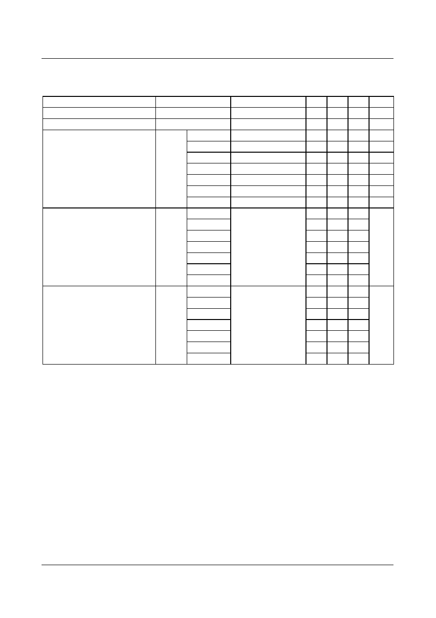
Table 1. Maximum Output Power
Notes:
1. Maximum practical continuous power in an open frame
design at 50
∞
C ambient.
2. 230 VAC or 100/115 VAC with doubler.
3. The junction
t
emperature can limit the
maximum output
power.
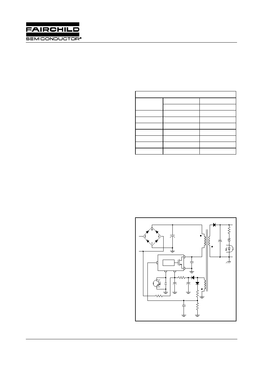
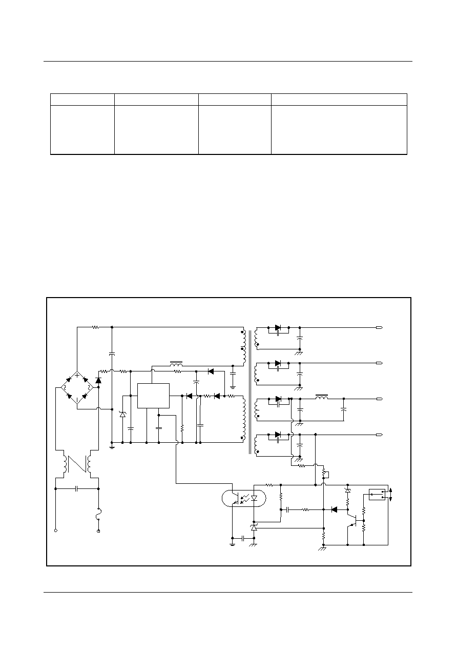
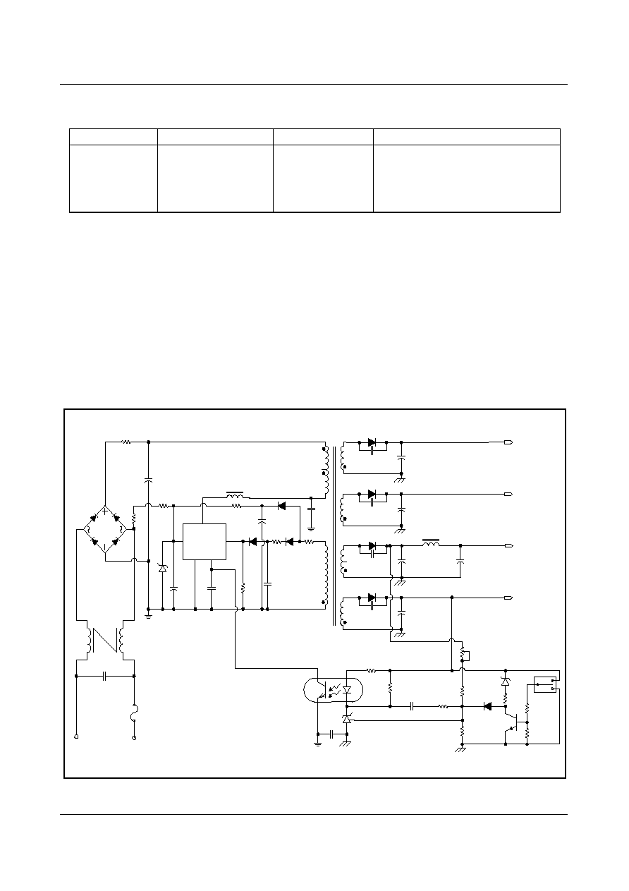
Typical Circuit
Figure 1. Typical Flyback Application
OUTPUT POWER TABLE
(3)
PRODUCT
230VAC
±
15%
(2)
85-265VAC
Open Frame
(1)
Open Frame
(1)
FSCQ0565RT
70W
60 W
FSCQ0765RT
100 W
85 W
FSCQ0965RT
130 W
110 W
FSCQ1265RT
170 W
140 W
FSCQ1465RT
190 W
160 W
FSCQ1565RT
210 W
170 W
FSCQ1565RP
250 W
210 W
Vcc
GND
Drain
Sync
Vo
PWM
V
FB
AC
IN
FSCQ-Series
FSCQ-Series
FSCQ0565RT / FSCQ0765RT / FSCQ0965RT / FSCQ1265RT
FSCQ1465RT / FSCQ1565RT / FSCQ1565RP
Green Mode Fairchild Power Switch (FPS
TM
)
FSCQ-SERIES
2
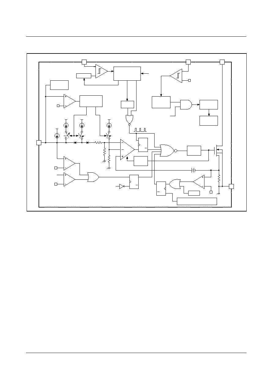
Internal Block Diagram
Figure 2. Functional Block Diagram of FSCQ-Series
9V/15V
3
1
2
4
Auxiliary
Vref
Main Bias
S
Q
Q
R
OSC
Vcc
Vref
I
delay
I
FB
V
SD
TSD
Vovp
Sync
Vocp
S
Q
Q
R
R
2.5R
Vcc good
(Vcc = 9V)
Vcc
Drain
V
FB
GND
AOCP
Gate
Driver
Vcc good
LEB
600ns
PWM
Soft Start
Internal
Bias
Normal
Operation
V
Burst
Vref
I
B
Vref
I
BFB
Burst Mode
Controller
Normal Operation
Burst Switching
5
Sync
Threshold
Quasi-Resonant
(QR) Switching
Controller
+
-
+
-
S
Q
Q
R
Power Off Reset
(Vcc = 6V)
4.6V/2.6V : Normal QR
3.0V/1.8V : Extended QR
fs
FSCQ-SERIES
3
Pin Definitions
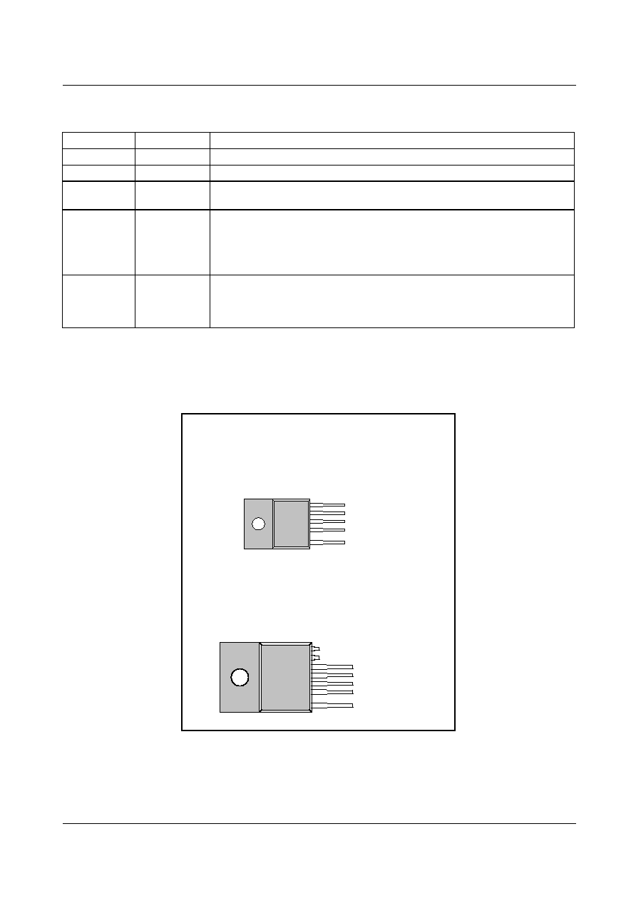
Pin Configuration
Figure 3. Pin Configuration (Top View)
Pin Number
Pin Name
Pin Function Description
1
Drain
High voltage power SenseFET drain connection.
2
GND
This pin is the control ground and the SenseFET source.
3
Vcc
This pin is the positive supply input. This pin provides internal operating
current for both start-up and steady-state operation.
4
Vfb
This pin is internally connected to the inverting input of the PWM comparator.
The collector of an opto-coupler is typically tied to this pin. For stable
operation, a capacitor should be placed between this pin and GND. If the
voltage of this pin reaches 7.5V, the over load protection triggers
,
which
results in the FPS shutting down.
5
Sync
This pin is internally connected to the sync detect comparator for quasi-
resonant switching. In normal quasi-resonant operation, the threshold of the
sync comparator is 4.6V/2.6V. Whereas, the sync threshold is changed to
3.0V/1.8V in an extended quasi-resonant operation.
5.Sync
4.Vfb
3.Vcc
2.GND
1.Drain
TO-220F-5L
5.Sync
4.Vfb
3.Vcc
2.GND
1.Drain
TO-3PF-7L

FSCQ-SERIES
4
Absolute Maximum Ratings
(Ta=25
∞
C, unless otherwise specified)
Parameter
Symbol
Value
Unit
Drain Pin Voltage
V
DS
650
V
Supply Voltage
V
CC
20
V
Analog Input Voltage Range
V
sync
-0.3 to 13V
V
V
FB
-0.3 to V
CC
V
Drain Current Pulsed
(1)
I
DM
FSCQ0565RT
11.2
A
FSCQ0765RT
15.2
FSCQ0965RT
16.4
FSCQ1265RT
21.2
FSCQ1465RT
22
FSCQ1565RT
26.4
FSCQ1565RP
33.2
Continuous Drain Current(Tc=25
∞
C)
(Tc : Case Back Surface Temperature)
I
D
FSCQ0565RT
2.8
A
(rms)
FSCQ0765RT
3.8
FSCQ0965RT
4.1
FSCQ1265RT
5.3
FSCQ1465RT
5.5
FSCQ1565RT
6.6
FSCQ1565RP
8.3
Continuous Drain Current * (T
DL
=25
∞
C)
(T
DL :
Drain Lead Temperature)
I
D
*
FSCQ0565RT
5
A
(rms)
FSCQ0765RT
7
FSCQ0965RT
7.6
FSCQ1265RT
11
FSCQ1465RT
12
FSCQ1565RT
13.3
FSCQ1565RP
15
Continuous Drain Current (T
C
=100
∞
C)
I
D
FSCQ0565RT
1.7
A
(rms)
FSCQ0765RT
2.4
FSCQ0965RT
2.6
FSCQ1265RT
3.4
FSCQ1465RT
3.5
FSCQ1565RT
4.4
FSCQ1565RP
5.5
Single-Pulsed Avalanche Energy
(2)
E
AS
FSCQ0565RT
400
mJ
FSCQ0765RT
570
FSCQ0965RT
630
FSCQ1265RT
950
FSCQ1465RT
1000
FSCQ1565RT
1050
FSCQ1565RP
1050
FSCQ-SERIES
5
Notes:
1. Repetitive rating: Pulse width limited by maximum junction temperature
2. L = 15mH, starting T
j
= 25
∞
C, These parameters, although guaranteed at the design, are not tested in mass production.
Thermal Impedance
(Ta=25
∞
C unless otherwise specified)
Total Power Dissipation
(Tc=25
∞
C with Infinite Heat Sink)
P
D
FSCQ0565RT
38
W
FSCQ0765RT
45
FSCQ0965RT
49
FSCQ1265RT
50
FSCQ1465RT
60
FSCQ1565RT
75
FSCQ1565RP
98
Operating Junction Temperature
T
J
+150
∞
C
Operating Ambient Temperature
T
A
-25 to +85
∞
C
Storage Temperature Range
T
STG
-55 to +150
∞
C
ESD Capability, HBM Model (All pins
except Vfb)
-
2.0
(GND-Vfb=1.7kV)
kV
ESD Capability, Machine Model (All
pins except Vfb)
-
300
(GND-Vfb=170V)
V
Parameter
Symbol
Value
Unit
Junction to Case Thermal Impedance
JC
FSCQ0565RT
3.29
∞
C/W
FSCQ0765RT
2.60
FSCQ0965RT
2.55
FSCQ1265RT
2.50
FSCQ1465RT
2.10
FSCQ1565RT
2.00
FSCQ1565RP
1.28
FSCQ-SERIES
6
Electrical Characteristics (SenseFET Part)
(Ta=25
∞
C unless otherwise specified)
Parameter
Symbol
Condition
Min. Typ. Max.
Unit
Drain-Source Breakdown Voltage
BV
DSS
V
GS
= 0V, I
D
= 250
A 650
-
-
V
Zero Gate Voltage Drain Current
I
DSS
V
DS
= 650V,V
GS
= 0V
-
-
250
A
Drain-Source ON-State
Resistance
R
DS(ON)
FSCQ0565RT
V
GS
= 10V, I
D
= 1A
-
1.76
2.2
FSCQ0765RT
V
GS
= 10V, I
D
= 1A
-
1.4
1.6
FSCQ0965RT
V
GS
= 10V, I
D
= 1A
-
1.0
1.2
FSCQ1265RT
V
GS
= 10V, I
D
= 1A
-
0.75
0.9
FSCQ1465RT
V
GS
= 10V, I
D
= 1A
-
0.7
0.8
FSCQ1565RT
V
GS
= 10V, I
D
= 1A
-
0.53
0.7
FSCQ1565RP
V
GS
= 10V, I
D
= 1A
-
0.53
0.7
Input Capacitance
C
ISS
FSCQ0565RT
V
GS
= 0V, V
DS
= 25V,
f = 1MHz
-
1080
-
pF
FSCQ0765RT
-
1415
-
FSCQ0965RT
-
1750
-
FSCQ1265RT
-
2400
-
FSCQ1465RT
-
2400
-
FSCQ1565RT
-
3050
-
FSCQ1565RP
-
3050
-
Output Capacitance
C
OSS
FSCQ0565RT
V
GS
= 0V, V
DS
= 25V,
f = 1MHz
-
90
-
pF
FSCQ0765RT
-
100
-
FSCQ0965RT
-
130
-
FSCQ1265RT
-
175
-
FSCQ1465RT
-
185
-
FSCQ1565RT
-
220
-
FSCQ1565RP
-
220
-

FSCQ-SERIES
7
Electrical Characteristics
(Continued)
(Ta=25
∞
C unless otherwise specified)
Note:
1. These parameters, although guaranteed, are tested only in EDS (wafer test) process.
2. These parameters, although guaranteed at the design, are not tested in mass production.
Parameter
Symbol
Condition
Min. Typ. Max. Unit
CONTROL SECTION
Switching Frequency
F
OSC
V
FB
= 5V, V
CC
= 18V
18
20
22
kHz
Switching Frequency Variation
(1)
F
OSC
-25
∞
C
Ta
85
∞
C
0
±
5
±10
%
Feedback Source Current
I
FB
V
FB
= 0.8V, V
CC
= 18V
0.5
0.65
0.8
mA
Maximum Duty Cycle
D
MAX
V
FB
= 5V, V
CC
= 18V
92
95
98
%
Minimum Duty Cycle
D
MIN
V
FB
= 0V, V
CC
= 18V
-
0
-
%
UVLO Threshold Voltage
V
START
V
FB
=1V
14
15
16
V
V
STOP
V
FB
=1V
8
9
10
V
Soft Start Time
(1)
T
SS
-
18
20
22
ms
BURST MODE SECTION
Burst Mode Enable Feedback Voltage
V
BEN
-
0.25 0.40 0.55
V
Burst Mode Feedback Source Current
I
BFB
V
FB
= 0V
60
100
140
uA
Burst Mode Switching Time
T
BS
V
FB
= 0.9V, Duty =50%
1.2
1.4
1.6
ms
Burst Mode Hold Time
T
BH
V
FB
= 0.9V -> 0V
1.2
1.4
1.6
ms
PROTECTION SECTION
Shutdown Feedback Voltage
V
SD
V
CC
= 18V
7.0
7.5
8.0
V
Shutdown Delay Current
I
DELAY
V
FB
= 5V, V
CC
= 18V
4
5
6
A
Over Voltage Protection
V
OVP
V
FB
= 3V
11
12
13
V
Over Current Latch Voltage
(1)
V
OCL
V
CC
= 18V
0.9
1.0
1.1
V
Thermal Shutdown Temp
(2)
T
SD
-
140
-
-
∞
C

FSCQ-SERIES
8
Electrical Characteristics
(Continued)
(Ta=25
∞
C unless otherwise specified)
Note:
1. This parameter is the current flowing in the control IC.
2. These parameters indicate inductor current.
3. These parameters, although guaranteed, are tested only in EDS (wafer test) process.
Parameter
Symbol
Condition
Min. Typ. Max. Unit
Sync SECTION
Sync Threshold in Normal QR (H)
V
SH1
V
CC
= 18V, V
FB
= 5V
4.2
4.6
5.0
V
Sync Threshold in Normal QR (L)
V
SL1
2.3
2.6
2.9
V
Sync Threshold in Extended QR (H)
V
SH2
2.7
3.0
3.3
V
Sync Threshold in Extended QR (L)
V
SL2
1.6
1.8
2.0
V
Extended QR Enable Frequency
F
SYH
-
90
-
kHz
Extended QR Disable Frequency
F
SYL
-
45
-
kHz
TOTAL DEVICE SECTION
Operating Supply Current
(1)
- In Normal Operation
I
OP
FSCQ0565RT
V
FB
= 5V
-
4
6
mA
FSCQ0765RT
-
4
6
FSCQ0965RT
-
6
8
FSCQ1265RT
-
6
8
FSCQ1465RT
-
7
9
FSCQ1565RT
-
7
9
FSCQ1565RP
-
7
9
- In Burst Mode (Non-switching)
I
OB
V
FB
= GND
-
0.25 0.50
mA
Startup Current
I
START
V
CC
= V
START
-0.1V
-
25
50
uA
Sustain Latch Current
(3)
I
SN
V
CC
= V
STOP
-0.1V
-
50
100
uA
CURRENT SENSE SECTION
Maximum Current Limit
(2)
I
LIM
FSCQ0565RT
V
CC
= 18V, V
FB
= 5V
3.08
3.5
3.92
A
FSCQ0765RT
4.4
5
5.6
FSCQ0965RT
5.28
6.0
6.72
FSCQ1265RT
6.16
7
7.84
FSCQ1465RT
7.04
8.0
8.96
FSCQ1565RT
7.04
8
8.96
FSCQ1565RP
10.12 11.5 12.88
Burst Peak Current
I
BUR(pk)
FSCQ0565RT
V
CC
= 18V, V
FB
= Pulse
0.45 0.65 0.85
A
FSCQ0765RT
0.65
0.9
1.15
FSCQ0965RT
0.6
0.9
1.2
FSCQ1265RT
0.8
1.2
1.6
FSCQ1465RT
0.6
0.9
1.2
FSCQ1565RT
-
1
-
FSCQ1565RP
-
1
-
FSCQ-SERIES
9
Electrical Characteristics
-50
0
50
100
150
0.8
1.0
1.2
Temp[ ]
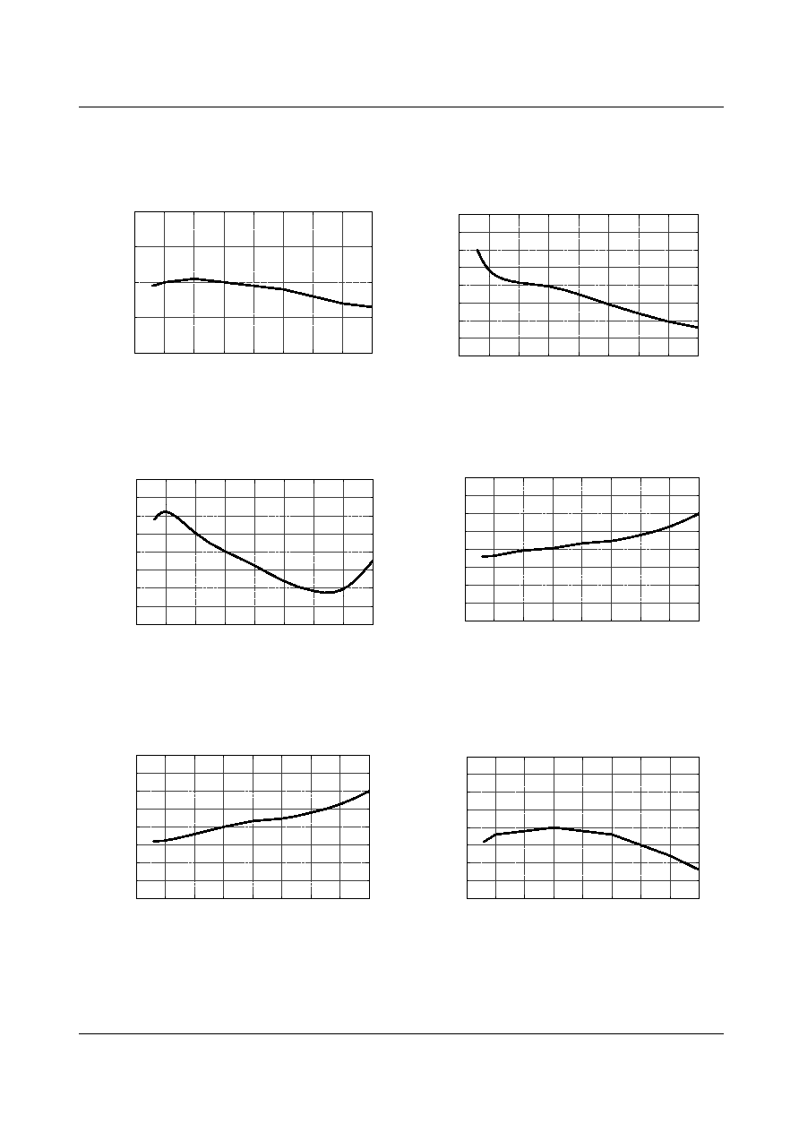
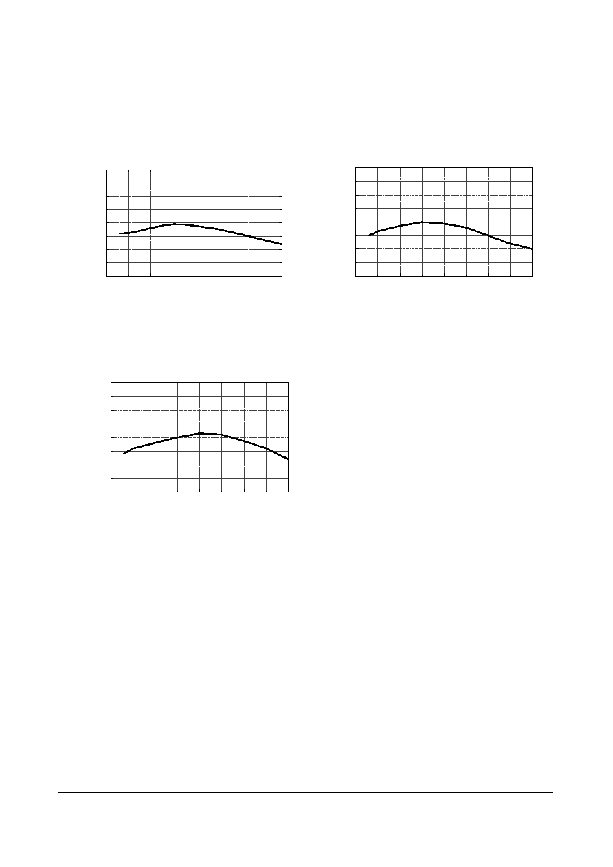
Operating Supply Current
No
r
m
a
l
i
z
ed
to
2
5
-50
0
50
100
150
0.6
0.8
1.0
1.2
1.4
Temp[ ]
Burst-mode Supply Current( Non-Switching)
Normalized to
25
-50
0
50
100
150
0.6
0.8
1.0
1.2
1.4
Temp[ ]
Start-Up Current
No
rma
liz
ed to
2
5
-50
0
50
100
150
0.90
0.95
1.00
1.05
1.10
Temp[ ]
Start Threshold Voltage
Norm
aliz
ed t
o
25
-50
0
50
100
150
0.90
0.95
1.00
1.05
1.10
Temp[ ]
Stop Threshold Voltage
N
o
r
m
alized
to
25
-50
0
50
100
150
0.90
0.95
1.00
1.05
1.10
Initial Frequency
N
o
rma
liz
ed
to 2
5
Temp[ ]
FSCQ-SERIES
10
Electrical Characteristics
-50
0
50
100
150
0.90
0.95
1.00
1.05
1.10
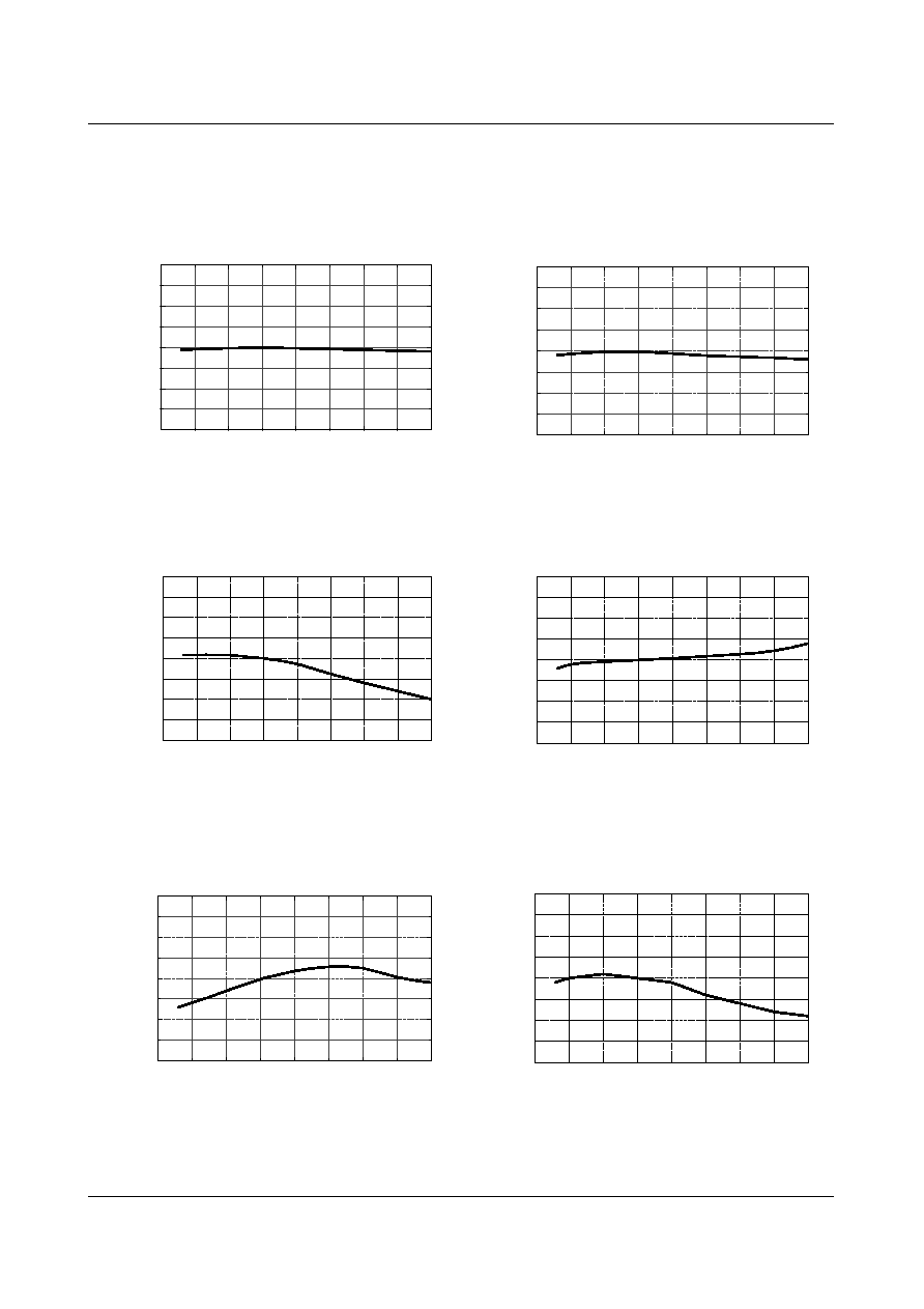
Maximum Duty Cycle
Norm
aliz
ed t
o
25
Temp[ ]
-50
0
50
100
150
0.90
0.95
1.00
1.05
1.10
Temp[ ]
Over Voltage Protection
Normali
z
ed to 25
-50
0
50
100
150
0.8
0.9
1.0
1.1
1.2
Temp[ ]
Shutdown Delay Current
No
rma
l
ized
to
25
-50
0
50
100
150
0.90
0.95
1.00
1.05
1.10
Temp[ ]
Shutdown Feedback Voltage
N
o
rm
ali
z
ed
t
o
25
-50
0
50
100
150
0.8
0.9
1.0
1.1
1.2
Temp[ ]
Feedback Source Current
N
o
rmalized to 25
-50
0
50
100
150
0.8
0.9
1.0
1.1
1.2
Temp[ ]
Burst_mode Feedback Source Current
Normalized
t
o
25
FSCQ-SERIES
11
Electrical Characteristics
-50
0
50
100
150
0.6
0.8
1.0
1.2
1.4
Temp[ ]
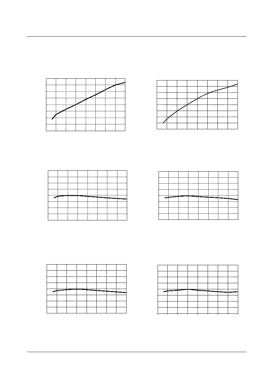
Burst_Mode Enable Feedback Voltage
N
o
rm
aliz
ed
t
o
25
-50
0
50
100
150
0.6
0.8
1.0
1.2
1.4
N
o
rm
alized
to 25
Temp[
]
Feedback Offset Voltage
-50
0
50
100
150
0.90
0.95
1.00
1.05
1.10
Temp[ ]
Sync. Threshold in Normal QR(H)
No
r
m
ali
z
ed to 2
5
-50
0
50
100
150
0.90
0.95
1.00
1.05
1.10
Temp[ ]
Sync. Threshold in Normal QR(L)
Nor
m
aliz
ed
to 25
-50
0
50
100
150
0.90
0.95
1.00
1.05
1.10
Temp[ ]
Sync. Threshold in Extended QR(H)
Normalized to
25
-50
0
50
100
150
0.90
0.95
1.00
1.05
1.10
Temp[ ]
Sync. Threshold in Extended QR(L)
Normalized to
25
FSCQ-SERIES
12
Electrical Characteristics
-50
0
50
100
150
0.90
0.95
1.00
1.05
1.10
Extended QR Enable Freqency
Norma
lize
d
t
o
25
Temp[]
-50
0
50
100
150
0.90
0.95
1.00
1.05
1.10
Normalize
d
to
25
T em p [ ]
P u lse-b y-p ulse C u rren t L im it
-50
0
50
100
150
0.9 0
0.9 5
1.0 0
1.0 5
1.1 0
Normalize
d
to 25
T em p [ ]
E xten d ed Q R D isab le F req u en cy
FSCQ-SERIES
13
Functional Description
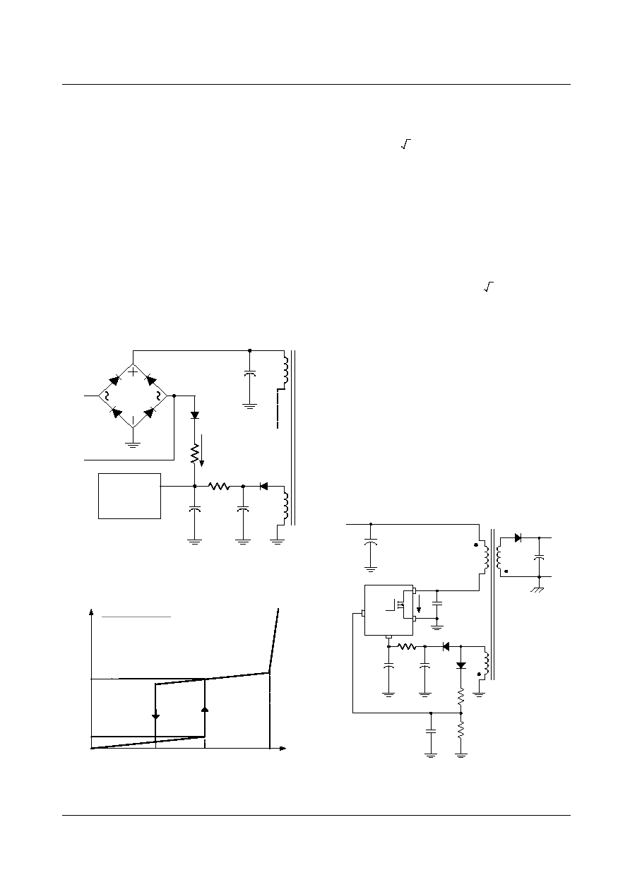
1.
Startup: Figure 4 shows the typical startup circuit and
the
transformer auxiliary winding for
the
FSCQ-Series.
Before
the
FSCQ-Series begins switching, it consumes only
startup current (typically 25uA)
.
T
he current supplied from
the AC line charges the external capacitor (C
a1
) that is
connected to the Vcc pin. When Vcc reaches the start voltage
of 15V (V
START
),
the
FSCQ-Series begins switching, and its
current consumption increases to I
OP
. Then, the FSCQ-
Series continues its normal switching operation and the
power required for the FSCQ-Series is supplied from the
transformer auxiliary winding, unless Vcc drops below the
stop voltage of 9V (V
STOP
). To guarantee the stable operation
of the control IC, Vcc has under voltage lockout (UVLO)
with 6V hysteresis. Figure 5 shows the relationship between
the
operating supply current of
the FSCQ-Series and the
supply voltage (Vcc).
Figure 4. Startup circuit
Figure 5. Relationship Between Operating Supply Current
and Vcc Voltage
The minimum average of the current supplied from the AC is
given by
where V
ac
min
is the minimum input voltage, V
start
is the
FSCQ-Series start voltage (15V)
,
and R
str
is the startup
resistor. The startup resistor should be chosen so that I
sup
avg
is larger than the maximum startup current (50uA).
Once the resistor value is determined, the maximum loss in
the startup resistor is obtained as
where V
ac
max
is the maximum input voltage. The startup
resistor should have properly-rated dissipation wattage.
2. Synchronization: The FSCQ-Series employs a quasi-
resonant switching technique to minimize the switching noise
and loss. In this technique, a capacitor (Cr) is added between
the MOSFET drain and
the
source as shown in Figure 6. The
basic waveforms of the quasi-resonant converter are shown in
Figure 7. The external capacitor lowers the rising slope of the
drain voltage to reduce the EMI caused when the MOSFET
turns off.
To
minimize the MOSFET's switching loss, the
MOSFET should be turned on when the drain voltage reaches
its minimum value as shown in Figure 7.
Figure 6. Synchronization Circuit
FSCQ-Series
1N4007
Rstr
Vcc
C
a1
Da
I
sup
AC line
(V
ac
min
- V
ac
max
)
C
DC
C
a2
Icc
Vcc
Vstop=9V
I
START
I
OP
Vstart=15V
Vz
Power Up
Power Down
I
OP
Value
FSCQ0565RT : 4mA (Typ.)
FSCQ0765RT : 4mA (Typ.)
FSCQ0965RT : 6mA (Typ.)
FSCQ1265RT : 6mA (Typ.)
FSCQ1465RT : 7mA (Typ.)
FSCQ1565RT : 7mA (Typ.)
FSCQ1565RP : 7mA (Typ.)
I
sup
avg
2 V
ac
min
------------------------------
V
start
2
--------------
≠
1
R
str
----------
=
Loss
1
R
str
----------
V
ac
max
(
)
2
V
start
2
+
2
---------------------------------------------------
2 2 V
start
V
ac
max
------------------------------------------------------
≠
=
V
cc
C
a1
D
a
C
DC
C
a2
GND
Cr
Drain
Ids
R
cc
R
SY1
R
SY2
Sync
+
V
DC
-
Lm
Vo
C
SY
+
V
ds
-
V
co
D
SY
Np
Ns
Na

FSCQ-SERIES
14
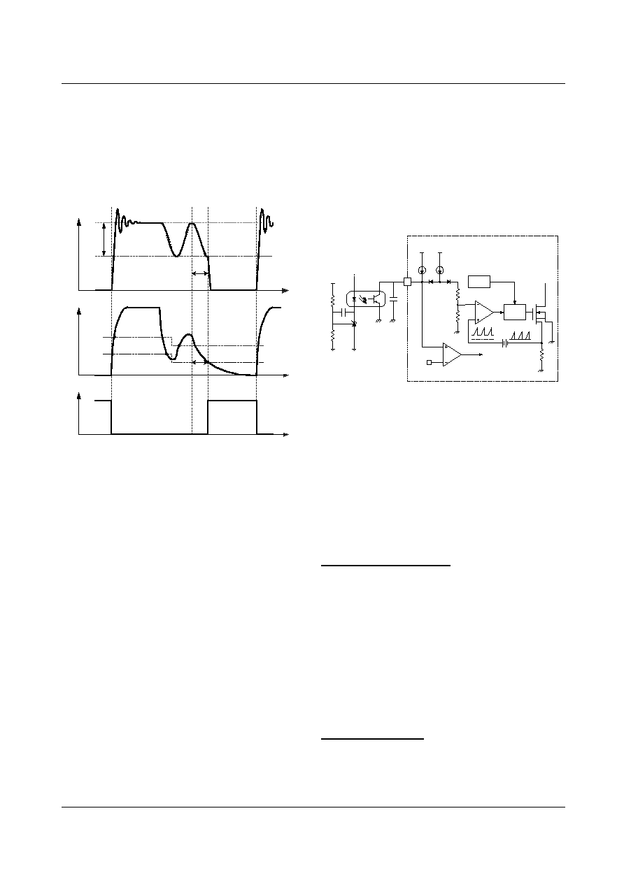
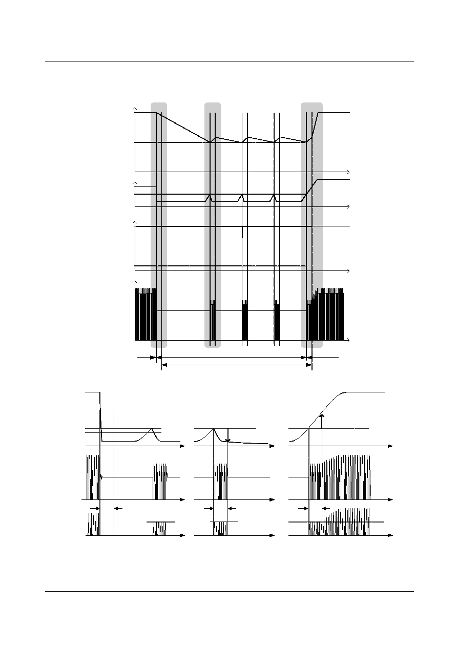
Figure 7. Quasi-resonant Operation Waveforms
The minimum drain voltage is indirectly detected by
monitoring the Vcc winding voltage as shown in Figure 6
and 8.
Choose
voltage dividers, R
SY1
and R
SY2,
so that the
peak voltage of the sync signal (V
sypk
) is lower than the
OVP voltage (12V)
to
avoid triggering OVP in normal
operation. It is typical to set V
sypk
to be lower than OVP
voltage by 3-4 V.
T
o detect the optimum time to turn on
MOSFET, the sync capacitor (C
SY
) should be determined so
that T
R
is the same with T
Q as shown in Figure 8
. The T
R
and
T
Q
are given as, respectively
where L
m
is the primary side inductance of the transformer,
and
N
s
and N
a
are the number of turns for the output
winding and Vcc winding, respectively
,
V
Fo
and V
Fa
are the
diode forward voltage drops of the output winding and Vcc
winding, respectively, and C
eo
is the sum of the output
capacitance of the MOSFET and the external capacitor, Cr.
Figure 8. Normal Quasi-Resonant Operation Waveforms
Figure 9. Extended Quasi-Resonant Operation
In general, the QRC has a limitation in a wide load range
application, since the switching frequency increases as the
output load decreases, resulting in a severe switching loss in
the light load condition.
To
overcome
this limitation, the
FSCQ-Series employs an extended quasi-resonant switching
operation. Figure 9 shows the mode change between normal
and extended quasi-resonant operations. In the normal quasi-
resonant operation, the FSCQ-Series enters into the extended
quasi-resonant operation when the switching frequency
exceeds 90kHz as the load
reduces
. To reduce the switching
frequency, the MOSFET is turned on when the drain voltage
reaches the second minimum level, as shown in Figure 10.
V
DC
V
RO
V
RO
I
pk
I
ds
V
d
s
V
gs
MOSFET
Off
MOSFET
On
T
R
R
SY2
C
SY
V
co
2.6
---------
R
SY2
R
SY1
R
SY2
+
-----------------------------------
ln
=
T
Q
L
m
C
eo
=
V
co
N
a
V
o
V
FO
+
(
)
N
s
-----------------------------------------
V
Fa
≠
=
Vs ync
Vds
MOS FET Gate
2V
R O
Vrh (4.6V)
Vrf (2.6V)
ON
T
Q
T
R
ON
V
sypk
Output power
Switching
frequency
Normal QR operation
Extended QR operation
90kHz
45kHz
FSCQ-SERIES
15
Once the FSCQ-Series enters into
the
extended quasi-
resonant operation, the first sync signal is ignored. After the
first sync signal is applied, the sync threshold levels are
changed from 4.6V and 2.6V to 3V and 1.8V, respectively,
and the MOSFET turn-on time is synchronized to the second
sync signal. The FSCQ-Series returns to its normal quasi-
resonant operation when the switching frequency reaches
45kHz as the load increases.
Figure 10. Extended Quasi-Resonant Operation Wave-
forms
3. Feedback Control:
The
FSCQ-Series employs current
mode control, as shown in Figure 11. An opto-coupler (such
as
Fairchild's
H11A817A) and shunt regulator (such as
Fairchild's
KA431) are typically used to implement the
feedback network. Comparing the feedback voltage with the
voltage across the Rsense resistor plus an offset voltage
makes it possible to control the switching duty cycle. When
the reference pin voltage of the KA431 exceeds the internal
reference voltage of 2.5V, the H11A817A LED current
increases, pulling down the feedback voltage and reducing
the duty cycle. This event typically happens when the input
voltage is increased or the output load is decreased.
3.1 Pulse-by-
P
ulse Current Limit: Because current mode
control is employed, the peak current through the
SenseFET
is limited by the inverting input of the PWM
comparator (Vfb*) as shown in Figure 11. The feedback
current (I
FB
) and internal resistors are designed so that the
maximum cathode voltage of diode D
2
is about 2.8V, which
occurs when all I
FB
flows through the internal resistors.
Since D
1
is blocked when the feedback voltage (Vfb)
exceeds 2.8V, the maximum voltage of the cathode of D2 is
clamped at this voltage, thus clamping Vfb*. Therefore, the
peak value of the current through the SenseFET is limited.
3.2 Leading Edge Blanking (LEB) : At the instant the
internal Sense FET is turned on, there is usually a high
current spike through the Sense FET, caused by the external
resonant capacitor across the MOSFET and secondary-side
rectifier reverse recovery. Excessive voltage across the
R
sense
resistor can lead to incorrect feedback operation in
the current mode PWM control. To counter this effect, the
FSCQ-Series employs a leading edge blanking (LEB)
circuit. This circuit inhibits the PWM comparator for a short
time (T
LEB
) after the Sense FET is turned on.
Figure 11. Pulse Width Modulation (PWM) Circuit
4. Protection Circuits: The FSCQ-Series has several self-
protective functions such as over load protection (OLP),
abnormal over current protection (AOCP), over voltage
protection (OVP)
,
and thermal shutdown (TSD). OLP and
OVP are auto-restart mode protection
s
, while TSD and
AOCP are latch mode protection
s
. Because these protection
circuits are fully integrated into the IC without external
components, the reliability can be improved without
increasing cost.
-Auto-restart mode protection: Once the fault condition is
detected, switching is terminated and the SenseFET remains
off. This causes Vcc to fall. When Vcc falls to the under
voltage lockout (UVLO) stop voltage of 9V, the protection is
reset and
the
FSCQ-Series consumes only startup current
(25uA). Then, the Vcc capacitor is charged up, since the
current supplied through the startup resistor is larger than the
current that
the
FPS consumes. When Vcc reaches the start
voltage of 15V, the FSCQ-Series resumes its normal
operation. If the fault condition is not removed, the
SenseFET remains off and Vcc drops to stop voltage again.
In this manner, the auto-restart can alternately enable and
disable the switching of the power SenseFET until the fault
condition is eliminated (see Figure 12).
-Latch mode protection: Once this protection is triggered,
switching is terminated and the Sense FET remains off until
the AC power line is un-plugged. Then, Vcc continues
charging and discharging between 9V and 15V. The latch is
reset only when Vcc is discharged to 6V by un-plugging the
Vsync
Vds
MOSFET Gate
2V
RO
4.6V
2.6V
3V
1.8V
ON
ON
4
OSC
Vcc
Vref
I
delay
I
FB
V
SD
R
2.5R
Gate
driver
OLP
D1
D2
+
V
fb
*
-
Vfb
KA431
C
B
Vo
H11A817A
R
sense
SenseFET

FSCQ-SERIES
16
AC power line.
Figure 12. Auto Restart Mode Protection
4.1 Over Load Protection (OLP): Overload is defined as
the load current exceeding its normal level due to an
unexpected abnormal event. In this situation, the protection
circuit should trigger to protect the SMPS. However, even
when the SMPS is in the normal operation, the over load
protection circuit can be triggered during the load transition.
To avoid this undesired operation, the over load protection
circuit is designed to trigger after a specified time to
determine whether it is a transient situation or an overload
situation. Because of the pulse-by-pulse current limit
capability, the maximum peak current through the SenseFET
is limited, and therefore the maximum input power is
restricted with a given input voltage. If the output consumes
more than this maximum power, the output voltage (Vo)
decreases below the set voltage. This reduces the current
through the opto-coupler LED, which also reduces the opto-
coupler transistor current, thus increasing the feedback
voltage (Vfb). If Vfb exceeds 2.8V, D1 is blocked
,
and the
5uA current source starts to charge C
B
slowly up to Vcc. In
this condition, Vfb continues increasing until it reaches 7.5V,
then
the switching operation is terminated as shown in
Figure 13. The delay time for shutdown is the time required
to charge C
B
from 2.8V to 7.5V with 5uA. In general, a 20 ~
50 ms delay time is typical for most applications.
OLP
is
implemented in auto restart mode.
Figure 13. Over Load Protection
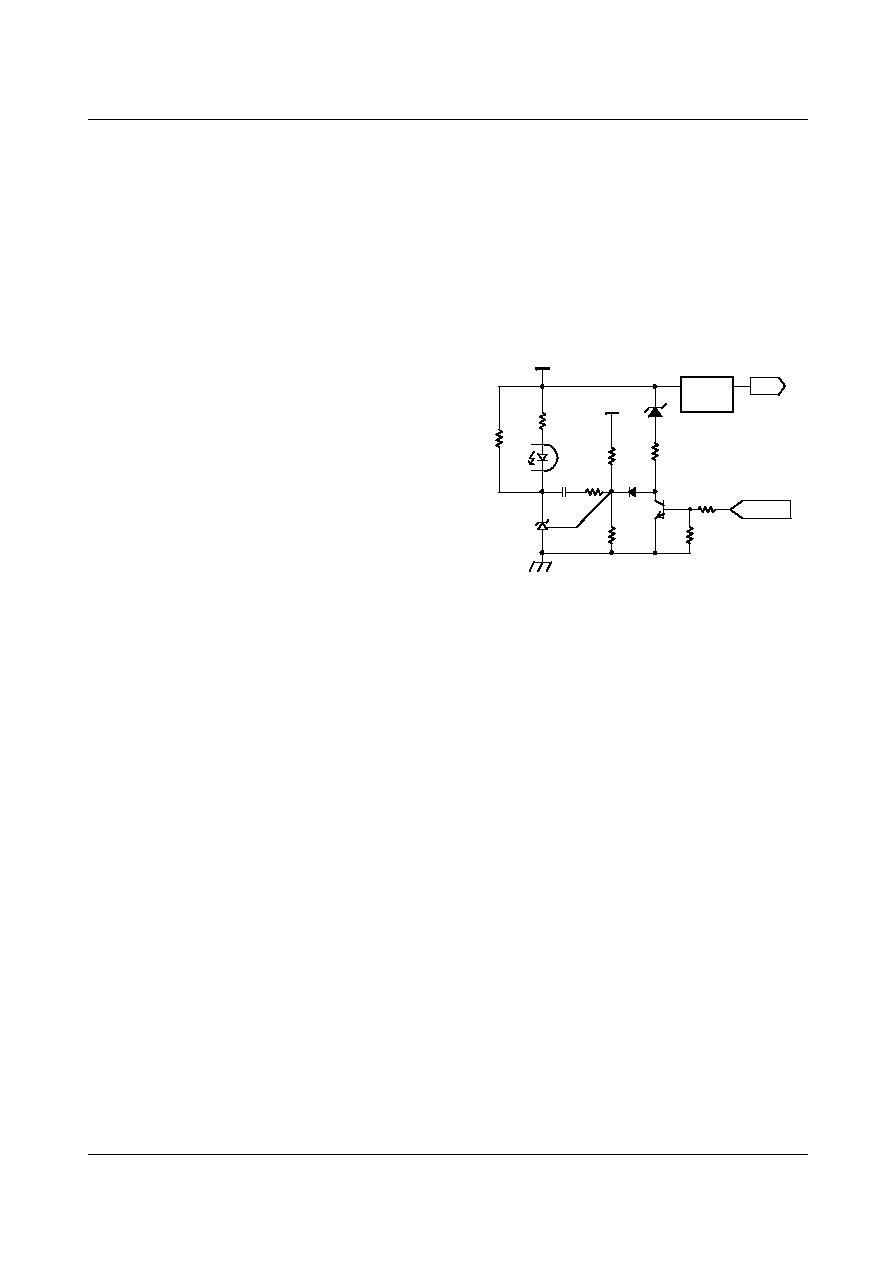
4.2 Abnormal Over Current Protection (AOCP): When
the secondary rectifier diodes or the transformer pins are
shorted, a steep current with extremely high di/dt can flow
through the SenseFET during the LEB time. Even though the
FSCQ-Series has OLP (Over Load Protection), it is not
enough to protect the FSCQ-Series in that abnormal case,
since severe current stress will be imposed on the SenseFET
until
the
OLP triggers. The FSCQ-Series has an internal
AOCP (Abnormal Over Current Protection) circuit as shown
in Figure 14. When the gate turn-on signal is applied to the
power SenseFET, the AOCP block is enabled and monitors
the current through the sensing resistor. The voltage across
the resistor is then compared with a preset AOCP level. If
the sensing resistor voltage is greater than the AOCP level,
the set signal is applied to the latch, resulting in the
shutdown of SMPS. This protection is implemented in the
latch mode.
Figure 14. AOCP Block
4.3 Over Voltage Protection (OVP) : If the secondary side
feedback circuit malfunctions or a solder defect causes an
open in the feedback path, the current through the opto-
coupler transistor becomes almost zero. Then, Vfb climbs up
in a similar manner to the over load situation, forcing the
Fault
situation
9V
15V
Vcc
Vds
I
CC
I
OP
t
Fault
occurs
Fault
removed
Normal
operation
Normal
operation
Power
on
I
START
V
FB
t
2.8V
7.5V
Over load protection
T
12
= C
B
*(7.5-2.8)/I
delay
T
1
T
2
2
S
Q
Q
R
OSC
R
2.5R
GND
Gate
Driver
LEB
PWM
+
-
Vaocp
AOCP
R
sense
FSCQ-SERIES
17
preset maximum current to be supplied to the SMPS until the
over load protection triggers. Because more energy than
required is provided to the output, the output voltage may
exceed the rated voltage before the over load protection
triggers, resulting in the breakdown of the devices in the
secondary side. In order to prevent this situation, an over
voltage protection (OVP) circuit is employed. In general, the
peak voltage of the sync signal is proportional to the output
voltage and the FSCQ-Series uses a sync signal instead of
directly monitoring the output voltage. If the sync signal
exceeds 12V, an OVP is triggered resulting in a shutdown of
SMPS. In order to avoid undesired triggering of OVP during
normal operation, the peak voltage of the sync signal should
be designed to be below 12V. This protection is implemented
in the auto restart mode.
4.4 Thermal Shutdown (TSD) : The SenseFET and the
control IC are built in one package. This makes it easy for
the control IC to detect abnormal over temperature of the
SenseFET. When the temperature exceeds approximately
150
∞C, the thermal shutdown triggers. This protection is
implemented in the latch mode.
5. Soft Start : The FSCQ-Series has an internal soft-start
circuit that increases PWM comparator's inverting input
voltage together with the SenseFET current slowly after it
starts up. The typical soft start time is 20msec. The pulse
width to the power switching device is progressively
increased to establish the correct working conditions for
transformers, inductors, and capacitors. Increasing the pulse
width to the power switching device also helps prevent
transformer saturation and reduces the stress on the
secondary diode during startup. For a fast build up of the
output voltage, an offset is introduced in the soft-start
reference current.
6. Burst Operation : In order to minimize the power
consumption in the standby mode, the FSCQ-Series employs
burst operation. Once FSCQ-Series enters into the burst
mode, FSCQ-Series allows all output voltages and effective
switching frequency to be reduced. Figure 15 shows the
typical feedback circuit for C-TV applications. In normal
operation, the picture on signal is applied and the transistor
Q
1
is turned on, which de-couples R
3
, D
z
and D1 from the
feedback network. Therefore, only V
o1
is regulated by the
feedback circuit in normal operation and determined by R
1
and R
2
as
In the standby mode, the picture ON signal is disabled and
the transistor Q
1
is turned off, which couples R
3
, Dz, and D
1
to the reference pin of KA431. Then, Vo2 is determined by
the zener diode breakdown voltage. Assuming that the
forward voltage drop of D
1
is 0.7V, V
o2
in standby mode is
approximately given by
Figure 15. Typical Feedback Circuit to Drop Output Volt-
age in Standby Mode
Figure 17 shows the burst mode operation waveforms. When
the picture ON signal is disabled, Q
1
is turned off and R
3
and Dz are connected to the reference pin of KA431 through
D
1
. Before V
o2
drops to V
o2
stby
, the voltage on the reference
pin of KA431 is higher than 2.5V, which increases the
current through the opto LED. This pulls down the feedback
voltage (V
FB
) of FSCQ-Series and forces FSCQ-Series to
stop switching. If the switching is disabled longer than
1.4ms, FSCQ-Series enters into burst operation and the
operating current is reduced from I
OP
to 0.25mA (I
OB
). Since
there is no switching, V
o2
decreases until it reaches V
o2
stby
.
As V
o2
reaches V
o2
stby
, the current through the opto LED
decreases allowing the feedback voltage to rise. When the
feedback voltage reaches 0.4V, FSCQ-Series resumes
switching with a predetermined peak drain current of 0.9A.
After burst switching for 1.4ms, FSCQ-Series stops
switching and checks the feedback voltage. If the feedback
voltage is below 0.4V, FSCQ-Series stops switching until the
feedback voltage increases to 0.4V. If the feedback voltage is
above 0.4V, FSCQ-Series goes back to the normal operation.
The output voltage drop circuit can be implemented
alternatively as shown in Figure 16. In the circuit of Figure
16, the FSCQ-Series goes into burst mode, when picture off
signal is applied to Q1. Then, Vo2 is determined by the zener
diode breakdown voltage. Assuming that the forward
V
o1
norm
2.5
R
1
R
2
+
R
2
---------------------
=
V
o2
stby
V
Z
0.7
2.5
+
+
=
Picture ON
Micom
Linear
Regulator
V
O2
V
O1
(B+)
KA431
R
2
R
1
R
3
R
bias
R
D
R
F
C
F
D
1
Q1
A
C
R
Dz

FSCQ-SERIES
18
voltage drop of opto LED is 1V, the approcimate value of
V
o2
in standby mode is given by
Figure 16. Feedback Circuit to Drop Output Voltage in
Standby Mode
V
o2
stby
V
Z
1
+
=
Picture OFF
Micom
Linear
Regulator
V
O2
V
O1
(B+)
KA431
R
2
R
1
R
bias
R
D
R
F
C
F
A
C
R
Dz
Q
1
FSCQ-SERIES
19
Figure 17. Burst Operation Waveforms
V
o2
norm
V
FB
Iop
Vds
0.4V
V
o2
stby
I
OP
Picture On
Picture Off
I
OB
Picture On
Burst Mode
(a)
(c)
(b)
0.4V
0.9A
1.4ms
(b) Burst Operation
(c) Mode Change to Normal Operation
V
FB
V
ds
I
ds
0.3V
0.4V
1.4ms
(a) Mode Change to Burst Operation
0.4V
0.9A
1.4ms
FSCQ-SERIES
20
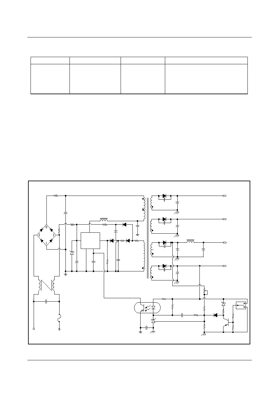
FSCQ0565RT Typical Application Circuit
Features
∑ High
E
fficiency (>83% at 90Vac
I
nput)
∑ Wider
L
oad
R
ange through the
E
xtended
Q
uasi-
R
esonant
O
peration
∑ Low Standby Mode Power Consumption (<1W)
∑ Low Component Count
∑ Enhanced System Reliability Through Various Protection Functions
∑ Internal Soft-Start (20ms)
Key Design Notes
∑ 24V output is designed to drop to around 8V in standby mode
1. Schematic
Application
Output Power
Input Voltage
Output Voltage (Max Current)
C-TV
59W
Universal Input
(90-270Vac)
12V (0.5A)
18V (0.3A)
125V (0.3A)
24V (0.4A)
C103
10uF
50V
1
3
4
10
T1
EER3540
12V, 0.5A
C204
1000uF
35V
D205
EGP20D
11
LF101
C101
330nF
275VAC
FUSE
250V
2.0A
C102
220uF
400V
RT101
5D-9
BD101
D101
1N4937
R103
5.1
0.25W
6
7
R104
1.5k
0.25W
2
4
5
1
3
GND
Drain
SYNC
FB
Vcc
D103
1N4148
IC101
FSCQ0565RT
C106
47nF
50V
R105
470
0.25W
C105
3.9nF
50V
ZD101
18V
1W
C107
680pF
1kV
BEAD101
D102
1N4937
C210
470pF
1kV
18V, 0.3A
D204
EGP20D
C205
1000uF
35V
13
C209
470pF
1kV
12
125V, 0.3A
D202
EGP20J
C201
100uF
160V
14
C207
470pF
1kV
L201
BEAD
16
C202
47uF
160V
24V, 0.4A
D203
EGP20D
C203
1000uF
35V
17
C208
470pF
1kV
18
OPTO101
FOD817A
R201
1k
0.25W
C206
22nF
50V
C301
2.2nF
Q201
KA431
R203
39k
0.25W
R202
1k
0.25W
R205
220k
0.25W
R204
4.7k
0.25W
VR201
30k
D201
Q202
KSC945
R206
5.1k
0.25W
R207
5.1k
0.25W
SW201
15
R102
150k
0.25W
R101
100k
0.25W
R106
1.5k
1W
C104
10uF
50V
ZD202
5.1V
0.5W
R208
1k
0.25W
Normal
Standby
D104
UF4007
ZD201
FSCQ-SERIES
21
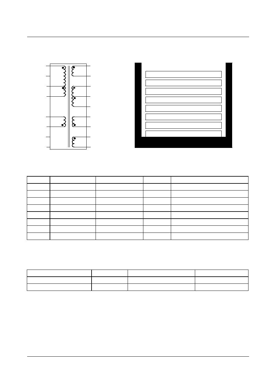
2. Transformer Schematic Diagram
3.Winding Specification
4.Electrical Characteristics
5. Core & Bobbin
Core : EER3540
Bobbin : EER3540
Ae : 107 mm
2
No
Pin (s
f)
Wire
Turns
Winding Method
N
p1
1 - 3
0.5
◊
1
32
Center Winding
N
125V/2
16 - 15
0.5
◊
1
32
Center Winding
N
24V
18 - 17
0.4
◊
2
13
Center Winding
N
12V
12 - 13
0.5
◊
2
7
Center Winding
N
p2
3 - 4
0.5
◊
1
32
Center Winding
N
125V/2
15 - 14
0.5
◊
1
32
Center Winding
N
18V
11 - 10
0.4
◊
2
10
Center Winding
N
a
7 - 6
0.3
◊
1
20
Center Winding
Pin
Specification
Remarks
Inductance
1 - 3
740uH ± 5%
1kHz, 1V
Leakage Inductance
1 - 3
10uH Max
2
nd
all short
EER3540
N
24V
N
a
7
13
14
15
16
17
18
N
125V
/2
N
12V
N
18V
N
p1
N
p2
1
2
3
4
5
6
8
9
10
11
12
N
125V
/2
N
125V
/2
N
p2
N
12V
N
125V
/2
N
24V
N
p1
N
18V
N
a

FSCQ-SERIES
22
6.Demo Circuit Part List
Part
Value
Note
Part
Value
Note
Fuse
C210
470pF / 1kV
Ceramic Capacitor
FUSE
250V / 2A
C301
2.2nF / 1kV
AC Ceramic Capacitor
NTC
Inductor
RT101
5D-9
BEAD101
BEAD
Resistor
BEAD201
5uH
3A
R101
100k
0.25 W
Diode
R102
150k
0.25 W
D101
1N4937
1A, 600V
R103
5.1
0.25 W
D102
1N4937
1A, 600V
R104
1.5k
0.25 W
D103
1N4148
0.15A, 50V
R105
470
0.25 W
D104
Short
R106
1.5k
1 W
D105
Open
R107
Open
ZD101
1N4746
18V, 1W
R201
1k
0.25 W
ZD102
Open
R202
1k
0.25 W
ZD201
1N5231
5.1V, 0.5W
R203
39k
0.25 W
D201
1N4148
0.15A, 50V
R204
4.7k
0.25 W, 1%
D202
EGP20J
2A, 600V
R205
220k
0.25 W, 1%
D203
EGP20D
2A, 200V
R206
5.1k
0.25 W
D204
EGP20D
2A, 200V
R207
5.1k
0.25 W
D205
EGP20D
2A, 200V
R208
1k
0.25 W
VR201
30k
Bridge Diode
Capacitor
BD101
GSIB660
6A, 600V
C101
330n/275VAC
Box Capacitor
Line Filter
C102
220uF / 400V
Electrolytic
LF101
14mH
C103
10uF / 50V
Electrolytic
Transformer
C104
10uF / 50V
Electrolytic
T101
EER3540
C105
3.9nF / 50V
Film Capacitor
Switch
C106
47nF / 50V
Film Capacitor
SW201
ON/OFF
For MCU Signal
C107
680pF / 1kV
Film Capacitor
IC
C108
Open
IC101
FSCQ0565RT
TO-220F-5L
C201
100uF / 160V
Electrolytic
OPT101
FOD817A
C202
47uF / 160V
Electrolytic
Q201
KA431LZ
TO-92
C203
1000uF / 35V
Electrolytic
Q202
KSC945
C204
1000uF / 35V
Electrolytic
C205
1000uF / 35V
Electrolytic
C206
22nF / 50V
Film Capacitor
C207
470pF / 1kV
Ceramic Capacitor
C208
470pF / 1kV
Ceramic Capacitor
C209
470pF / 1kV
Ceramic Capacitor

FSCQ-SERIES
23
FSCQ0765RT Typical Application Circuit
Features
∑ High
E
fficiency (>83% at 90Vac
I
nput)
∑ Wider
L
oad
R
ange through the
E
xtended
Q
uasi-
R
esonant
O
peration
∑ Low Standby Mode Power Consumption (<1W)
∑ Low Component Count
∑ Enhanced System Reliability Through Various Protection Functions
∑ Internal Soft-Start (20ms)
Key Design Notes
∑ 24V output is designed to drop to around 8V in standby mode
1. Schematic
Application
Output Power
Input Voltage
Output Voltage (Max Current)
C-TV
83W
Universal input
(90-270Vac)
12V (1A)
18V (0.5A)
125V (0.4A)
24V (0.5A)
C103
10uF
50V
1
3
4
10
T1
EER3540
12V, 1.0A
C204
1000uF
35V
D205
EGP20D
11
LF101
C101
330nF
275VAC
FUSE
250V
2.0A
C102
220uF
400V
RT101
5D-9
BD101
D101
1N4937
R103
5.1
0.25W
6
7
R104
1.5k
0.25W
2
4
5
1
3
GND
Drain
SYNC
FB
Vcc
D103
1N4148
IC101
FSCQ0765RT
C106
47nF
50V
R105
470
0.25W
C105
3.9nF
50V
ZD101
18V
1W
C107
1nF
1kV
BEAD101
D102
1N4937
C210
470pF
1kV
18V, 0.5A
D204
EGP20D
C205
1000uF
35V
13
C209
470pF
1kV
12
125V, 0.4A
D202
EGP20J
C201
100uF
160V
14
C207
470pF
1kV
L201
BEAD
16
C202
47uF
160V
24V, 0.5A
D203
EGP20D
C203
1000uF
35V
17
C208
470pF
1kV
18
OPTO101
FOD817A
R201
1k
0.25W
C206
22nF
50V
C301
2.2nF
Q201
KA431
R203
39k
0.25W
R202
1k
0.25W
R205
220k
0.25W
R204
4.7k
0.25W
VR201
30k
D201
Q202
KSC945
R206
5.1k
0.25W
R207
5.1k
0.25W
SW201
15
R102
150k
0.25W
R101
100k
0.25W
R106
1.5k
1W
C104
10uF
50V
ZD202
5.1V
0.5W
R208
1k
0.25W
Normal
Standby
D104
UF4007
ZD201

FSCQ-SERIES
24
2. Transformer Schematic Diagram
3.Winding Specification
4.Electrical Characteristics
5. Core & Bobbin
Core : EER3540
Bobbin : EER3540
Ae : 107 mm
2
No
Pin (s
f)
Wire
Turns
Winding Method
N
p1
1 - 3
0.5
◊
1
32
Center Winding
N
125V/2
16 - 15
0.5
◊
1
32
Center Winding
N
24V
18 - 17
0.4
◊
2
13
Center Winding
N
12V
12 - 13
0.5
◊
2
7
Center Winding
N
p2
3 - 4
0.5
◊
1
32
Center Winding
N
125V/2
15 - 14
0.5
◊
1
32
Center Winding
N
18V
11 - 10
0.4
◊
2
10
Center Winding
N
a
7 - 6
0.3
◊
1
20
Center Winding
Pin
Specification
Remarks
Inductance
1 - 3
515uH ± 5%
1kHz, 1V
Leakage Inductance
1 - 3
10uH Max
2
nd
all short
EER3540
N
24V
N
a
7
13
14
15
16
17
18
N
125V
/2
N
12V
N
18V
N
p1
N
p2
1
2
3
4
5
6
8
9
10
11
12
N
125V
/2
N
125V
/2
N
p2
N
12V
N
125V
/2
N
24V
N
p1
N
18V
N
a

FSCQ-SERIES
25
6.Demo Circuit Part List
Part
Value
Note
Part
Value
Note
Fuse
C210
470pF / 1kV
Ceramic Capacitor
FUSE
250V / 2A
C301
2.2nF / 1kV
AC Ceramic Capacitor
NTC
Inductor
RT101
5D-9
BEAD101
BEAD
Resistor
BEAD201
5uH
3A
R101
100k
0.25 W
Diode
R102
150k
0.25 W
D101
1N4937
1A, 600V
R103
5.1
0.25 W
D102
1N4937
1A, 600V
R104
1.5k
0.25 W
D103
1N4148
0.15A, 50V
R105
470
0.25 W
D104
Short
R106
1.5k
1 W
D105
Open
R107
Open
ZD101
1N4746
18V, 1W
R201
1k
0.25 W
ZD102
Open
R202
1k
0.25 W
ZD201
1N5231
5.1V, 0.5W
R203
39k
0.25 W
D201
1N4148
0.15A, 50V
R204
4.7k
0.25 W, 1%
D202
EGP20J
2A, 600V
R205
220k
0.25 W, 1%
D203
EGP20D
2A, 200V
R206
5.1k
0.25 W
D204
EGP20D
2A, 200V
R207
5.1k
0.25 W
D205
EGP20D
2A, 200V
R208
1k
0.25 W
VR201
30k
Bridge Diode
Capacitor
BD101
GSIB660
6A, 600V
C101
330n/275VAC
Box Capacitor
Line Filter
C102
220uF / 400V
Electrolytic
LF101
14mH
C103
10uF / 50V
Electrolytic
Transformer
C104
10uF / 50V
Electrolytic
T101
EER3540
C105
3.9nF / 50V
Film Capacitor
Switch
C106
47nF / 50V
Film Capacitor
SW201
ON/OFF
For MCU Signal
C107
1nF / 1kV
Film Capacitor
IC
C108
Open
IC101
FSCQ0765RT
TO-220F-5L
C201
100uF / 160V
Electrolytic
OPT101
FOD817A
C202
47uF / 160V
Electrolytic
Q201
KA431LZ
TO-92
C203
1000uF / 35V
Electrolytic
Q202
KSC945
C204
1000uF / 35V
Electrolytic
C205
1000uF / 35V
Electrolytic
C206
22nF / 50V
Film Capacitor
C207
470pF / 1kV
Ceramic Capacitor
C208
470pF / 1kV
Ceramic Capacitor
C209
470pF / 1kV
Ceramic Capacitor

FSCQ-SERIES
26
FSCQ0965RT Typical Application Circuit
Features
∑ High
E
fficiency (>83% at 90Vac
I
nput)
∑ Wider
L
oad
R
ange through the
E
xtended
Q
uasi-
R
esonant
O
peration
∑ Low Standby Mode Power Consumption (<1W)
∑ Low Component Count
∑ Enhanced System Reliability Through Various Protection Functions
∑ Internal Soft-Start (20ms)
Key Design Notes
∑ 24V output is designed to drop to around 8V in standby mode
1. Schematic
Application
Output Power
Input Voltage
Output Voltage (Max Current)
C-TV
102W
Universal input
(90-270Vac)
12V (0.5A)
18V (0.5A)
125V (0.5A)
24V (1.0A)
C103
10uF
50V
1
3
4
10
T1
EER3540
12V, 0.5A
C204
1000uF
35V
D205
EGP20D
11
LF101
C101
330nF
275VAC
FUSE
250V
3.0A
C102
220uF
400V
RT101
5D-9
BD101
D101
1N4937
R103
5.1
0.25W
6
7
R104
1.5k
0.25W
2
4
5
1
3
GND
Drain
SYNC
FB
Vcc
D103
1N4148
IC101
FSCQ0965RT
C106
47nF
50V
R105
470
0.25W
C105
3.9nF
50V
ZD101
18V
1W
C107
1nF
1kV
BEAD101
D102
1N4937
C210
470pF
1kV
18V, 0.5A
D204
EGP20D
C205
1000uF
35V
13
C209
470pF
1kV
12
125V, 0.5A
D202
EGP30J
C201
100uF
160V
14
C207
470pF
1kV
L201
BEAD
16
C202
47uF
160V
24V, 1.0A
D203
EGP30D
C203
1000uF
35V
17
C208
470pF
1kV
18
OPTO101
FOD817A
R201
1k
0.25W
C206
22nF
50V
C301
2.2nF
Q201
KA431
R203
39k
0.25W
R202
1k
0.25W
R205
220k
0.25W
R204
4.7k
0.25W
VR201
30k
D201
Q202
KSC945
R206
5.1k
0.25W
R207
5.1k
0.25W
SW201
15
R102
150k
0.25W
R101
100k
0.25W
R106
1.5k
1W
C104
10uF
50V
ZD202
5.1V
0.5W
R208
1k
0.25W
Normal
Standby
D104
UF4007
ZD201

FSCQ-SERIES
27
2. Transformer Schematic Diagram
3.Winding Specification
4.Electrical Characteristics
5. Core & Bobbin
Core : EER3540
Bobbin : EER3540
Ae : 107 mm
2
No
Pin (s
f)
Wire
Turns
Winding Method
N
p1
1 - 3
0.6
◊
1
32
Center Winding
N
125V/2
16 - 15
0.6
◊
1
32
Center Winding
N
24V
18 - 17
0.4
◊
2
13
Center Winding
N
12V
12 - 13
0.5
◊
2
7
Center Winding
N
p2
3 - 4
0.6
◊
1
32
Center Winding
N
125V/2
15 - 14
0.6
◊
1
32
Center Winding
N
18V
11 - 10
0.4
◊
2
10
Center Winding
N
a
7 - 6
0.3
◊
1
20
Center Winding
Pin
Specification
Remarks
Inductance
1 - 3
410uH ± 5%
1kHz, 1V
Leakage Inductance
1 - 3
10uH Max
2
nd
all short
EER3540
N
24V
N
a
7
13
14
15
16
17
18
N
125V
/2
N
12V
N
18V
N
p1
N
p2
1
2
3
4
5
6
8
9
10
11
12
N
125V
/2
N
125V
/2
N
p2
N
12V
N
125V
/2
N
24V
N
p1
N
18V
N
a

FSCQ-SERIES
28
6.Demo Circuit Part List
Part
Value
Note
Part
Value
Note
Fuse
C210
470pF / 1kV
Ceramic Capacitor
FUSE
250V / 3A
C301
3.3nF / 1kV
AC Ceramic Capacitor
NTC
Inductor
RT101
5D-9
BEAD101
BEAD
Resistor
BEAD201
5uH
3A
R101
100k
0.25 W
Diode
R102
150k
0.25 W
D101
1N4937
1A, 600V
R103
5.1
0.25 W
D102
1N4937
1A, 600V
R104
1.5k
0.25 W
D103
1N4148
0.15A, 50V
R105
470
0.25 W
D104
Short
R106
1.5k
1 W
D105
Open
R107
Open
ZD101
1N4746
18V, 1W
R201
1k
0.25 W
ZD102
Open
R202
1k
0.25 W
ZD201
1N5231
5.1V, 0.5W
R203
39k
0.25 W
D201
1N4148
0.15A, 50V
R204
4.7k
0.25 W, 1%
D202
EGP30J
3A, 600V
R205
220k
0.25 W, 1%
D203
EGP30D
3A, 200V
R206
5.1k
0.25 W
D204
EGP20D
2A, 200V
R207
5.1k
0.25 W
D205
EGP20D
2A, 200V
R208
1k
0.25 W
VR201
30k
Bridge Diode
Capacitor
BD101
GSIB660
6A, 600V
C101
330n/275VAC
Box Capacitor
Line Filter
C102
220uF / 400V
Electrolytic
LF101
14mH
C103
10uF / 50V
Electrolytic
Transformer
C104
10uF / 50V
Electrolytic
T101
EER3540
C105
3.9nF / 50V
Film Capacitor
Switch
C106
47nF / 50V
Film Capacitor
SW201
ON/OFF
For MCU Signal
C107
1nF / 1kV
Film Capacitor
IC
C108
Open
IC101
FSCQ0965RT
TO-220F-5L
C201
100uF / 160V
Electrolytic
OPT101
FOD817A
C202
47uF / 160V
Electrolytic
Q201
KA431LZ
TO-92
C203
1000uF / 35V
Electrolytic
Q202
KSC945
C204
1000uF / 35V
Electrolytic
C205
1000uF / 35V
Electrolytic
C206
22nF / 50V
Film Capacitor
C207
470pF / 1kV
Ceramic Capacitor
C208
470pF / 1kV
Ceramic Capacitor
C209
470pF / 1kV
Ceramic Capacitor
FSCQ-SERIES
29
FSCQ1265RT Typical Application Circuit
Features
∑ High
E
fficiency (>83% at 90Vac
I
nput)
∑ Wider
L
oad
R
ange through the
E
xtended
Q
uasi-
R
esonant
O
peration
∑ Low Standby Mode Power Consumption (<1W)
∑ Low Component Count
∑ Enhanced System Reliability Through Various Protection Functions
∑ Internal Soft-Start (20ms)
Key Design Notes
∑ 24V output is designed to drop to around 8V in standby mode
1. Schematic
Application
Output Power
Input Voltage
Output Voltage (Max Current)
C-TV
132W
Universal input
(90-270Vac)
8.5V (0.5A)
15V (0.5A)
140V (0.6A)
24V (1.5A)
C103
10uF
50V
1
3
4
10
T1
EER4042
15V, 0.5A
C204
1000uF
35V
D205
EGP20D
11
LF101
C101
330nF
275VAC
FUSE
250V
5.0A
C102
330uF
400V
RT101
5D-11
BD101
D103
1N4937
R103
5.1
0.25W
6
7
R104
1.5k
0.25W
2
4
5
1
3
GND
Drain
SYNC
FB
Vcc
D106
1N4148
IC101
FSCQ1265RT
C106
47nF
50V
R105
470
0.25W
C105
3.3nF
50V
ZD102
18V
1W
C107
1nF
1kV
BEAD101
D105
1N4937
C210
470pF
1kV
8.5V, 0.5A
D204
EGP20D
C205
1000uF
35V
13
C209
470pF
1kV
12
140V, 0.6A
D202
EGP30J
C201
150uF
160V
14
C207
470pF
1kV
L202
BEAD
16
C202
68uF
160V
24V, 1.5A
D203
EGP30D
C203
1000uF
35V
17
C208
470pF
1kV
18
OPTO101
FOD817A
R201
1k
0.25W
C206
150nF
50V
C301
3.3nF
Q201
KA431
LZ
R203
39k
0.25W
R202
1k
0.25W
R205
240k
0.25W
R204
4.7k
0.25W
VR201
30k
D201
1N4148
Q202
KSC945
R206
10k
0.25W
R207
5.1k
0.25W
SW201
15
R102
150k
0.25W
R101
100k
0.25W
R106
1k
1W
C104
10uF
50V
ZD201
5.1V
0.5W
R208
1k
0.25W

FSCQ-SERIES
30
2. Transformer Schematic Diagram
3.Winding Specification
4.Electrical Characteristics
5. Core & Bobbin
Core : EER4042
Bobbin : EER4042(18Pin)
Ae : 153 mm
2
No
Pin (s
f)
Wire
Turns
Winding Method
N
24
18 - 17
0.65
◊
2
8
Space Winding
N
p1
1 - 3
0.1
◊
10
◊
2
20
Center Winding
N
140V/2
16 - 15
0.1
◊
10
◊
2
23
Center Winding
N
p2
3 - 4
0.1
◊
10
◊
2
20
Center Winding
N
140V/2
15 - 14
0.1
◊
10
◊
2
22
Center Winding
N
8.5V
12 - 13
0.6
◊
1
3
Space Winding
N
15V
11 - 10
0.6
◊ 1
6
Space Winding
N
a
7 - 6
0.3
◊
1
13
Space Winding
Pin
Specification
Remarks
Inductance
1 - 4
315uH ± 5%
1kHz, 1V
Leakage Inductance
1 - 4
10uH Max
2
nd
all short
EER4042
N
24V
N
a
7
13
14
15
16
17
18
N
140V
/2
N
8.5V
N
15V
N
p1
N
p2
1
2
3
4
5
6
8
9
10
11
12
N
140V
/2
N
8.5V
N
140V/2
N
P2
N
P1
N
140V/2
N
24V
N
15V
N
a

FSCQ-SERIES
31
6.Demo Circuit Part List
Part
Value
Note
Part
Value
Note
Fuse
C210
470pF / 1kV
Ceramic Capacitor
FUSE
250V / 5A
C301
3.3nF / 1kV
AC Ceramic Capacitor
NTC
Inductor
RT101
5D-11
BEAD101
BEAD
Resistor
BEAD201
5uH
3A
R101
100k
0.25 W
Diode
R102
150k
0.25 W
D101
1N4937
1A, 600V
R103
5.1
0.25 W
D102
1N4937
1A, 600V
R104
1.5k
0.25 W
D103
1N4148
0.15A, 50V
R105
470
0.25 W
D104
Short
R106
1k
1 W
D105
Open
R107
Open
ZD101
1N4746
18V, 1W
R201
1k
0.25 W
ZD102
Open
R202
1k
0.25 W
ZD201
1N5231
5.1V, 0.5W
R203
39k
0.25 W
D201
1N4148
0.15A, 50V
R204
4.7k
0.25 W, 1%
D202
EGP30J
3A, 600V
R205
240k
0.25 W, 1%
D203
EGP30D
3A, 200V
R206
10k
0.25 W
D204
EGP20D
2A, 200V
R207
5.1k
0.25 W
D205
EGP20D
2A, 200V
R208
1k
0.25 W
VR201
30k
Bridge Diode
Capacitor
BD101
GSIB660
6A, 600V
C101
330n/275Vac
Box Capacitor
Line Filter
C102
330uF / 400V
Electrolytic
LF101
14mH
C103
10uF / 50V
Electrolytic
Transformer
C104
10uF / 50V
Electrolytic
T101
EER4042
C105
3.3nF / 50V
Film Capacitor
Switch
C106
47nF / 50V
Film Capacitor
SW201
ON/OFF
For MCU Signal
C107
1nF / 1kV
Film Capacitor
IC
C108
Open
IC101
FSCQ1265RT
TO-220F-5L
C201
150uF / 160V
Electrolytic
OPT101
FOD817A
C202
68uF / 160V
Electrolytic
Q201
KA431LZ
TO-92
C203
1000uF / 35V
Electrolytic
Q202
KSC945
C204
1000uF / 35V
Electrolytic
C205
1000uF / 35V
Electrolytic
C206
150nF / 50V
Film Capacitor
C207
470pF / 1kV
Ceramic Capacitor
C208
470pF / 1kV
Ceramic Capacitor
C209
470pF / 1kV
Ceramic Capacitor
FSCQ-SERIES
32
FSCQ1465RT Typical Application Circuit
Features
∑ High
E
fficiency (>83% at 90Vac
I
nput)
∑ Wider
L
oad
R
ange through the
E
xtended
Q
uasi-
R
esonant
O
peration
∑ Low Standby Mode Power Consumption (<1W)
∑ Low Component Count
∑ Enhanced System Reliability Through Various Protection Functions
∑ Internal Soft-Start (20ms)
Key Design Notes
∑ 24V output is designed to drop to around 8V in standby mode
1. Schematic
Application
Output Power
Input Voltage
Output Voltage (Max Current)
C-TV
146W
Universal input
(90-270Vac)
8.5V (0.5A)
15V (0.5A)
140V (0.7A)
24V (1.5A)
C103
10uF
50V
1
3
4
10
T1
EER4245
15V, 0.5A
C204
1000uF
35V
D205
EGP20D
11
LF101
C101
330nF
275VAC
FUSE
250V
5.0A
C102
330uF
400V
RT101
6D-22
BD101
D103
1N4937
R103
5.1
0.25W
6
7
R104
1.5k
0.25W
2
4
5
1
3
GND
Drain
SYNC
FB
Vcc
D106
1N4148
IC101
FSCQ1465RT
C106
47nF
50V
R105
470
0.25W
C105
2.7nF
50V
ZD102
18V
1W
C107
1nF
1kV
BEAD101
D105
1N4937
C210
470pF
1kV
8.5V, 0.5A
D204
EGP20D
C205
1000uF
35V
13
C209
470pF
1kV
12
140V, 0.7A
D202
EGP30J
C201
150uF
160V
14
C207
470pF
1kV
L202
BEAD
16
C202
68uF
160V
24V, 1.5A
D203
EGP30D
C203
1000uF
35V
17
C208
470pF
1kV
18
OPTO101
FOD817A
R201
1k
0.25W
C206
150nF
50V
C301
3.3nF
Q201
KA431
LZ
R203
39k
0.25W
R202
1k
0.25W
R205
240k
0.25W
R204
4.7k
0.25W
VR201
30k
D201
1N4148
Q202
KSC945
R206
10k
0.25W
R207
5.1k
0.25W
SW201
15
R102
150k
0.25W
R101
100k
0.25W
R106
1k
1W
C104
10uF
50V
ZD201
5.1V
0.5W
R208
1k
0.25W

FSCQ-SERIES
33
2. Transformer Schematic Diagram
3.Winding Specification
4.Electrical Characteristics
5. Core & Bobbin
Core : EER4245
Bobbin : EER4245(18Pin)
Ae : 201.8 mm
2
No
Pin (s
f)
Wire
Turns
Winding Method
N
24
18 - 17
0.65
◊
2
5
Space Winding
N
p1
1 - 3
0.08
◊
20
◊
2
13
Center Winding
N
140V/2
16 - 15
0.08
◊
20
◊
2
15
Center Winding
N
p2
3 - 4
0.08
◊
20
◊
2
13
Center Winding
N
140V/2
15 - 14
0.08
◊
20
◊
2
14
Center Winding
N
8.5V
12 - 13
0.6
◊
1
2
Space Winding
N
15V
11 - 10
0.6
◊ 1
3
Space Winding
N
a
7 - 6
0.3
◊
1
8
Space Winding
Pin
Specification
Remarks
Inductance
1 - 4
260uH ± 5%
1kHz, 1V
Leakage Inductance
1 - 4
10uH Max
2
nd
all short
EER4245
N
24V
N
a
7
13
14
15
16
17
18
N
140V
/2
N
8.5V
N
15V
N
p1
N
p2
1
2
3
4
5
6
8
9
10
11
12
N
140V
/2
N
8.5V
N
140V/2
N
P2
N
P1
N
140V/2
N
24V
N
15V
N
a

FSCQ-SERIES
34
6.Demo Circuit Part List
Part
Value
Note
Part
Value
Note
Fuse
C210
470pF / 1kV
Ceramic Capacitor
FUSE
250V / 5A
C301
3.3nF / 1kV
AC Ceramic Capacitor
NTC
Inductor
RT101
6D-22
BEAD101
BEAD
Resistor
BEAD201
5uH
3A
R101
100k
0.25 W
Diode
R102
150k
0.25 W
D101
1N4937
1A, 600V
R103
5.1
0.25 W
D102
1N4937
1A, 600V
R104
1.5k
0.25 W
D103
1N4148
0.15A, 50V
R105
470
0.25 W
D104
Short
R106
1k
1 W
D105
Open
R107
Open
ZD101
1N4746
18V, 1W
R201
1k
0.25 W
ZD102
Open
R202
1k
0.25 W
ZD201
1N5231
5.1V, 0.5W
R203
39k
0.25 W
D201
1N4148
0.15A, 50V
R204
4.7k
0.25 W, 1%
D202
EGP30J
3A, 600V
R205
240k
0.25 W, 1%
D203
EGP30D
3A, 200V
R206
10k
0.25 W
D204
EGP20D
2A, 200V
R207
5.1k
0.25 W
D205
EGP20D
2A, 200V
R208
1k
0.25 W
VR201
30k
Bridge Diode
Capacitor
BD101
GSIB660
6A, 600V
C101
330n/275VAC
Box Capacitor
Line Filter
C102
330uF / 400V
Electrolytic
LF101
14mH
C103
10uF / 50V
Electrolytic
Transformer
C104
10uF / 50V
Electrolytic
T101
EER3540
C105
2.7nF / 50V
Film Capacitor
Switch
C106
47nF / 50V
Film Capacitor
SW201
ON/OFF
For MCU Signal
C107
1nF / 1kV
Film Capacitor
IC
C108
Open
IC101
FSCQ1465RT
TO-220F-5L
C201
150uF / 160V
Electrolytic
OPT101
FOD817A
C202
68uF / 160V
Electrolytic
Q201
KA431LZ
TO-92
C203
1000uF / 35V
Electrolytic
Q202
KSC945
C204
1000uF / 35V
Electrolytic
C205
1000uF / 35V
Electrolytic
C206
150nF / 50V
Film Capacitor
C207
470pF / 1kV
Ceramic Capacitor
C208
470pF / 1kV
Ceramic Capacitor
C209
470pF / 1kV
Ceramic Capacitor

FSCQ-SERIES
35
FSCQ1565RT Typical Application Circuit
Features
∑ High
E
fficiency (>83% at 90Vac
I
nput)
∑ Wider
L
oad
R
ange through the
E
xtended
Q
uasi-
R
esonant
O
peration
∑ Low Standby Mode Power Consumption (<1W)
∑ Low Component Count
∑ Enhanced System Reliability Through Various Protection Functions
∑ Internal Soft-Start (20ms)
Key Design Notes
∑ 24V output is designed to drop to around 8V in standby mode
1. Schematic
Application
Output Power
Input Voltage
Output Voltage (Max Current)
C-TV
160W
Universal input
(90-270Vac)
8.5V (0.5A)
15V (0.5A)
140V (0.8A)
24V (1.5A)
C103
10uF
50V
1
3
4
10
T1
EER4245
15V, 0.5A
C204
1000uF
35V
D205
EGP20D
11
LF101
C101
330nF
275VAC
FUSE
250V
5.0A
C102
470uF
400V
RT101
6D-22
BD101
D103
1N4937
R103
5.1
0.25W
6
7
R104
1.5k
0.25W
2
4
5
1
3
GND
Drain
SYNC
FB
Vcc
D106
1N4148
IC101
FSCQ1565RT
C106
47nF
50V
R105
470
0.25W
C105
2.7nF
50V
ZD102
18V
1W
C107
1nF
1kV
BEAD101
D105
1N4937
C210
470pF
1kV
8.5V, 0.5A
D204
EGP20D
C205
1000uF
35V
13
C209
470pF
1kV
12
140V, 0.8A
D202
EGP30J
C201
220uF
160V
14
C207
470pF
1kV
L202
BEAD
16
C202
68uF
160V
24V, 1.5A
D203
EGP30D
C203
1000uF
35V
17
C208
470pF
1kV
18
OPTO101
FOD817A
R201
1k
0.25W
C206
150nF
50V
C301
3.3nF
Q201
KA431
LZ
R203
39k
0.25W
R202
1k
0.25W
R205
240k
0.25W
R204
4.7k
0.25W
VR201
30k
D201
1N4148
Q202
KSC945
R206
10k
0.25W
R207
5.1k
0.25W
SW201
15
R102
150k
0.25W
R101
100k
0.25W
R106
1k
1W
C104
10uF
50V
ZD201
5.1V
0.5W
R208
1k
0.25W
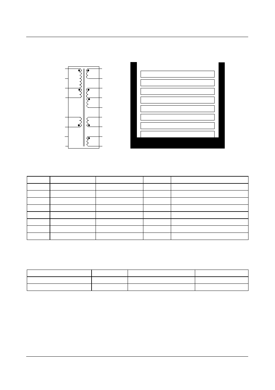
FSCQ-SERIES
36
2. Transformer Schematic Diagram
3.Winding Specification
4.Electrical Characteristics
5. Core & Bobbin
Core : EER4245
Bobbin : EER4245(18Pin)
Ae : 201.8 mm
2
No
Pin (s
f)
Wire
Turns
Winding Method
N
24
18 - 17
0.65
◊
2
5
Space Winding
N
p1
1 - 3
0.08
◊
20
◊
2
13
Center Winding
N
140V/2
16 - 15
0.08
◊
20
◊
2
15
Center Winding
N
p2
3 - 4
0.08
◊
20
◊
2
13
Center Winding
N
140V/2
15 - 14
0.08
◊
20
◊
2
14
Center Winding
N
8.5V
12 - 13
0.6
◊
1
2
Space Winding
N
15V
11 - 10
0.6
◊ 1
3
Space Winding
N
a
7 - 6
0.3
◊
1
8
Space Winding
Pin
Specification
Remarks
Inductance
1 - 4
220uH ± 5%
1kHz, 1V
Leakage Inductance
1 - 4
10uH Max
2
nd
all short
EER4245
N
24V
N
a
7
13
14
15
16
17
18
N
140V
/2
N
8.5V
N
15V
N
p1
N
p2
1
2
3
4
5
6
8
9
10
11
12
N
140V
/2
N
8.5V
N
140V/2
N
P2
N
P1
N
140V/2
N
24V
N
15V
N
a

FSCQ-SERIES
37
6.Demo Circuit Part List
Part
Value
Note
Part
Value
Note
Fuse
C210
470pF / 1kV
Ceramic Capacitor
FUSE
250V / 5A
C301
3.3nF / 1kV
AC Ceramic Capacitor
NTC
Inductor
RT101
6D-22
BEAD101
BEAD
Resistor
BEAD201
5uH
3A
R101
100k
0.25 W
Diode
R102
150k
0.25 W
D101
1N4937
1A, 600V
R103
5.1
0.25 W
D102
1N4937
1A, 600V
R104
1.5k
0.25 W
D103
1N4148
0.15A, 50V
R105
470
0.25 W
D104
Short
R106
1k
1 W
D105
Open
R107
Open
ZD101
1N4746
18V, 1W
R201
1k
0.25 W
ZD102
Open
R202
1k
0.25 W
ZD201
1N5231
5.1V, 0.5W
R203
39k
0.25 W
D201
1N4148
0.15A, 50V
R204
4.7k
0.25 W, 1%
D202
EGP30J
3A, 600V
R205
240k
0.25 W, 1%
D203
EGP30D
3A, 200V
R206
10k
0.25 W
D204
EGP20D
2A, 200V
R207
5.1k
0.25 W
D205
EGP20D
2A, 200V
R208
1k
0.25 W
VR201
30k
Bridge Diode
Capacitor
BD101
GSIB660
6A, 600V
C101
330n/275Vac
Box Capacitor
Line Filter
C102
470uF / 400V
Electrolytic
LF101
14mH
C103
10uF / 50V
Electrolytic
Transformer
C104
10uF / 50V
Electrolytic
T101
EER4245
C105
2.7nF / 50V
Film Capacitor
Switch
C106
47nF / 50V
Film Capacitor
SW201
ON/OFF
For MCU Signal
C107
1nF / 1kV
Film Capacitor
IC
C108
Open
IC101
FSCQ1565RT
TO-220F-5L
C201
220uF / 160V
Electrolytic
OPT101
FOD817A
C202
68uF / 160V
Electrolytic
Q201
KA431LZ
TO-92
C203
1000uF / 35V
Electrolytic
Q202
KSC945
C204
1000uF / 35V
Electrolytic
C205
1000uF / 35V
Electrolytic
C206
150nF / 50V
Film Capacitor
C207
470pF / 1kV
Ceramic Capacitor
C208
470pF / 1kV
Ceramic Capacitor
C209
470pF / 1kV
Ceramic Capacitor

FSCQ-SERIES
38
FSCQ1565RP Typical Application Circuit
Features
∑ High
E
fficiency (>83% at 90Vac
I
nput)
∑ Wider
L
oad
R
ange through the
E
xtended
Q
uasi-
R
esonant
O
peration
∑ Low Standby Mode Power Consumption (<1W)
∑ Low Component Count
∑ Enhanced System Reliability Through Various Protection Functions
∑ Internal Soft-Start (20ms)
Key Design Notes
∑ 24V output is designed to drop to around 8V in standby mode
1. Schematic
Application
Output Power
Input Voltage
Output Voltage (Max Current)
C-TV
198W
Universal input
(90-270Vac)
8.5V (1A)
15V (1A)
140V (0.9A)
24V (2A)
C103
10uF
50V
1
3
4
10
T1
EER4942
15V, 1A
C204
1000uF
35V
D205
EGP20D
11
LF101
C101
330nF
275VAC
FUSE
250V
5.0A
C102
470uF
400V
RT101
6D-22
BD101
D103
1N4937
R103
5.1
0.25W
6
7
R104
1.5k
0.25W
2
4
5
1
3
GND
Drain
SYNC
FB
Vcc
D106
1N4148
IC101
FSCQ1565RP
C106
47nF
50V
R105
470
0.25W
C105
2.7nF
50V
ZD102
18V
1W
C107
1nF
1kV
BEAD101
D105
1N4937
C210
470pF
1kV
8.5V, 1A
D204
EGP20D
C205
1000uF
35V
13
C209
470pF
1kV
12
140V, 0.9A
D202
EGP30J
C201
220uF
160V
14
C207
470pF
1kV
L202
BEAD
16
C202
100uF
160V
24V, 2A
D203
EGP30D
C203
2200uF
35V
17
C208
470pF
1kV
18
OPTO101
FOD817A
R201
1k
0.25W
C206
22nF
50V
C301
3.3nF
Q201
KA431
LZ
R203
39k
0.25W
R202
1k
0.25W
R205
240k
0.25W
R204
4.7k
0.25W
VR201
30k
D201
1N4148
Q202
KSC945
R206
10k
0.25W
R207
5.1k
0.25W
SW201
15
R102
150k
0.25W
R101
100k
0.25W
R106
1k
1W
C104
10uF
50V
ZD201
5.1V
0.5W
R208
1k
0.25W

FSCQ-SERIES
39
2. Transformer Schematic Diagram
3.Winding Specification
4.Electrical Characteristics
5. Core & Bobbin
Core : EER4942
Bobbin : EER4942(18Pin)
Ae : 231 mm
2
No
Pin (s
f)
Wire
Turns
Winding Method
N
24
18 - 17
0.65
◊
2
5
Space Winding
N
p1
1 - 3
0.08
◊
20
◊
2
13
Center Winding
N
140V/2
16 - 15
0.08
◊
20
◊
2
15
Center Winding
N
p2
3 - 4
0.08
◊
20
◊
2
13
Center Winding
N
140V/2
15 - 14
0.08
◊
20
◊
2
14
Center Winding
N
8.5V
12 - 13
0.6
◊
1
2
Space Winding
N
15V
11 - 10
0.6
◊ 1
3
Space Winding
N
a
7 - 6
0.3
◊
1
8
Space Winding
Pin
Specification
Remarks
Inductance
1 - 4
210uH ± 5%
1kHz, 1V
Leakage Inductance
1 - 4
10uH Max
2
nd
all short
EER4942
N
24V
N
a
7
13
14
15
16
17
18
N
140V
/2
N
8.5V
N
15V
N
p1
N
p2
1
2
3
4
5
6
8
9
10
11
12
N
140V
/2
N
8.5V
N
140V/2
N
P2
N
P1
N
140V/2
N
24V
N
15V
N
a

FSCQ-SERIES
40
6.Demo Circuit Part List
Part
Value
Note
Part
Value
Note
Fuse
C210
470pF / 1kV
Ceramic Capacitor
FUSE
250V / 5A
C301
3.3nF / 1kV
AC Ceramic Capacitor
NTC
Inductor
RT101
6D-22
BEAD101
BEAD
Resistor
BEAD201
5uH
3A
R101
100k
0.25 W
Diode
R102
150k
0.25 W
D101
1N4937
1A, 600V
R103
5.1
0.25 W
D102
1N4937
1A, 600V
R104
1.5k
0.25 W
D103
1N4148
0.15A, 50V
R105
470
0.25 W
D104
Short
R106
1k
1 W
D105
Open
R107
Open
ZD101
1N4746
18V, 1W
R201
1k
0.25 W
ZD102
Open
R202
1k
0.25 W
ZD201
1N5231
5.1V, 0.5W
R203
39k
0.25 W
D201
1N4148
0.15A, 50V
R204
4.7k
0.25 W, 1%
D202
EGP30J
3A, 600V
R205
240k
0.25 W, 1%
D203
EGP30D
3A, 200V
R206
10k
0.25 W
D204
EGP20D
2A, 200V
R207
5.1k
0.25 W
D205
EGP20D
2A, 200V
R208
1k
0.25 W
VR201
30k
Bridge Diode
Capacitor
BD101
GSIB660
6A, 600V
C101
330n/275Vac
Box Capacitor
Line Filter
C102
470uF / 400V
Electrolytic
LF101
14mH
C103
10uF / 50V
Electrolytic
Transformer
C104
10uF / 50V
Electrolytic
T101
EER4942
C105
2.7nF / 50V
Film Capacitor
Switch
C106
47nF / 50V
Film Capacitor
SW201
ON/OFF
For MCU Signal
C107
1nF / 1kV
Film Capacitor
IC
C108
Open
IC101
FSCQ1565RP
TO-220F-5L
C201
220uF / 200V
Electrolytic
OPT101
FOD817A
C202
100uF / 200V
Electrolytic
Q201
KA431LZ
TO-92
C203
2200uF / 35V
Electrolytic
Q202
KSC945
C204
1000uF / 35V
Electrolytic
C205
1000uF / 35V
Electrolytic
C206
22nF / 50V
Film Capacitor
C207
470pF / 1kV
Ceramic Capacitor
C208
470pF / 1kV
Ceramic Capacitor
C209
470pF / 1kV
Ceramic Capacitor

FSCQ-SERIES
41
PCB Layout
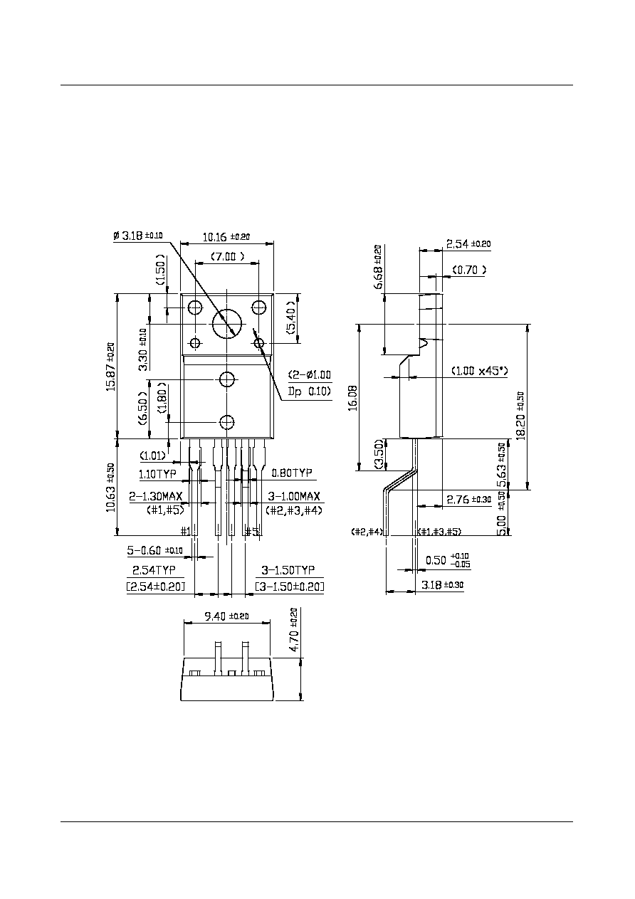
FSCQ-SERIES
42
Package Dimensions
Dimensions in Millimeters
TO-220F-5L(Forming)

FSCQ-SERIES
43
Package Dimensions
Dimensions in Millimeters
NOTES: UNLESS OTHERWISE SPECIFIED
A) THIS PACKAGE DOES NOT COMPLY
TO ANY CURRENT PACKAGING STANDARD.
B) ALL DIMENSIONS ARE IN MILLIMETERS.
C) DIMENSIONS ARE EXCLUSIVE OF BURRS,
MOLD FLASH, AND TIE BAR EXTRUSIONS.
15.70
15.30
24.70
24.30
2.54
4.50
0.90
0.70
MAX 1.00
MAX 2.00
36.50
35.50
23.20
22.80
1.70
1.30
0.80
0.50
3.48
2.88
3.55
3.15
10.20
9.80
4.70
4.30
12.00
11.00
1.50
4.30
3.70
2.80
2.20
2.55
2.15
3.65
3.05
3.06
2.46
9.70
9.30
6.05
5.65
5.30
4.70
2.10
1.70
(1.00)
R0.90
R0.90
R0.90
(1.65)
MKT-TO3PFC05revA
TO-3PF-7L(Forming)

FSCQ-SERIES
10/4/05 0.0m 001
©
2005 Fairchild Semiconductor Corporation
LIFE SUPPORT POLICY
FAIRCHILD'S PRODUCTS ARE NOT AUTHORIZED FOR USE AS CRITICAL COMPONENTS IN LIFE SUPPORT DEVICES
OR SYSTEMS WITHOUT THE EXPRESS WRITTEN APPROVAL OF THE PRESIDENT OF FAIRCHILD SEMICONDUCTOR
CORPORATION. As used herein:
1. Life support devices or systems are devices or systems
which, (a) are intended for surgical implant into the body,
or (b) support or sustain life, and (c) whose failure to
perform when properly used in accordance with
instructions for use provided in the labeling, can be
reasonably expected to result in a significant injury of the
user.
2. A critical component in any component of a life support
device or system whose failure to perform can be
reasonably expected to cause the failure of the life support
device or system, or to affect its safety or effectiveness.
www.fairchildsemi.com
DISCLAIMER
FAIRCHILD SEMICONDUCTOR RESERVES THE RIGHT TO MAKE CHANGES WITHOUT FURTHER NOTICE TO ANY
PRODUCTS HEREIN TO IMPROVE RELIABILITY, FUNCTION OR DESIGN. FAIRCHILD DOES NOT ASSUME ANY
LIABILITY ARISING OUT OF THE APPLICATION OR USE OF ANY PRODUCT OR CIRCUIT DESCRIBED HEREIN; NEITHER
DOES IT CONVEY ANY LICENSE UNDER ITS PATENT RIGHTS, NOR THE RIGHTS OF OTHERS.
Ordering Information
YDTU : Forming Type
SYDTU : Forming Type
Product Number
Package
Marking Code
BVdss
R
ds(ON)
Max.
FSCQ0565RTYDTU
TO-220F-5L(Forming)
CQ0565RT
650V
2.2
FSCQ0765RTYDTU
TO-220F-5L(Forming)
CQ0765RT
650V
1.6
FSCQ0965RTYDTU
TO-220F-5L(Forming)
CQ0965RT
650V
1.2
FSCQ1265RTYDTU
TO-220F-5L(Forming)
CQ1265RT
650V
0.9
FSCQ1465RTYDTU
TO-220F-5L(Forming)
CQ1465RT
650V
0.8
FSCQ1565RTYDTU
TO-220F-5L(Forming)
CQ1565RT
650V
0.7
FSCQ1565RPSYDTU
TO-3PF-7L(Forming)
CQ1565RP
650V
0.7