© 2005 Fairchild Semiconductor Corporation
DS500899
www.fairchildsemi.com
January 2005
Revised February 2005
FSUSB22 Low
V
o
l
t
age U
l
tr
a
L
o
w
Power USB
High
S
peed
(
480 Mbp
s
)
Dual
DPDT Swit
ch
FSUSB22
Low Voltage Ultra Low Power
USB High Speed (480 Mbps) Dual DPDT Switch
General Description
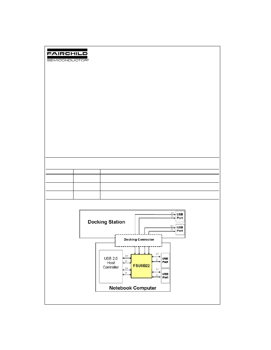
FSUSB22 is a low power high bandwidth analog switch
specially designed for applications of the switching of high
speed USB 2.0 signals in handset and consumer applica-
tions such as cell phone, digital camera, and notebook with
hubs or controllers of limited USB I/O. The wide bandwidth
(750MHz) of this switch allows signals to pass with mini-
mum edge and phase distortion. Superior channel-to-chan-
nel crosstalk results in minimal interference. It is
compatible with high speed USB2.0 standard.
Features
s
40dB OFF Isolation at 250MHz
s
40dB non-adjacent channel crosstalk at 250MHz
s
4.5
:
typical On Resistance (R
ON
)
s
3dB bandwidth: 750MHz
s
Low power consumption (1uA max)
s
Control input: TTL compatible
s
Bidirectional operation
s
USB high speed and full speed signaling capability
Applications
∑ Cell phone, PDA, digital camera, and notebook
Ordering Code:
Devices also available in Tape and Reel. Specify by appending suffix letter "X" to the ordering code.
Pb-Free package per JEDEC J-STD-020B.
Order Number
Package Number
Package Description
FSUSB22BQX
MLP016E
Pb-Free 16-Terminal Depopulated Quad Very-Thin Flat Pack No Leads (DQFN),
JEDEC MO-241, 2.5 x 3.5mm
FSUSB22QSC
(Preliminary)
MQA16
16-Lead Quarter Size Outline Package (QSOP), JEDEC MO-137, 0.150" Wide
FSUSB22MTC
(Preliminary)
MTC16
16-Lead Thin Shrink Small Outline Package (TSSOP), JEDEC MO-153, 4.4mm Wide

www.fairchildsemi.com
2
FSUS
B22
Analog Symbol
Pin Descriptions
Truth Table
Connection Diagrams
Pin Assignments for QSOP and TSSOP
(Preliminary)
Pad Assignments for DQFN
Pin Name
Description
OE
Bus Switch Enable
S
Select Input
A
Bus A
B
1
≠B
2
Bus B
S
OE
Function
X
H
Disconnect
L
L
A
B
1
H
L
A
B
2
3
www.fairchildsemi.com
FSUSB22
Absolute Maximum Ratings
(Note 1)
Recommended Operating
Conditions
(Note 3)
Note 1: The Absolute Maximum Ratings are those values beyond which
the safety of the device cannot be guaranteed. The device should not be
operated at these limits. The parametric values defined in the Electrical
Characteristics tables are not guaranteed at the absolute maximum rating.
The Recommended Operating Conditions tables will define the conditions
for actual device operation.
Note 2: The input and output negative voltage ratings may be exceeded if
the input and output diode current ratings are observed.
Note 3: Unused control inputs must be held HIGH or LOW. They may not
float.
DC Electrical Characteristics
Note 4: Typical values are at V
CC
3.0V and T
A
25
q
C
Note 5: Measured by the voltage drop between A and B pins at the indicated current through the switch. On Resistance is determined by the lower of the
voltages on the two (A or B) pins.
Note 6: Flatness is defined as the difference between the maximum and minimum value On Resistance over the specified range of conditions.
Supply Voltage (V
CC
)
0.5V to
4.6V
DC Switch Voltage (V
S
)
0.5V to V
CC
0.05V
DC Input Voltage (V
IN
) (Note 2)
0.5V to
4.6V
DC Input Diode Current (l
IK
) V
IN
0V
50 mA
DC Output (I
OUT
) Sink Current
128 mA
DC V
CC
/GND Current (I
CC
/I
GND
)
r
100 mA
Storage Temperature Range (T
STG
)
65
q
C to
150
q
C
ESD
Human Body Model
4kV
Power Supply Operating (V
CC
)
3.0V to 3.6V
Input Voltage (V
IN
)
0V to V
CC
Output Voltage (V
OUT
)
0V to V
CC
Input Rise and Fall Time (t
r
, t
f
)
Switch Control Input
0 ns/V to 5 ns/V
Switch I/O
0 ns/V to DC
Free Air Operating Temperature (T
A
)
40
q
C to
85
q
C
Symbol
Parameter
V
CC
(V)
T
A
40
q
C to
85
q
C
Units
Conditions
Min
Typ
(Note 4)
Max
V
IK
Clamp Diode Voltage
3.0
1.2
V
I
IN
18 mA
V
IH
HIGH Level Input Voltage
3.0 - 3.6
2.0
V
V
IL
LOW Level Input Voltage
3.0 - 3.6
0.8
V
I
I
Input Leakage Current
3.6
r
1.0
P
A
0
d
V
IN
d
3.6V
I
OFF
OFF-STATE Leakage Current
3.6
r
1.0
P
A
0
d
A, B
d
V
CC
R
ON
Switch On Resistance
3.0
5.0
7.0
:
V
IN
0.8V
(Note 5)
I
ON
8 mA
3.0
4.5
6.5
:
V
IN
3.0V
I
ON
8 mA
'
R
ON
Delta R
ON
3.0
0.3
:
V
IN
0.8V, V
IN
0V - 1.5V, I
ON
8 mA
R
FLAT(ON)
On Resistance Flatness (Note 6)
3.0
1.0
1.3
:
I
OUT
8 mA
I
CC
Quiescent Supply Current
3.6
1.0
P
A
V
IN
V
CC
or GND, I
OUT
0

www.fairchildsemi.com
4
FSUS
B22
AC Electrical Characteristics
Note 7: Typical values are at V
CC
3.3V and T
A
25
q
C
USB Related AC Electrical Characteristics
(Note 8)
Note 8: Typical values are at V
CC
3.3V and T
A
25
q
C
Capacitance
(Note 9)
Note 9: Typical values are at V
CC
3.3V and T
A
25
q
C
FIGURE 1. Gain vs. Frequency
Symbol
Parameter
V
CC
(V)
T
A
40
q
C to
85
q
C
Units
Conditions
Figure
Number
Min
Typ
(Note 7)
Max
t
ON
Turn ON Time S-to-Bus B
3.0 to 3.6
4.5
6.0
ns
Figures
5, 6
t
OFF
Turn OFF Time S-to-Bus B
3.0 to 3.6
2.5
4.0
ns
Figures
5, 6
t
PD
Propagation Delay
3.0 to 3.6
0.25
ns
C
L
10 pF
Figure
10
O
IRR
Non-Adjacent OFF-Isolation
3.0 to 3.6
55.0
dB
f
10MHz, R
L
50
:
Figure 7
X
TALK
Non-Adjacent Channel Crosstalk
3.0 to 3.6
75.0
dB
R
L
50
:
, f
10MHz
Figure 8
BW
3dB Bandwidth
3.0 to 3.6
750
MHz
R
L
50
:
Figure 9
Symbol
Parameter
V
CC
T
A
40
q
C to
85
q
C
Units
Conditions
Figure
(V)
Min
Typ
Max
Number
t
SK(O)
Channel-to-Channel Skew
3.0 to 3.6
0.051
ns
C
L
10 pF
Figures
10, 11
t
SK(P)
Skew of Opposite Transition
3.0 to 3.6
0.020
ns
C
L
10 pF
Figures
10, 11
of the Same Output
T
J
Total Jitter
3.0 to 3.6
0.210
ns
R
L
50
:
, C
L
10 pF
t
R
t
F
750ps at 480 Mbps
Symbol
Parameter
T
A
40
q
C to
85
q
C
Units
Conditions
Typ
C
IN
Control Pin Input Capacitance
2.5
pF
V
CC
0V
C
ON
A/B ON Capacitance
12.0
pF
V
CC
3.3V, OE
0V
C
OFF
Port B OFF Capacitance
4.5
pF
V
CC
and OE
3.3V

5
www.fairchildsemi.com
FSUSB22
FIGURE 2. OFF Isolation
FIGURE 3. Crosstalk
FIGURE 4. R
ON