 | –≠–ª–µ–∫—Ç—Ä–æ–Ω–Ω—ã–π –∫–æ–º–ø–æ–Ω–µ–Ω—Ç: H11C3 | –°–∫–∞—á–∞—Ç—å:  PDF PDF  ZIP ZIP |
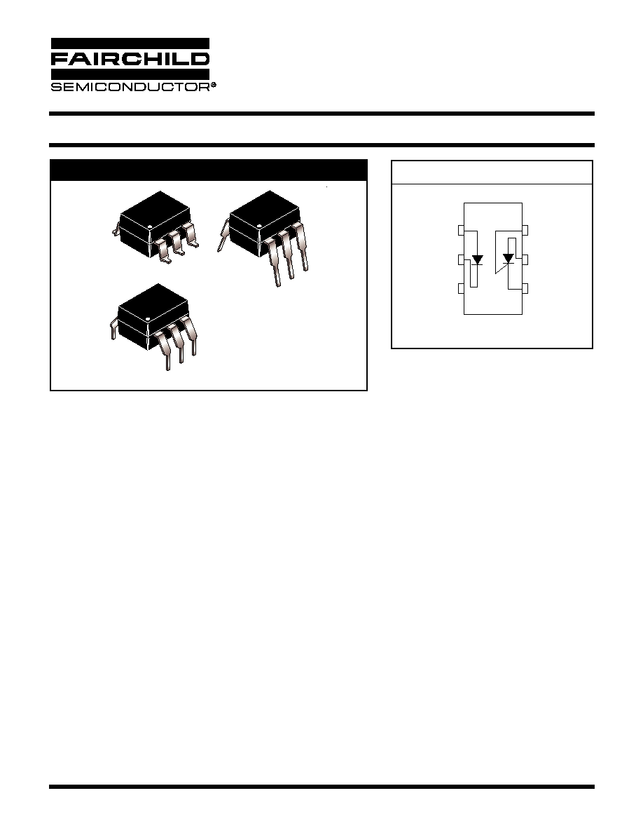
PACKAGE
SCHEMATIC
PHOTO SCR OPTOCOUPLERS
3/19/03
Page 1 of 11
© 2003 Fairchild Semiconductor Corporation
H11C1
H11C2
H11C3
H11C4
H11C5
H11C6
DESCRIPTION
The H11C series consists of a gallium-arsenide infrared emitting diode optically coupled with a light activated silicon controlled
rectifier in a dual-in-line package
FEATURES
∑
High efficiency, low degradation, liquid epitaxial LED
∑
Underwriters Laboratory (UL) recognized fl File #E90700
∑
VDE recognized (File #94766) ≠ ordering option .300. (e.g., H11C1.300)
∑
200V/400V Peak blocking voltage
∑
High isolation voltage - 5300V AC (RMS)
APPLICATIONS
∑
Low power logic circuits
∑
Telecommunications equipment
∑
Portable electronics
∑
Solid state relays
∑
Interfacing coupling systems of different potentials and impedances.
∑
10 A, T
2
L compatible, solid state relay
∑
25 W logic indicator lamp driver
∑
200 V symmetrical transistor coupler (H11C1, H11C2, H11C3)
∑
400 V symmetrical transistor coupler (H11C4, H11C5, H11C6)
6
1
6
1
6
1
CATHODE
ANODE
1
2
3
ANODE
CATHODE
4
5
6 GATE
N/C
3/19/03
Page 2 of 11
© 2003 Fairchild Semiconductor Corporation
PHOTO SCR OPTOCOUPLERS
H11C1
H11C2
H11C3
H11C4
H11C5
H11C6
Parameter
Symbol
Device
Value
Units
TOTAL DEVICE
Storage Temperature
T
STG
All
-55 to +150
∞C
Operating Temperature
T
OPR
All
-55 to +100
∞C
Lead Solder Temperature
T
SOL
All
260 for 10 sec
∞C
EMITTER
Continuous Forward Current
I
F
All
60
mA
Reverse Voltage
V
R
All
6
V
Forward Current - Peak (1 µs pulse, 300 pps)
I
F(pk)
All
3.0
A
LED Power Dissipation
P
D
All
100
mW
Derate above 25∞C
1.33
mW/∞C
DETECTOR
Power Dissipation (ambient)
P
D
All
400
mW
Derate linearly above 25∞C ambient
5.3
mW/∞C
Power Dissipation (case)
P
D
All
1
W
Derate linearly above 25∞C case
13.3
mW/∞C
Peak Reverse Gate Voltage
V
GR
All
6
V
RMS On-State Current
I
DM (RMS)
All
300
mA
Peak On-State Current (100 µS, 1% duty cycle)
I
DM (Peak)
All
10
A
Surge Current (10ms)
I
DM (Surge)
All
5
A
Peak Forward Voltage
V
DM
H11C1, H11C2, H11C3
200
V
Peak Forward Voltage
V
DM
H11C4, H11C5, H11C6
400
V
3/19/03
Page 3 of 11
© 2003 Fairchild Semiconductor Corporation
PHOTO SCR OPTOCOUPLERS
H11C1
H11C2
H11C3
H11C4
H11C5
H11C6
*Typical values at T
A
= 25∞C
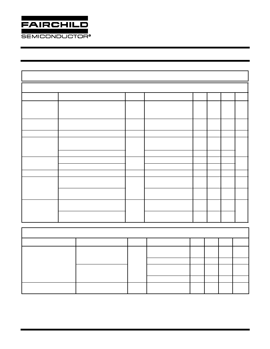
ELECTRICAL CHARACTERISTICS
(T
A
= 25∞C Unless otherwise specified.)
INDIVIDUAL COMPONENT CHARACTERISTICS
Parameter
Test Conditions
Symbol
Device
Min
Typ*
Max
Unit
EMITTER
Input Forward
Voltage
I
F
= 10 mA
V
F
All
1.2
1.5
V
Reverse Leakage
Current
V
R
= 3 V
I
R
All
10
µA
Capacitance
V
F
= 0 V, f = 1.0 MHz
C
J
All
50
pF
DETECTOR
Off-State Voltage
R
GK
= 10k
, T
A
= 100∞C, I
D
= 50µA
V
DM
H11C1, H11C2, H11C3
200
V
R
GK
= 10k
, T
A
= 100∞C, I
D
= 150µA
H11C4, H11C5, H11C6
400
Reverse Voltage
R
GK
= 10k
,T
A
= 100∞C, I
R
= 50µA
V
RM
H11C1, H11C2, H11C3
200
V
R
GK
= 10k
,T
A
= 100∞C, I
R
= 150µA
H11C4, H11C5, H11C6
400
On-State Voltage
I
TM
= 300 mA
V
TM
All
1.2
1.3
V
Off-State Current
V
DM
= 200V, T
A
= 100∞C, I
F
= 0 mA,
R
GK
= 10k
I
DM
H11C1, H11C2, H11C3
50
µA
V
DM
= 400V, T
A
= 100∞C, I
F
= 0 mA,
R
GK
= 10k
H11C4, H11C5, H11C6
150
Reverse Current
V
RM
= 200 V, T
A
= 100 ∞C, I
F
= 0 mA,
R
GK
= 10k
I
RM
H11C1, H11C2, H11C3
50
µA
V
RM
= 400 V, T
A
= 100 ∞C, I
F
= 0 mA,
R
GK
= 10k
H11C4, H11C5, H11C6
150
TRANSFER CHARACTERISTICS
(T
A
= 25∞C Unless otherwise specified.)
Characteristics
Test Conditions
Symbol
Device
Min
Typ*
Max
Units
Input Current to Trigger
V
AK
= 50 V, R
GK
= 10 k
I
FT
H11C1,H11C2,
H11C4, H11C5
20
H11C3, H11C6
30
mA
V
AK
= 100 V, R
GK
= 27 k
H11C1,H11C2,
H11C4, H11C5
11
H11C3, H11C6
14
Coupled dv/dt, input to
output (figure 8)
dv/dt
ALL
500
V/µS
3/19/03
Page 4 of 11
© 2003 Fairchild Semiconductor Corporation
PHOTO SCR OPTOCOUPLERS
H11C1
H11C2
H11C3
H11C4
H11C5
H11C6
*Typical values at T
A
= 25∞C
Note
1. For this test, LED pins 1 and 2 are common, and SCR pins 4, 5 and 6 are common.
ISOLATION CHARACTERISTICS
Characteristic
Test Conditions
Symbol
Min
Typ*
Max
Units
Isolation Voltage
(t = 1 min.) (note 1)
V
ISO
5300
V
Isolation Resistance
(note 1) (V
I-O
= 500 VDC)
R
ISO
10
11
Isolation Capacitance
(note 1) (f = 1 MHz, V
I-O
= 0)
C
I-O
0.8
pF
3/19/03
Page 5 of 11
© 2003 Fairchild Semiconductor Corporation
PHOTO SCR OPTOCOUPLERS
H11C1
H11C2
H11C3
H11C4
H11C5
H11C6
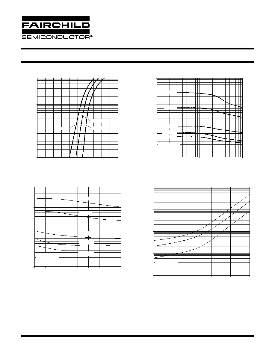
Figure 1. LED Forward Current vs. Forward Voltage
Figure 3. Input Trigger Current vs. Temperature
Figure 4. Off-State Current vs. Temperature
Figure 2. Trigger Current vs Anode-Cathode Voltage
FORWARD VOLTAGE - VF (V)
0.0
0.2
0.4
0.6
0.8
1.0
1.2
1.4
1.6
1.8
2.0
FOR
W
ARD CURRENT - IF (mA)
0.1
1
10
100
TA = 100∞C
TA = 25∞C
TA = -40∞C
V
AK
, ANODE-CATHODE VOLTAGE (V)
1
10
100
I
FT
, NORMAL
I
Z
ED TRIGGER
CURRENT
0.1
1
10
100
R
GK
= 300 ohm
R
GK
= 1K
R
GK
= 10K
NORMALIZED TO
V
AK
= 50V
R
GK
= 10K
T
A
= 25
o
C
R
GK
= 27K
R
GK
= 56K
T
A
, AMBIENT TEMPERATURE (
o
C)
-60
-40
-20
0
20
40
60
80
100
I
FT
, INPUT
TRIGGER CURRENT
, NORMALIZED
0.1
1
10
R
GK
= 300 ohm
R
GK
= 1K
R
GK
= 10K
R
GK
= 27K
R
GK
= 56K
NORMALIZED TO
T
A
= 25
o
C
R
GK
= 10K
V
AK
= 50V
T
A
, AMBIENT TEMPERATURE (
o
C)
0
20
40
60
80
100
I
DM
, OFF-
S
TAT
E FOR
W
ARD CURRE
NT
, NORMAL
IZED
0.1
1
10
100
1000
o
C
NORMALIZED TO
T
A
= 25
V
AK
= 50V
V
AK
= 400V
V
AK
= 200V
V
AK
= 50V
3/19/03
Page 6 of 11
© 2003 Fairchild Semiconductor Corporation
PHOTO SCR OPTOCOUPLERS
H11C1
H11C2
H11C3
H11C4
H11C5
H11C6
Figure 5. Forward Blocking Voltage, V
DM
vs. Temperature
T
A
, AMBIENT TEMPERATURE (
o
C)
0
20
40
60
80
100
V
DM
, FOR
W
ARD BLOCKING
V
O
L
T
A
GE (V)
300
350
400
450
500
550
600
650
700
R
GK
= 10K, 20K
R
GK
= 50K
R
GK
= 100K
ON-STATE VOLTAGE - VTM (V)
0.0
0.5
1.0
1.5
2.0
2.5
3.0
ON-ST
A
TE CURRENT - ITM (mA)
1
10
100
1000
Figure 6. On-State Characteristics
Figure 7. Holding Current, I
H
vs. Temperature
TA = 100
∞
C
TA = 25
∞
C
T
A
, AMBIENT TEMPERATURE (
o
C)
-60
-40
-20
0
20
40
60
80
100
I
H
, HOLDING CURRENT (
µ
A)
10
100
1000
10000
R
GK
= 300 ohm
R
GK
= 1K
R
GK
= 10K
R
GK
= 27K
R
GK
= 56K
3/19/03
Page 7 of 11
© 2003 Fairchild Semiconductor Corporation
PHOTO SCR OPTOCOUPLERS
H11C1
H11C2
H11C3
H11C4
H11C5
H11C6
TYPICAL APPLICATIONS
10A, T
2
L COMPATIBLE, SOLID
STATE RELAY
Use of the H11C4 for high sensitiv-
ity, 5300 V isolation capability,
provides this highly reliable solid
state relay design. This design is
compatible with 74, 74S and 74H
series T
2
L logic systems inputs
and 120V AC (H11C1, H11C2,
H11C3) or 220V AC (H11C4,
H11C5, H11C6) loads up to 10A.
25W, LOGIC INDICATOR LAMP DRIVER
The high surge capability and non-reactive input characteris-
tics of the H11C allow it to directly couple, without buffers,
T
2
L and DTL logic to indicator alarm devices, without danger
of introducing noise and logic glitches.
200V/400V SYMMETRICAL TRANSISTOR COUPLER
Use of the high voltage PNP portion of the H11C provides a 400V transistor capable of
conducting positive and negative signals with current transfer ratios of over 1%. This function
is useful in remote instrumentation, high voltage power supplies and test equipment. Care
should be taken not to exceed the H11C 400mW power dissipation rating when used at high
voltages.
+5V
470
"COIL"
H11CX
56K
100
47
47
SC146D
0.1
µF
LOAD
"CONTACT"
120 VAC (H11C1, H11C2, H11C3)
220 VAC (H11C4, H11C5, H11C6)
IN5060 (4)
120 VAC (H11C1, H11C2, H11C3)
220 VAC (H11C4, H11C5, H11C6)
LOGIC
+5V
56K
470
H11CX
0.1
µF
100
INPUT
INDICATOR
LAMP
OUTPUT
INPUT
H11CX
Fig. 8 Coupled dv/dt - Test Circuit
tp
+
H11C4
-
Vp
H
EXPONENTIAL
OSCILLOSCOPE
10 K
RAMP GEN.
100
+100 VAC
Vp = 800 Volts
tp = .010 Seconds
f = 25 Hertz
T
A
= 25
∞
C
dv / dt
.63 Vp
Vp
3/19/03
Page 8 of 11
© 2003 Fairchild Semiconductor Corporation
PHOTO SCR OPTOCOUPLERS
H11C1
H11C2
H11C3
H11C4
H11C5
H11C6
Package Dimensions (Through Hole)
Package Dimensions (Surface Mount)
Package Dimensions (0.4" Lead Spacing)
Recommended Pad Layout for
Surface Mount Leadform
0.100 (2.54)
TYP
0.020 (0.51)
MIN
0.350 (8.89)
0.330 (8.38)
0.270 (6.86)
0.240 (6.10)
PIN 1
ID.
0.022 (0.56)
0.016 (0.41)
0.070 (1.78)
0.045 (1.14)
0.200 (5.08)
0.115 (2.92)
0.300 (7.62)
TYP
0∞ to 15∞
0.154 (3.90)
0.100 (2.54)
SEATING PLANE
0.016 (0.40)
0.008 (0.20)
Lead Coplanarity : 0.004 (0.10) MAX
0.270 (6.86)
0.240 (6.10)
0.350 (8.89)
0.330 (8.38)
0.300 (7.62)
TYP
0.405 (10.30)
MAX
0.315 (8.00)
MIN
0.016 (0.40) MIN
2
5
PIN 1
ID.
0.016 (0.41)
0.008 (0.20)
0.100 (2.54)
TYP
0.022 (0.56)
0.016 (0.41)
0.070 (1.78)
0.045 (1.14)
0.200 (5.08)
0.165 (4.18)
4
3
0.020 (0.51)
MIN
1
6
SEATING PLANE
0.016 (0.40)
0.008 (0.20)
0.070 (1.78)
0.045 (1.14)
0.350 (8.89)
0.330 (8.38)
0.154 (3.90)
0.100 (2.54)
0.200 (5.08)
0.135 (3.43)
0.004 (0.10)
MIN
0.270 (6.86)
0.240 (6.10)
0.400 (10.16)
TYP
0∞ to 15∞
0.022 (0.56)
0.016 (0.41)
0.100 (2.54) TYP
0.070 (1.78)
0.060 (1.52)
0.030 (0.76)
0.100 (2.54)
0.295 (7.49)
0.415 (10.54)
Note
All dimensions are in inches (millimeters)
3/19/03
Page 9 of 11
© 2003 Fairchild Semiconductor Corporation
PHOTO SCR OPTOCOUPLERS
H11C1
H11C2
H11C3
H11C4
H11C5
H11C6
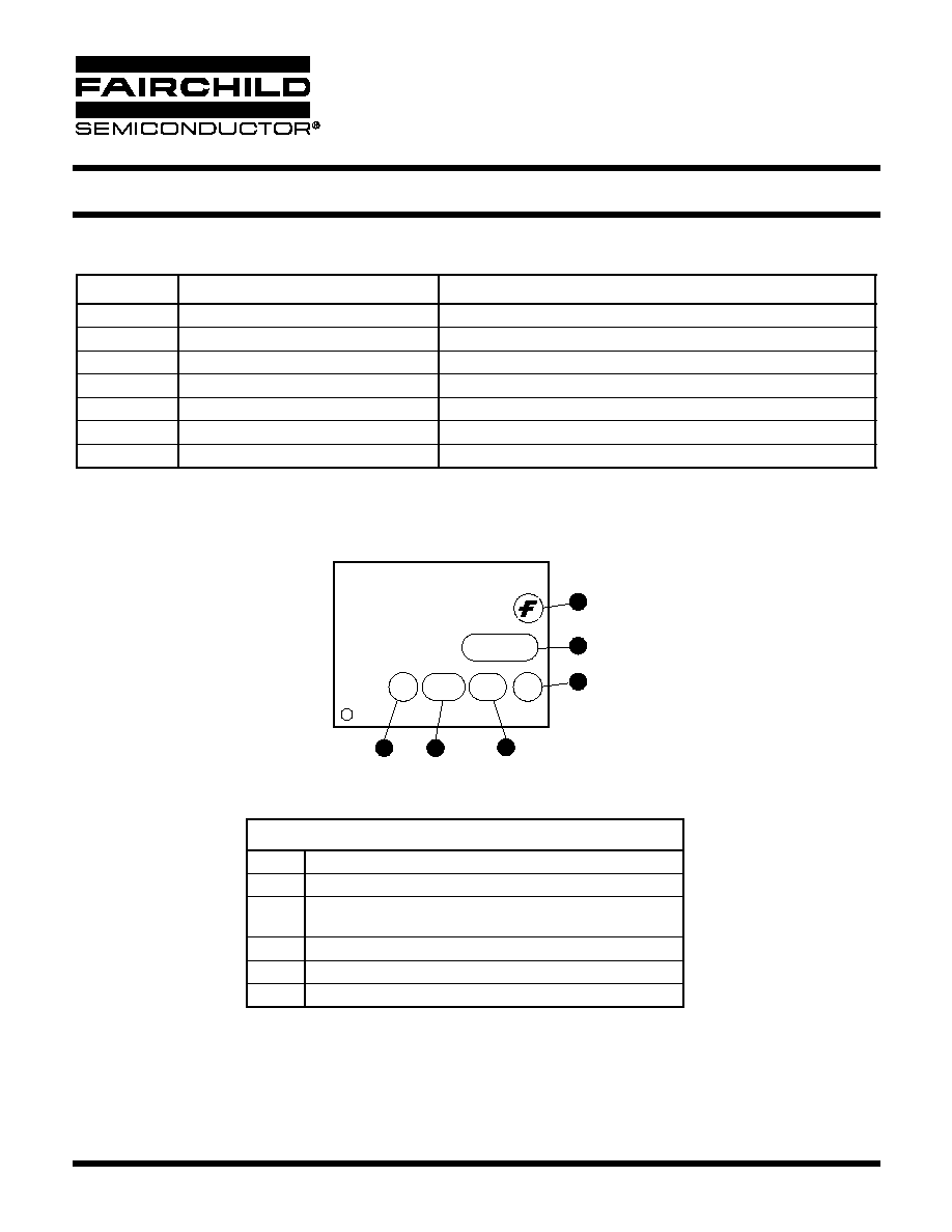
ORDERING INFORMATION
MARKING INFORMATION
Option
Order Entry Identifier
Description
S
.S
Surface Mount Lead Bend
SD
.SD
Surface Mount; Tape and Reel
W
.W
0.4" Lead Spacing
300
.300
VDE 0884
300W
.300W
VDE 0884, 0.4" Lead Spacing
3S
.3S
VDE 0884, Surface Mount
3SD
.3SD
VDE 0884, Surface Mount, Tape and Reel
H11C1
V XX YY K
1
2
6
4
3
5
Definitions
1
Fairchild logo
2
Device number
3
VDE mark (Note: Only appears on parts ordered with VDE
option ≠ See order entry table)
4
Two digit year code, e.g., `03'
5
Two digit work week ranging from `01' to `53'
6
Assembly package code
3/19/03
Page 10 of 11
© 2003 Fairchild Semiconductor Corporation
PHOTO SCR OPTOCOUPLERS
H11C1
H11C2
H11C3
H11C4
H11C5
H11C6
NOTE
All dimensions are in inches (millimeters)
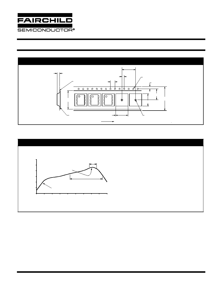
Reflow Profile (Black Package, No Suffix)
Carrier Tape Specifications
4.0
± 0.1
ÿ1.55
± 0.05
User Direction of Feed
4.0
± 0.1
1.75
± 0.10
7.5
± 0.1
16.0
± 0.3
12.0
± 0.1
0.30
± 0.05
13.2
± 0.2
4.85
± 0.20
0.1 MAX
10.30
± 0.20
9.55
± 0.20
ÿ1.6
± 0.1
∑ Peak reflow temperature: 225
∞
C (package surface temperature)
∑ Time of temperature higher than 183
∞
C for 60≠150 seconds
∑ One time soldering reflow is recommended
215
∞C, 10≠30 s
225
C peak
Time (Minute)
0
300
250
200
150
100
50
0
0.5
1
1.5
2
2.5
3
3.5
4
4.5
Te
mper
a
tur
e (
∞
C)
Time above 183
∞
C, 60≠150 sec
Ramp up = 3
C/sec

LIFE SUPPORT POLICY
FAIRCHILD'S PRODUCTS ARE NOT AUTHORIZED FOR USE AS CRITICAL COMPONENTS IN LIFE SUPPORT DEVICES
OR SYSTEMS WITHOUT THE EXPRESS WRITTEN APPROVAL OF THE PRESIDENT OF FAIRCHILD SEMICONDUCTOR
CORPORATION. As used herein:
1. Life support devices or systems are devices or systems
which, (a) are intended for surgical implant into the body, or
(b) support or sustain life, and (c) whose failure to perform
when properly used in accordance with instructions for use
provided in the labeling, can be reasonably expected to
result in a significant injury of the user.
2. A critical component in any component of a life support
device or system whose failure to perform can be
reasonably expected to cause the failure of the life support
device or system, or to affect its safety or effectiveness.
DISCLAIMER
FAIRCHILD SEMICONDUCTOR RESERVES THE RIGHT TO MAKE CHANGES WITHOUT FURTHER NOTICE TO
ANY PRODUCTS HEREIN TO IMPROVE RELIABILITY, FUNCTION OR DESIGN. FAIRCHILD DOES NOT ASSUME
ANY LIABILITY ARISING OUT OF THE APPLICATION OR USE OF ANY PRODUCT OR CIRCUIT DESCRIBED HEREIN;
NEITHER DOES IT CONVEY ANY LICENSE UNDER ITS PATENT RIGHTS, NOR THE RIGHTS OF OTHERS.
3/19/03
Page 11 of 11
© 2003 Fairchild Semiconductor Corporation
PHOTO SCR OPTOCOUPLERS
H11C1
H11C2
H11C3
H11C4
H11C5
H11C6