 | –≠–ª–µ–∫—Ç—Ä–æ–Ω–Ω—ã–π –∫–æ–º–ø–æ–Ω–µ–Ω—Ç: H11D4300 | –°–∫–∞—á–∞—Ç—å:  PDF PDF  ZIP ZIP |
Parameter
Symbol
Value
Units
TOTAL DEVICE
T
STG
-55 to +150
∞C
Storage Temperature
Operating Temperature
T
OPR
-55 to +100
∞C
Lead Solder Temperature
T
SOL
260 for 10 sec
∞C
Total Device Power Dissipation @ T
A
= 25∞C
P
D
260
mW
Derate above 25∞C
3.5
mW/∞C
EMITTER
I
F
80
mA
*Forward DC Current
*Reverse Input Voltage
V
R
6.0
V
*Forward Current - Peak (1µs pulse, 300pps)
I
F
(pk)
3.0
A
*LED Power Dissipation @ T
A
= 25∞C
P
D
150
mW
Derate above 25∞C
1.41
mW/∞C
FEATURES
∑ High Voltage
- H11D1, H11D2, BV
CER
= 300 V
- H11D3, H11D4, BV
CER
= 200 V
∑ High isolation voltage
- 5300 VAC RMS - 1 minute
- 7500 VAC PEAK - 1 minute
∑ Underwriters Laboratory (UL) recognized File# E90700
DESCRIPTION
The H11DX and 4N38 are phototransistor-type optically coupled optoisolators. An infrared emitting
diode manufactured from specially grown gallium arsenide is selectively coupled with a high voltage
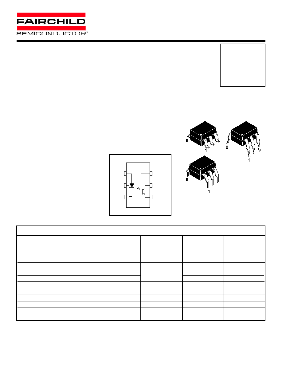
NPN silicon phototransistor. The device is supplied in a standard plastic six-pin dual-in-line package.
8/9/00 200046A
EMITTER
COLLECTOR
1
2
3
ANODE
CATHODE
4
5
6 BASE
N/C
HIGH VOLTAGE
PHOTOTRANSISTOR OPTOCOUPLERS
H11D1
H11D2
H11D3
H11D4
4N38
APPLICATIONS
∑ Power supply regulators
∑ Digital logic inputs
∑ Microprocessor inputs
∑ Appliance sensor systems
∑ Industrial controls
ABSOLUTE MAXIMUM RATINGS
8/9/00 200046A
H11D1, H11D2, H11D3, H11D4, 4N38
HIGH VOLTAGE
PHOTOTRANSISTOR OPTOCOUPLERS
Notes
* Parameters meet or exceed JEDEC registered data (for 4N38 only)
** All typical values at T
A
= 25∞C
ELECTRICAL CHARACTERISTICS
(T
A
= 25∞C Unless otherwise specified.)
Characteristic
Test Conditions
Symbol
Device
Min
Typ**
Max
Unit
EMITTER
(I
F
= 10 mA)
V
F
ALL
1.15
1.5
V
*Forward Voltage
Forward Voltage Temp.
!
V
F
ALL
-1.8
mV/∞C
Coefficient
!
T
A
Reverse Breakdown Voltage
(I
R
= 10 µA)
BV
R
ALL
6
25
V
Junction Capacitance
(V
F
= 0 V, f = 1 MHz)
C
J
ALL
50
pF
(V
F
= 1 V, f = 1 MHz)
ALL
65
pF
*Reverse Leakage Current
(V
R
= 6 V)
I
R
ALL
0.05
10
µA
DETECTOR
(R
BE
= 1 M
"
)
BV
CER
H11D1/2
300
*Breakdown Voltage
(I
C
= 1.0 mA, I
F
= 0)
H11D3/4
200
Collector to Emitter
(No R
BE
) (I
C
= 1.0 mA)
BV
CEO
4N38
80
H11D1/2
300
V
*Collector to Base
(I
C
= 100 µA, I
F
= 0)
BV
CBO
H11D3/4
200
4N38
80
Emitter to Base
(I
E
= 100 µA , I
F
= 0)
BV
EBO
4N38
7
Emitter to Collector
BV
ECO
ALL
7
10
(V
CE
= 200 V, I
F
= 0, T
A
= 25∞C)
H11D1/2
100
nA
*Leakage Current
(V
CE
= 200 V, I
F
= 0, T
A
= 100∞C)
I
CER
250
µA
Collector to Emitter
(V
CE
= 100 V, I
F
= 0, T
A
= 25∞C)
H11D3/4
100
nA
(R
BE
= 1 M
"
)
(V
CE
= 100 V, I
F
= 0, T
A
= 100∞C)
250
µA
(No R
BE
) (V
CE
= 60 V, I
F
= 0, T
A
= 25∞C)
I
CEO
4N38
50
nA
INDIVIDUAL COMPONENT CHARACTERISTICS
Parameter
Symbol
Value
Units
DETECTOR
300
mW
*Power Dissipation @ T
A
= 25∞C
P
D
Derate linearly above 25∞C
4.0
mW/∞C
H11D1 - H11D2
300
*Collector to Emitter Voltage
H11D3 - H11D4
V
CER
200
4N38
80
H11D1 - H11D2
300
V
*Collector Base Voltage
H11D3 - H11D4
V
CBO
200
4N38
80
*Emitter to Collector Voltage
H11D1 - H11D2
V
ECO
7
H11D3 - H11D4
Collector Current (Continuous)
100
mA
ABSOLUTE MAXIMUM RATINGS (Cont.)
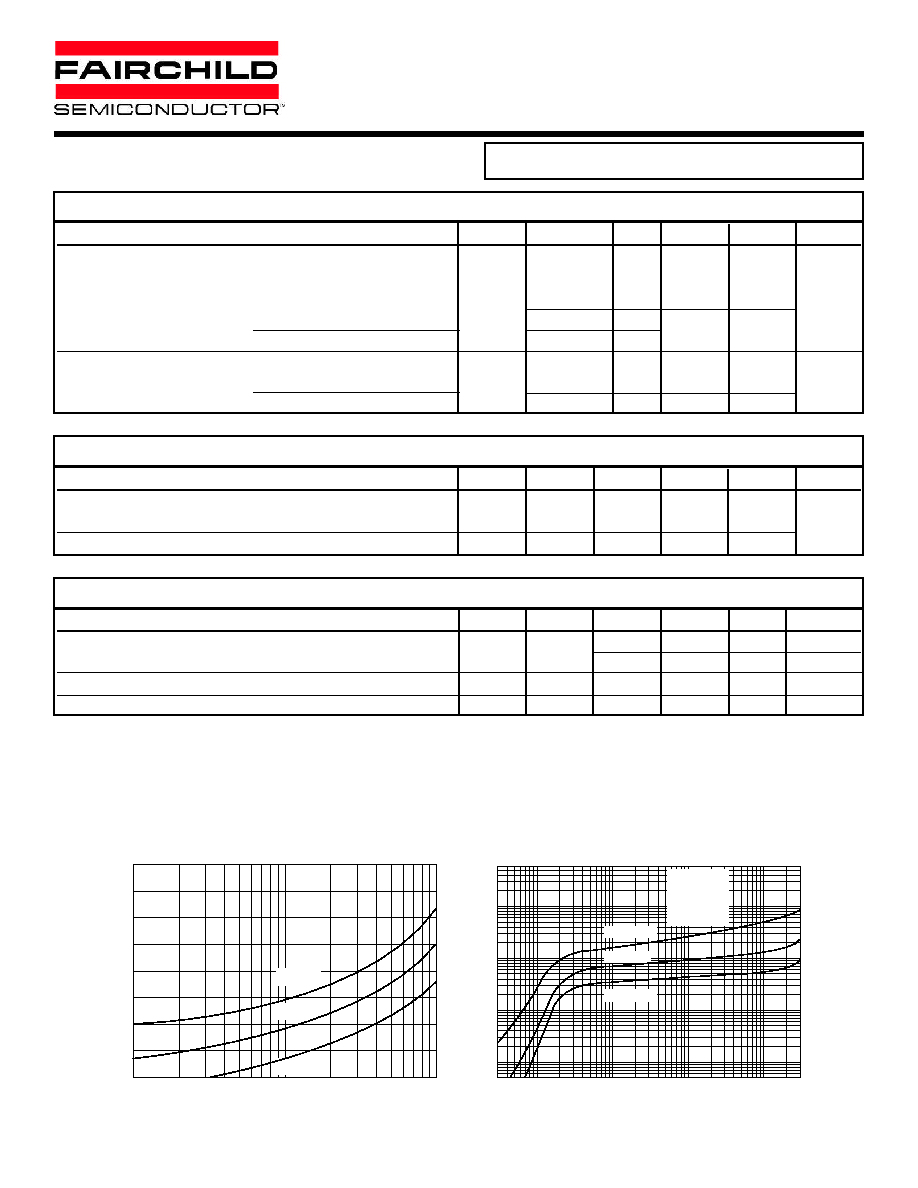
V
CE
- COLLECTOR VOLTAGE (V)
NORMALIZED I
CER
- OUTPUT CURRENT
Fig.2 Normalized Output Characteristics
0.1
1
10
100
0.01
0.1
1
10
Normalized to:
V
CE
= 10 V
I
F
= 10 mA
R
BE
= 10
6
T
A
= 25∞C
I
F
= 50 mA
I
F
= 5 mA
I
F
= 10 mA
I
F
- LED FORWARDCURRENT (mA)
V
F
- FOR
W
ARD
V
O
L
T
A
GE (V)
Fig.1 LED Forward Voltage vs. Forward Current
1
10
100
1.0
1.1
1.2
1.3
1.4
1.5
1.6
1.7
1.8
T
A
= 55∞C
T
A
= 25∞C
T
A
= 100∞C
8/9/00 200046A
H11D1, H11D2, H11D3, H11D4, 4N38
HIGH VOLTAGE
PHOTOTRANSISTOR OPTOCOUPLERS
DC Characteristic
Test Conditions
Symbol
Device
Min
Typ**
Max
Unit
EMITTER
H11D1
Current Transfer Ratio
(I
F
= 10 mA, V
CE
= 10 V)
H11D2
2 (20)
Collector to Emitter
(R
BE
= 1 M
"
)
CTR
H11D3
mA (%)
H11D4
1 (10)
(I
F
= 10 mA, V
CE
= 10 V)
4N38
2 (20)
(I
F
= 10 mA, I
C
= 0.5 mA)
H11D1/2/3/4
0.1
0.40
*Saturation Voltage
(R
BE
= 1 M
"
)
V
CE (SAT)
V
(I
F
= 20 mA, I
C
= 4 mA)
4N38
1.0
TRANSFER CHARACTERISTICS
Characteristic
Test Conditions
Symbol
Device
Min
Typ**
Max
Unit
SWITCHING TIMES
(V
CE
=10 V, I
CE
= 2 mA)
t
on
ALL
5
Non-Saturated Turn-on Time
µs
Turn-off Time
(R
L
= 100
"
) t
off
ALL
5
TRANSFER CHARACTERISTICS
Characteristic
Test Conditions
Symbol
Device
Min
Typ**
Max
Unit
Isolation Voltage
(I
I-O
#$
1 µA, 1 min.)
V
ISO
ALL
5300
(V
AC
RMS)
7500
(V
AC
PEAK)
Isolation Resistance
(V
I-O
= 500 VDC)
R
ISO
ALL
10
11
"
Isolation Capacitance
(f = 1 MHz)
C
ISO
ALL
0.5
pF
ISOLATION CHARACTERISTICS
Notes
* Parameters meet or exceed JEDEC registered data (for 4N38 only)
** All typical values at T
A
= 25∞C
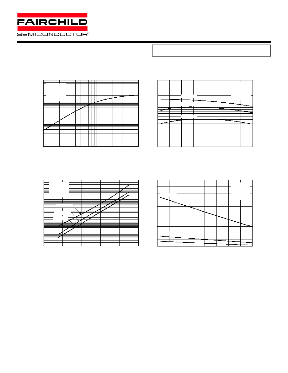
T
A
- AMBIENT TEMPERATURE (∞C)
NORMALIZED I
CER
- D
ARK CURRENT
Fig.3 Normalized Output Current vs. LED Input Current
I
F
- LED INPUT CURRENT (mA)
1
10
NORMALIZED I
CER
- OUTPUT CURRENT
0.01
0.1
1
10
Normalized to:
V
CE
= 10 V
I
F
= 10 mA
R
BE
= 10
6
T
A
= 25∞C
T
A
- AMBIENT TEMPERATURE (∞C)
NORMALIZED I
CER
- OUTPUT CURRENT
Fig.4 Normalized Output Current vs. Temperature
-60
-40
-20
0
20
40
60
80
100
0.1
1
Normalized to:
V
CE
= 10 V
I
F
= 10 mA
R
BE
= 10
6
T
A
= 25∞C
I
F
= 10 mA
I
F
= 5 mA
I
F
= 20 mA
T
A
- AMBIENT TEMPERATURE (∞C)
NORMALIZED I
CBO
- COLLECT
OR-BASE CURRENT
Normalized Collector-Base Current vs. Temperature
-60
-40
-20
0
20
40
60
80
100
0
1
2
3
4
5
6
7
8
9
10
Normalized to:
V
CE
= 10 V
I
F
= 10 mA
R
BE
= 10
6
T
A
= 25∞C
I
F
= 50 mA
I
F
= 10 mA
I
F
= 5 mA
Fig.5 Normalized Dark Current vs. Ambient Temperature
10
20
30
40
50
60
70
80
90
100
110
0.1
1
10
100
1000
10000
V
CE
= 300 V
V
CE
= 100 V
V
CE
= 50 V
Normalized to:
V
CE
= 100 V
R
BE
= 10
6
T
A
= 25∞C
8/9/00 200046A
H11D1, H11D2, H11D3, H11D4, 4N38
HIGH VOLTAGE
PHOTOTRANSISTOR OPTOCOUPLERS
Lead Coplanarity : 0.004 (0.10) MAX
0.270 (6.86)
0.240 (6.10)
0.350 (8.89)
0.330 (8.38)
0.300 (7.62)
TYP
0.405 (10.30)
MAX
0.315 (8.00)
MIN
0.016 (0.40) MIN
2
5
PIN 1
ID.
0.016 (0.41)
0.008 (0.20)
0.100 (2.54)
TYP
0.022 (0.56)
0.016 (0.41)
0.070 (1.78)
0.045 (1.14)
0.200 (5.08)
0.165 (4.18)
4
3
0.020 (0.51)
MIN
1
6
0.100 (2.54)
TYP
0.020 (0.51)
MIN
0.350 (8.89)
0.330 (8.38)
0.270 (6.86)
0.240 (6.10)
PIN 1
ID.
0.022 (0.56)
0.016 (0.41)
0.070 (1.78)
0.045 (1.14)
0.200 (5.08)
0.135 (3.43)
0.300 (7.62)
TYP
0∞ to 15∞
0.154 (3.90)
0.100 (2.54)
SEAT
I
N
G PLAN
E
0.016 (0.40)
0.008 (0.20)
3
2
1
4
5
6
SEATING
PL
ANE
0.016 (0.40)
0.008 (0.20)
0.070 (1.78)
0.045 (1.14)
0.350 (8.89)
0.330 (8.38)
0.154 (3.90)
0.100 (2.54)
0.200 (5.08)
0.135 (3.43)
0.004 (0.10)
MIN
0.270 (6.86)
0.240 (6.10)
0.400 (10.16)
TYP
0∞ to 15∞
0.022 (0.56)
0.016 (0.41)
0.100 (2.54) TYP
3
PIN 1
ID.
2
1
4
5
6
NOTE
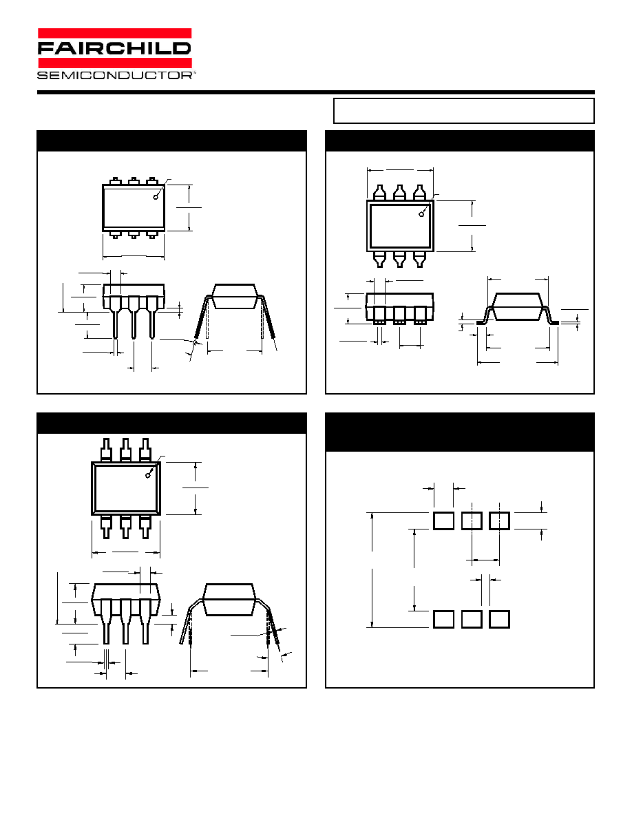
All dimensions are in inches (millimeters)
0.070 (1.78)
0.060 (1.52)
0.030 (0.76)
0.100 (2.54)
0.295 (7.49)
0.415 (10.54)
Package Dimensions (Surface Mount)
Package Dimensions (Through Hole)
Package Dimensions (0.4"Lead Spacing)
Recommended Pad Layout for
Surface Mount Leadform
8/9/00 200046A
H11D1, H11D2, H11D3, H11D4, 4N38
HIGH VOLTAGE
PHOTOTRANSISTOR OPTOCOUPLERS
S
.S
Surface Mount Lead Bend
SD
.SD
Surface Mount; Tape and reel
W
.W
0.4" Lead Spacing
300
.300
VDE 0884
300W
.300W
VDE 0884, 0.4" Lead Spacing
3S
.3S
VDE 0884, Surface Mount
3SD
.3SD
VDE 0884, Surface Mount, Tape & Reel
Option
Order Entry Identifier
Description
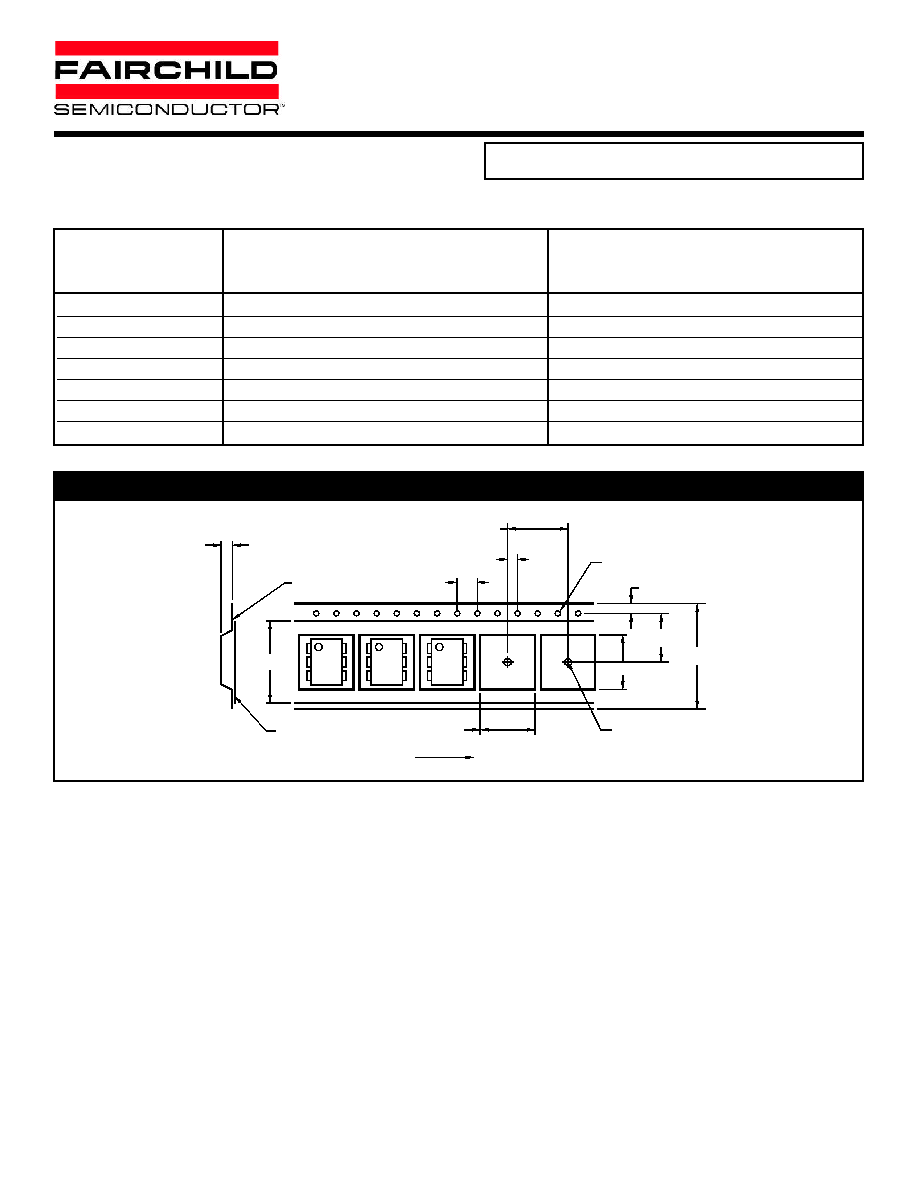
4.0 ± 0.1
ÿ1.55 ± 0.05
User Direction of Feed
4.0 ± 0.1
1.75 ± 0.10
7.5 ± 0.1
16.0 ± 0.3
12.0 ± 0.1
0.30 ± 0.05
13.2 ± 0.2
4.85 ± 0.20
0.1 MAX
10.30 ± 0.20
9.55 ± 0.20
ÿ1.6 ± 0.1
QT Carrier Tape Specifications ("D" Taping Orientation)
ORDERING INFORMATION
NOTE
All dimensions are in millimeters
8/9/00 200046A
H11D1, H11D2, H11D3, H11D4, 4N38
HIGH VOLTAGE
PHOTOTRANSISTOR OPTOCOUPLERS
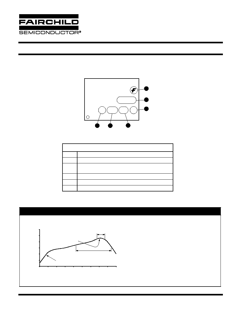
MARKING INFORMATION
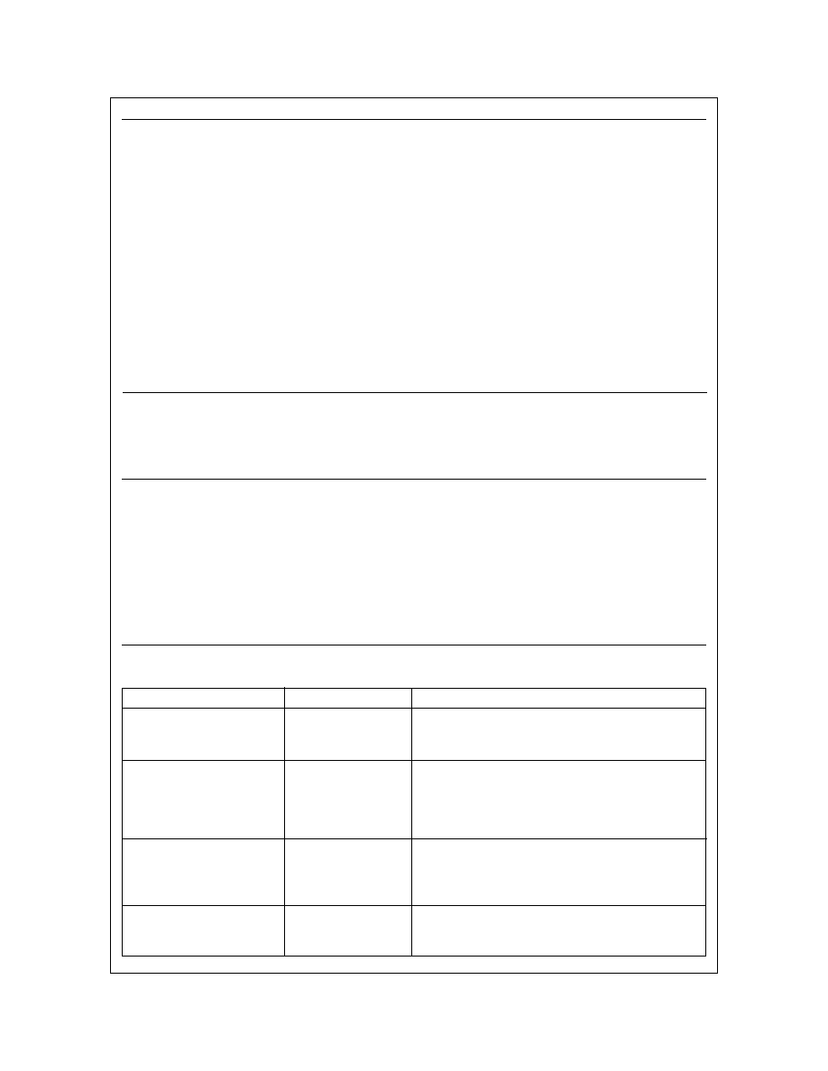
Reflow Profile (Black Package, No Suffix)
H11D1
V XX YY K
1
2
6
4
3
5
Definitions
1
Fairchild logo
2
Device number
3
VDE mark (Note: Only appears on parts ordered with VDE
option ≠ See order entry table)
4
Two digit year code, e.g., `03'
5
Two digit work week ranging from `01' to `53'
6
Assembly package code
∑ Peak reflow temperature: 225
∞
C (package surface temperature)
∑ Time of temperature higher than 183
∞
C for 60≠150 seconds
∑ One time soldering reflow is recommended
215
∞C, 10≠30 s
225
C peak
Time (Minute)
0
300
250
200
150
100
50
0
0.5
1
1.5
2
2.5
3
3.5
4
4.5
T
e
mper
a
tur
e (
∞
C)
Time above 183
∞
C, 60≠150 sec
Ramp up = 3
C/sec
DISCLAIMER
FAIRCHILD SEMICONDUCTOR RESERVES THE RIGHT TO MAKE CHANGES WITHOUT FURTHER NOTICE TO ANY
PRODUCTS HEREIN TO IMPROVE RELIABILITY, FUNCTION OR DESIGN. FAIRCHILD DOES NOT ASSUME ANY LIABILITY
ARISING OUT OF THE APPLICATION OR USE OF ANY PRODUCT OR CIRCUIT DESCRIBED HEREIN; NEITHER DOES IT
CONVEY ANY LICENSE UNDER ITS PATENT RIGHTS, NOR THE RIGHTS OF OTHERS.
TRADEMARKS
The following are registered and unregistered trademarks Fairchild Semiconductor owns or is authorized to use and is
not intended to be an exhaustive list of all such trademarks.
LIFE SUPPORT POLICY
FAIRCHILD'S PRODUCTS ARE NOT AUTHORIZED FOR USE AS CRITICAL COMPONENTS IN LIFE SUPPORT
DEVICES OR SYSTEMS WITHOUT THE EXPRESS WRITTEN APPROVAL OF FAIRCHILD SEMICONDUCTOR CORPORATION.
As used herein:
1. Life support devices or systems are devices or
systems which, (a) are intended for surgical implant into
the body, or (b) support or sustain life, or (c) whose
failure to perform when properly used in accordance
with instructions for use provided in the labeling, can be
reasonably expected to result in significant injury to the
user.
2. A critical component is any component of a life
support device or system whose failure to perform can
be reasonably expected to cause the failure of the life
support device or system, or to affect its safety or
effectiveness.
PRODUCT STATUS DEFINITIONS
Definition of Terms
Datasheet Identification
Product Status
Definition
Advance Information
Preliminary
No Identification Needed
Obsolete
This datasheet contains the design specifications for
product development. Specifications may change in
any manner without notice.
This datasheet contains preliminary data, and
supplementary data will be published at a later date.
Fairchild Semiconductor reserves the right to make
changes at any time without notice in order to improve
design.
This datasheet contains final specifications. Fairchild
Semiconductor reserves the right to make changes at
any time without notice in order to improve design.
This datasheet contains specifications on a product
that has been discontinued by Fairchild semiconductor.
The datasheet is printed for reference information only.
Formative or
In Design
First Production
Full Production
Not In Production
ISOPLANARTM
LittleFETTM
MICROCOUPLERTM
MicroFETTM
MicroPakTM
MICROWIRETM
MSXTM
MSXProTM
OCXTM
OCXProTM
OPTOLOGIC
OPTOPLANARTM
PACMANTM
POPTM
FAST
FASTrTM
FPSTM
FRFETTM
GlobalOptoisolatorTM
GTOTM
HiSeCTM
I
2
CTM
i-LoTM
ImpliedDisconnectTM
Rev. I13
ACExTM
ActiveArrayTM
BottomlessTM
CoolFETTM
CROSSVOLTTM
DOMETM
EcoSPARKTM
E
2
CMOSTM
EnSignaTM
FACTTM
FACT Quiet SeriesTM
Power247TM
PowerEdgeTM
PowerSaverTM
PowerTrench
QFET
QSTM
QT OptoelectronicsTM
Quiet SeriesTM
RapidConfigureTM
RapidConnectTM
µSerDesTM
SILENT SWITCHER
SMART STARTTM
SPMTM
StealthTM
SuperFETTM
SuperSOTTM-3
SuperSOTTM-6
SuperSOTTM-8
SyncFETTM
TinyLogic
TINYOPTOTM
TruTranslationTM
UHCTM
UltraFET
VCXTM
Across the board. Around the world.TM
The Power Franchise
Programmable Active DroopTM