 | –≠–ª–µ–∫—Ç—Ä–æ–Ω–Ω—ã–π –∫–æ–º–ø–æ–Ω–µ–Ω—Ç: H21LTI | –°–∫–∞—á–∞—Ç—å:  PDF PDF  ZIP ZIP |
+
E
+
D
2
0.129 (3.3)
0.119 (3.0)
0.433 (11.0)
0.422 (10.7)
0.315 (8.0)
0.295 (7.5)
0.272 (6.9)
0.055 (1.40)
0.045 (1.14)
0.110 (2.8)
0.091 (2.3)
0.055 (1.40)
0.045 (1.14)
1
3
5
4
0.020 (0.51) (SQ)
0.472 (12.0)
0.457 (11.6)
0.249 (6.35)
0.243 (6.15)
0.39 (1.00)
0.34 (0.85)
0.103 (2.60) NOM
0.125 (3.2)
0.119 (3.0)
ÿ 0.133 (3.4)
ÿ 0.126 (3.2)
(2X)
0.755 (19.2)
0.745 (18.9)
L
C
CL
L
C
Optical
CL
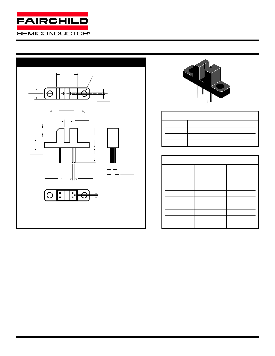
PIN 2 CATHODE
PIN 5 GND
PIN 4 V
PIN 3 V
CC
O
PIN 1 ANODE
PACKAGE DIMENSIONS
DESCRIPTION
The H21L series are slotted optical switches designed for multipurpose non contact sensing. They consist of a GaAs LED and a
silicon OPTOLOGICÆ. sensor packaged in an injection molded housing and facing each other across a .124" (3.15 mm) gap. The
output is either inverting or non-inverting, with a choice of totem-pole or open-collector configuration for TTL/CMOS compatibility
H21LTB
H21LTI
H21LOB
H21LOI
NOTES:
1. Dimensions for all drawings are in inches (mm).
2. Tolerance of ± .010 (.25) on all non-nominal dimensions
unless otherwise specified.
OPTOLOGICÆ OPTICAL
INTERRUPTER SWITCH
FEATURES
∑ Low cost
∑ Choice of inverter or buffer output functions
∑ 0.035" apertures
∑ Choice of open-collector or totem-pole output configuration
∑ Black plastic opaque housing
∑ TTL/CMOS compatible output functions
∑ Mounting tabs on housing
H21LTB
Totem-pole, buffer output
H21LTI
Totem-pole, inverter output
H21LOB
Open-collector, buffer output
H21LOI
Open-collector, inverter output
PART NUMBER DEFINITIONS
Part
LED
Output
Number
H21LTB
On
High
H21LTB
Off
Low
H21LTI
On
Low
H21LTI
Off
High
H21LOB
On
High
H21LOB Off
Low
H21LOI
On
Low
H21LOI Off
High
INPUT/OUTPUT TABLE
2001 Fairchild Semiconductor Corporation
DS300294
5/29/01
1 OF 8
www.fairchildsemi.com
www.fairchildsemi.com
2 OF 8
5/29/01
DS300294
H21LTB
H21LTI
H21LOB
H21LOI
OPTOLOGICÆ OPTICAL
INTERRUPTER SWITCH
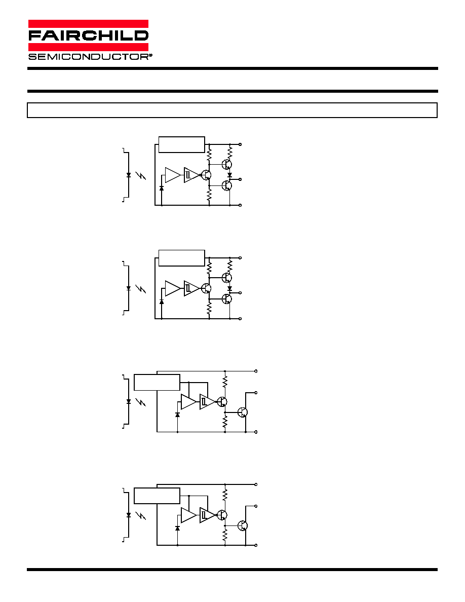
Open-Collector Output Buffer
H21LOB
CATHODE (2)
GND (5)
REGULATOR
VOLTAGE
V
CC
(3)
V
OUT
(4)
LA
ANODE (1)
ANODE (1)
CATHODE (2)
LA
REGULATOR
VOLTAGE
GND (5)
V
OUT
(4)
V
CC
(3)
ANODE (1)
CATHODE (2)
LA
REGULATOR
VOLTAGE
GND (5)
V
OUT
(4)
V
CC
(3)
ANODE (1)
CATHODE (2)
REGULATOR
VOLTAGE
LA
V
CC
(3)
V
OUT
(4)
GND (5)
Open-Collector Output Inverter
H21LOI
Totem-Pole Output inverter
H21LTI
Totem-Pole Output Buffer
H21LTB
SCHEMATICS

DS300294
5/29/01
3 OF 8
www.fairchildsemi.com
H21LTB
H21LTI
H21LOB
H21LOI
OPTOLOGICÆ OPTICAL
INTERRUPTER SWITCH
Parameter
Symbol
Rating
Units
Operating Temperature
T
OPR
-40 to +85
∞C
Storage Temperature
T
STG
-40 to +85
∞C
Soldering Temperature (Iron)
(3,4,5,6)
T
SOL-I
240 for 5 sec
∞C
Soldering Temperature (Flow)
(3,4,6)
T
SOL-F
260 for 10 sec
∞C
INPUT (EMITTER)
Continuous Forward Current
I
F
50
mA
Reverse Voltage
V
R
6
V
Power Dissipation
(1)
P
D
100
mW
OUTPUT (SENSOR)
Output Current
I
O
50
mA
Supply Voltage
V
CC
4.0 to 16
V
Output Voltage
V
O
30
V
Power Dissipation
(2)
P
D
150
mW
ABSOLUTE MAXIMUM RATINGS
(T
A
= 25∞C unless otherwise specified)
NOTES
(Applies to Max Ratings and Characteristics Tables.)
1. Derate power dissipation linearly 1.67 mW/∞C above 25∞C.
2. Derate power dissipation linearly 2.50 mW/∞C above 25∞C.
3. RMA flux is recommended.
4. Methanol or isopropyl alcohols are recommended as
cleaning agents.
5. Soldering iron
1/16"
(1.6mm) from housing.
6. As long as leads are not under any stress or spring tension.

www.fairchildsemi.com
4 OF 8
5/29/01
DS300294
H21LTB
H21LTI
H21LOB
H21LOI
OPTOLOGICÆ OPTICAL
INTERRUPTER SWITCH
PARAMETER
TEST CONDITIONS
SYMBOL
MIN.
TYP.
MAX.
UNITS
INPUT (EMITTER)
Forward Voltage
I
F
= 20 mA
V
F
--
1.5
V
Reverse Leakage Current
V
R
= 5 V
I
R
--
10
µA
OUTPUT (SENSOR)
Supply Current
V
CC
= 5 V
I
CC
--
5
mA
COUPLED
Low Level Output Voltage
I
F
= 0 mA, V
CC
= 5 V, R
L
= 100
V
OL
--
0.4
V
H21LTB, H21LOB
Low Level Output Voltage
I
F
= 15 mA, V
CC
= 5 V, R
L
= 360
V
OL
--
0.4
V
H21LTI, H21LOI
High Level Output Voltage
I
F
= 15 mA, V
CC
= 5 V, I
OH
= -800 µA
V
OH
2.4
--
V
H21LTB
High Level Output Voltage
I
F
= 0 mA, V
CC
= 5 V, I
OH
= -800 µA
V
OH
2.4
--
V
H21LTI
High Level Output Current
I
F
= 0 mA, V
CC
= 5 V, I
OH
= -800 µA
I
OH
100
µA
H21LOB
High Level Output Current
I
F
= 0 mA, V
CC
= 5 V, V
OH
= 30 V
I
OH
--
100
µA
H21LOI
Turn on Threshold Current
V
CC
= 5 V, R
L
= 360
I
F
(+)
--
15
mA
Turn off Threshold Current
V
CC
= 5 V, R
L
= 360
I
F
(-)
0.50
--
mA
Hysteresis Ratio
I
F
(+) / I
F
(-)
1.2
Propagation Delay
V
CC
= 5 V, R
L
= 360
(See Fig, 9)
t
PLH,
t
PHL
5
µs
Output Rise and Fall Time
V
CC
= 5 V, R
L
= 360
(See Fig, 9)
t
r,
t
f
70
ns
ELECTRICAL / OPTICAL CHARACTERISTICS
(T
A
=25∞C)
DS300294
5/29/01
5 OF 8
www.fairchildsemi.com
H21LTB
H21LTI
H21LOB
H21LOI
OPTOLOGICÆ OPTICAL
INTERRUPTER SWITCH
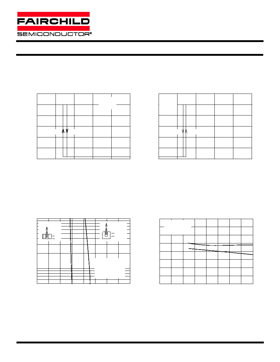
Fig. 4 Normalized Threshold Current vs. Supply Voltage
V
CC
- Supply Voltage (V)
0
2
4
6
8
10
12
14
16
I
F
- Nor
maliz
ed
Threshold Current
0.0
0.2
0.4
0.6
0.8
1.0
1.2
1.4
1.6
Normalized to:
Turn ON Threshold
V
CC
= 5 V
T
A
= 25∞C
I
F (ON)
I
F (OFF)
Fig. 1 Output Voltage vs. Input Current (Inverters)
I
F
- Input Current (mA)
I
F
- Input Current (mA)
0
1
2
3
4
5
V
O
- Output
V
o
ltage (V)
V
O
- Output
V
o
ltage (V)
0
1
2
3
4
5
6
V
OH
V
OL
V
CC
= 5 V
R
L
= 270
T
A
= 25∞C
I
F (ON)
I
F (OFF)
Fig. 3 Normalized Threshold Current vs. Shield Distance
d - Distance (mm)
0
1
2
3
4
5
6
7
8
I
F(ON)
- Nor
maliz
ed
Threshold Current
1
10
+
E
D
+
d
Black Shield
0
0
Black Shield
d
Normalized to:
V
CC
= 5 V
I
F
= 20 mA Pulsed
Pulse Width = 100 µs
Duty Cycle = 0.1%
Fig. 2 Output Voltage vs. Input Current (Buffers)
0
1
2
3
4
5
0
1
2
3
4
5
6
V
OL
V
OH
I
F (OFF)
I
F (ON)
V
CC
= 5 V
R
L
= 270
T
A
= 25∞C
www.fairchildsemi.com
6 OF 8
5/29/01
DS300294
H21LTB
H21LTI
H21LOB
H21LOI
OPTOLOGICÆ OPTICAL
INTERRUPTER SWITCH
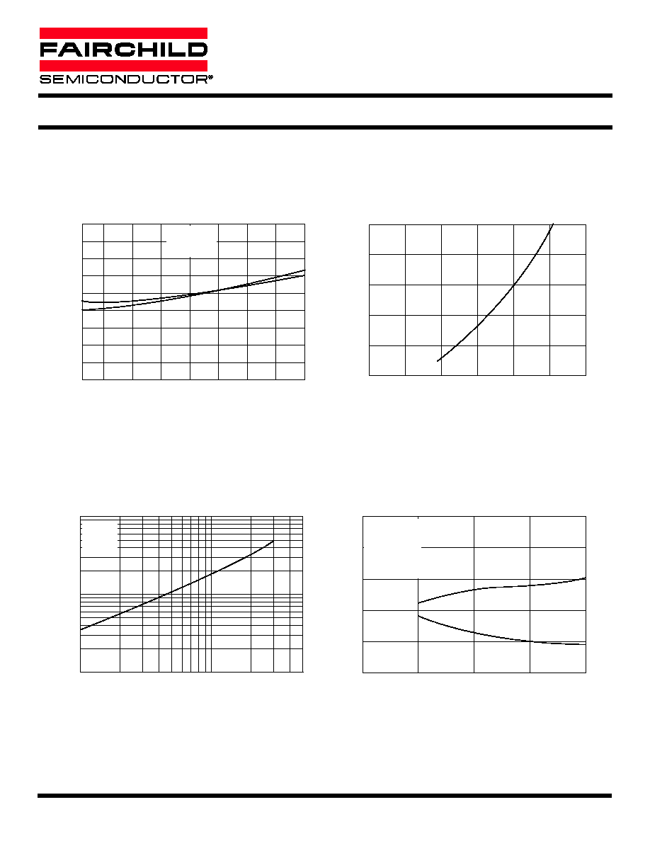
Fig. 7 Low Output Voltage vs. Output Current
I
O
- Output Current (mA)
1
10
V
OL
- Output
V
oltage
, Lo
w (V)
0.01
0.1
1
V
CC
= 5 V
T
A
= 25∞C
I
F
= 10 mA
Fig. 6 Forward Current vs. Forward Voltage
V
F
- Forward Voltage (V)
1.0
1.1
1.2
1.3
1.4
1.5
1.6
I
F
- F
o
rw
ard Current (mA)
0
20
40
60
80
100
Fig. 8 Response Time vs. Forward Current
I
F
- Forward Current (mA)
0
5
10
15
20
Response Dela
y
Time (us)
0
1
2
3
4
5
T
PHL
T
PLH
V
CC
= 5 V
R
L
= 270
T
A
= 25∞C
I
F
Pulsed
T = 10 ms
Duty Cycle = 50%
T
A
= 25∞C
Fig. 5 Normalized Threshold Current
vs. Ambient Temperature
T
A
- Ambient Temperature (
∞C)
-40
-20
0
20
40
60
80
100
I
F
- Nor
maliz
ed
Threshold Current
0.0
0.2
0.4
0.6
0.8
1.0
1.2
1.4
1.6
1.8
I
F (ON)
I
F (OFF)
I
F (OFF)
I
F (ON)
Normalized to:
V
CC
= 5 V
T
A
= 25∞C
DS300294
5/29/01
7 OF 8
www.fairchildsemi.com
H21LTB
H21LTI
H21LOB
H21LOI
OPTOLOGICÆ OPTICAL
INTERRUPTER SWITCH
C
2
R
2
R
1
1
C
.1 uf
bypass
5V
GND
Pulse
Generator
V = 5V
f = 10 KHz
d.c. = 50%
O
1
R = 360
R = 180
2
1
C = 15 pf
C = 20 pf
2
stray wire capacitance
C and C include probe and
1
2
Fig. 9 Switching Speed Test Circuit
PLH
r
t
PHL
t
50%
90%
10%
OH
V
OL
V
10%
90%
50%
Output
V
O
t
f
t
0 mA
OH
PHL
0 mA
t
V
PLH
50%
t
10%
90%
90%
10%
r
t
f
t
Output
O
V
OL
V
+
-
V
IN
R
IN
.1 uf
bypass
L
R
V
CC
GND
O
V
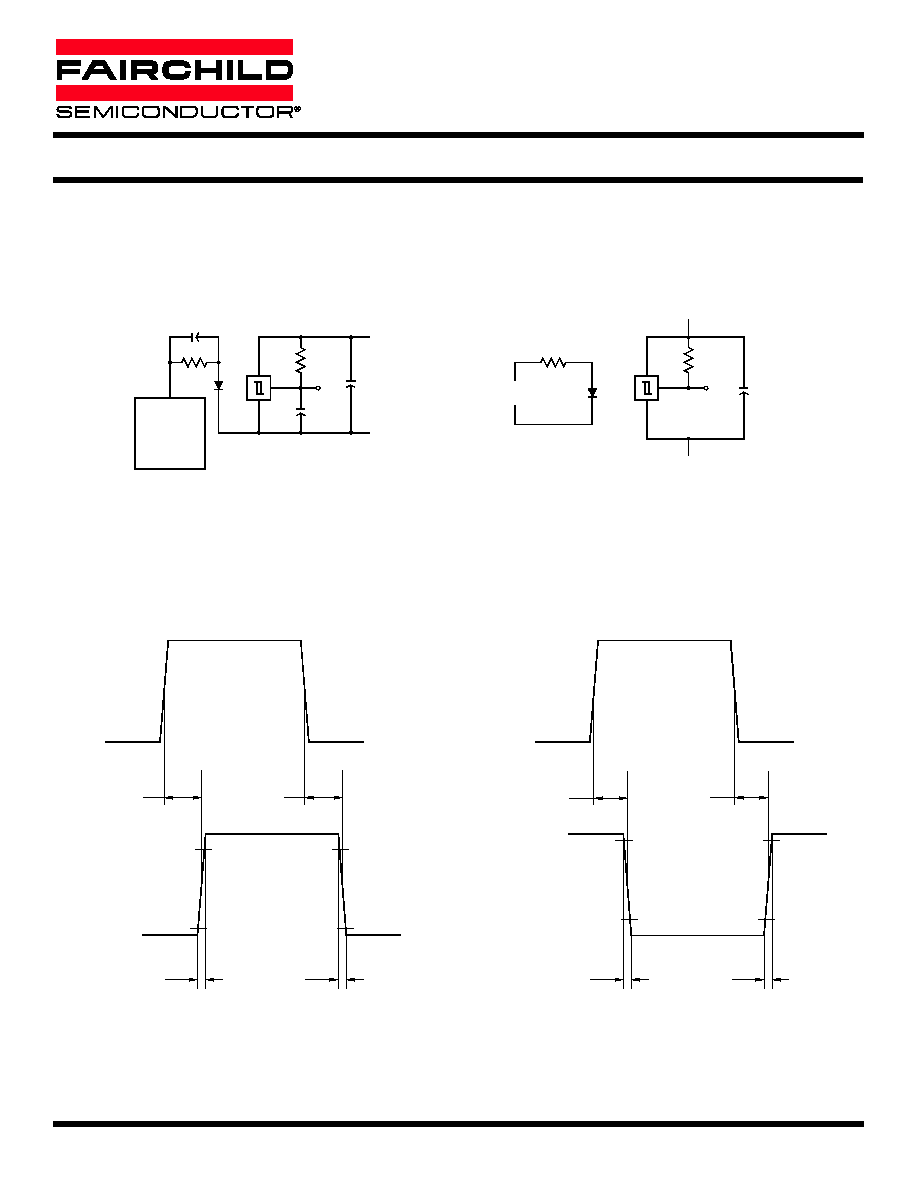
Fig. 10 Typical Operating Circuit
Fig. 11 Switching Times Definition for Buffers
Fig. 12 Switching Times Definition for Inverters

www.fairchildsemi.com
8 OF 8
5/29/01
DS300294
H21LTB
H21LTI
H21LOB
H21LOI
OPTOLOGICÆ OPTICAL
INTERRUPTER SWITCH
DISCLAIMER
FAIRCHILD SEMICONDUCTOR RESERVES THE RIGHT TO MAKE CHANGES WITHOUT FURTHER NOTICE TO
ANY PRODUCTS HEREIN TO IMPROVE RELIABILITY, FUNCTION OR DESIGN. FAIRCHILD DOES NOT ASSUME
ANY LIABILITY ARISING OUT OF THE APPLICATION OR USE OF ANY PRODUCT OR CIRCUIT DESCRIBED
HEREIN; NEITHER DOES IT CONVEY ANY LICENSE UNDER ITS PATENT RIGHTS, NOR THE RIGHTS OF
OTHERS.
LIFE SUPPORT POLICY
FAIRCHILD'S PRODUCTS ARE NOT AUTHORIZED FOR USE AS CRITICAL COMPONENTS IN LIFE SUPPORT
DEVICES OR SYSTEMS WITHOUT THE EXPRESS WRITTEN APPROVAL OF THE PRESIDENT OF FAIRCHILD
SEMICONDUCTOR CORPORATION. As used herein:
1. Life support devices or systems are devices or
systems which, (a) are intended for surgical
implant into the body,or (b) support or sustain life,
and (c) whose failure to perform when properly
used in accordance with instructions for use provided
in labeling, can be reasonably expected to result in a
significant injury of the user.
2. A critical component in any component of a life support
device or system whose failure to perform can be
reasonably expected to cause the failure of the life
support device or system, or to affect its safety or
effectiveness.